

VN220
/ VN220(011Y) / VN220(012Y)
HIGH SIDE SMART POWER SOLID STATE RELAY
TYPE V
VN220
VN220(011Y)
VN220(012Y)
■ OUTPUT CURRENT (CONTINUOUS): 28A AT
DSS
60V 0.05Ω 28A
TC=25°C
■ THERMAL SHUT-DOWN
■ UNDERVOLTAGE SHUT-DOWN
■ OPEN DRAIN DIAGNOSTIC OUTPUT
■ VERY LOW STAND-BY POWER DISSIPATION
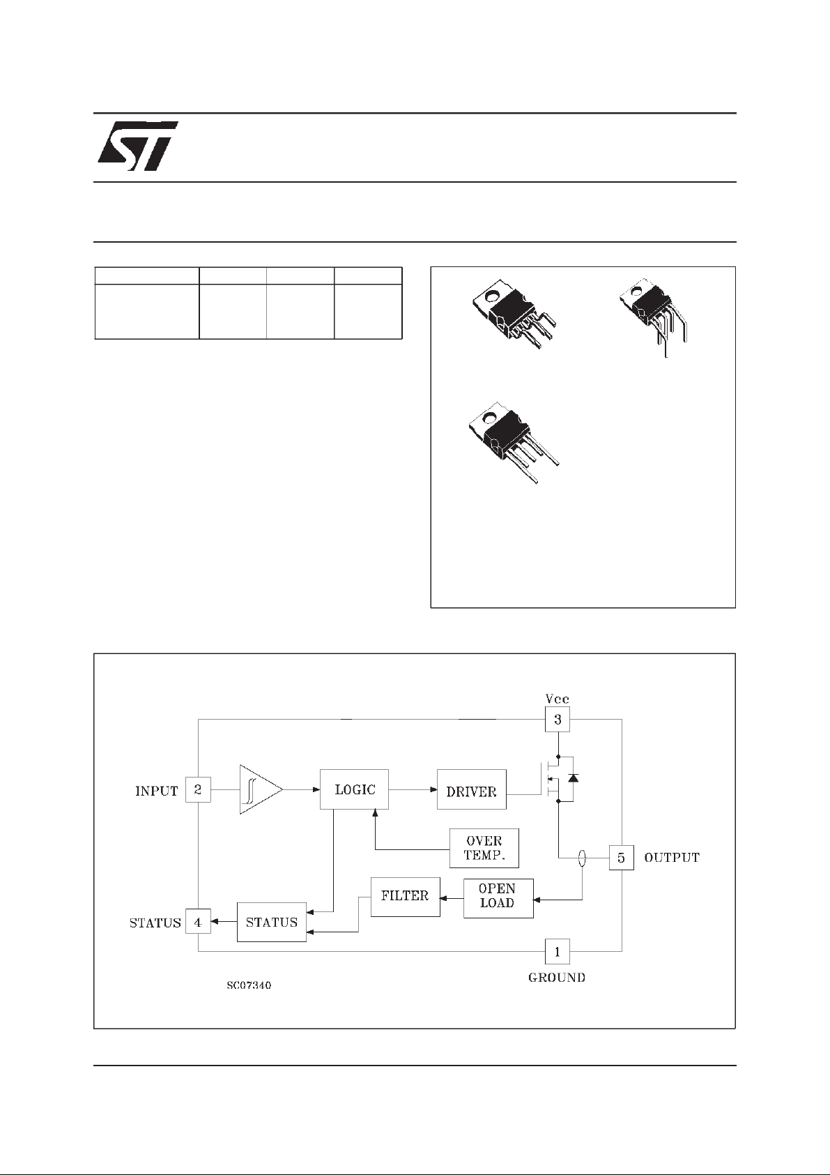
DESCRIPTION
The VN220 is a monolithic device designed in
STMicroelectronics VIPower technology,
intended for driving resistive or inductive loads
with one side grounded. Built-in thermal shutdown protects the chip from overtemperature and
short circuit. The open drain diagnostic output
indicates open circuit (no load) and
overtemperature status.
R
DS(on)
I
OUT
PENTAWATT PENTAWATT
(vertical) (horizontal)
PENTAWATT
(in-line)
ORDER CODES:
PENTAWATT vertical VN220
PENTAWATT horizontal VN220(011Y)
PENTAWATT in-line
VN220(012Y)
BLOCK DIAGRAM
September 1999 1/10
VN220 / VN220(011Y) / VN220(012Y)
ABSOLUTE MAXIMUM RATING
Symbol Parameter Value Unit
V
(BR)DSS
V
DS(off)
V
DS
I
OUT
I
R
I
IN
V
V
STAT
-V
CC
I
STAT
V
ESD
P
tot
T
T
stg
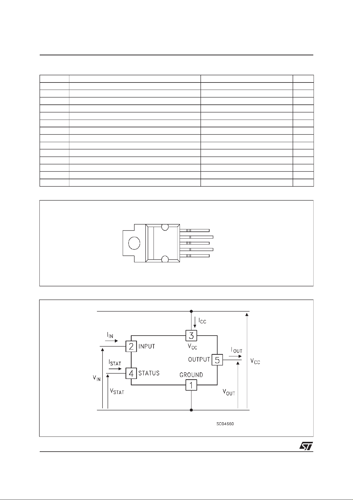
CONNECTION DIAGRAM (TOP VIEW)
Drain-Source Breakdown Voltage 60 V
Drain-Source Voltage (OFF STATE) 60 V
Drain-Source Voltage (Output Shorted to Ground) 30 V
Output Current (cont.) 28 A
Reverse Output Current -28 A
Input Current +/-10 mA
Input Voltage 35 V
IN
Status Output Voltage 35 V
Reverse Supply Voltage -4 V
Status Current +/-10 mA
Electrostatic Discharge (1.5KΩ; 100pF) 2000 V
Power Dissipation at Tc≤ 25°C60W
Junction Operating Temperature -40 to 150 °C
j
Storage temperature -55 to 150 °C
CURRENT AND VOLTAGE CONVENTIONS
5
4
3
2
1
OUTPUT
STATUS
V
CC
INPUT
GROUND
2/10
1

VN220 / VN220(011Y) / VN220(012Y)
THERMAL DATA
Symbol Parameter Value Unit
R
thj-case
R
thj-amb
Thermal resistance junction-case (MAX) 2.08 °C/W
Thermal resistance junction-ambient (MAX) 60 °C/W
ELECTRICAL CHARACTERISTICS (V
=13V; -40°C ≤ Tj≤ 125°C unless otherwise specified)
CC
POWER
Symbol Parameter Test Conditions Min Typ Max Unit
V
CC
R
I
S
SWITCHING
Symbol Parameter Test Conditions Min Typ Max Unit
t
d(on)
t
t
d(off)
t
LOGIC INPUT
Symbol Parameter Test Conditions Min Typ Max Unit
V
V
V
I(hyst)
I
IN
V
ICL
Supply Voltage 12 30 V
=3.5A
I
On State Resistance
on
OUT
=100mA; Tj=25°C
I
OUT
Off state
Supply Current
Turn-on Delay Time of
Output Current
Rise Time of Output
r
Current
Turn-off Delay Time of
Output Current
Fall Time of Output
f
Current
Input Low Level Voltage 1.5 V
IL
Input High Level Voltage 6 (*) V
IH
On State; Tj=25°C
On State; T
I
OUT
=100°C
j
=3.5A; Resistive Load;
Input Rise Time<0.1µs; T
=3.5A; Resistive Load;
I
OUT
Input Rise Time<0.1µs; T
=3.5A; Resistive Load;
I
OUT
Input Rise Time<0.1µs; T
=3.5A; Resistive Load;
I
OUT
Input Rise Time<0.1µs; T
=25°C
j
=25°C
j
=25°C
j
=25°C
j
20 µs
200 µs
30 µs
5 µs
Input Hysteresis Voltage 1 V
Input Current VIN=10V 600 µA
Input Clamp Voltage IIN=1mA 31 36 V
0.05
1.33
1
8
6
Ω
Ω
mA
mA
mA
PROTECTIONS AND DIAGNOSTIC
Symbol Parameter Test Conditions Min Typ Max Unit
V
STAT
I
STAT
I
OL
t
ol
T
TSD
T
V
STATCL
(*) The VIHis internally clamped at 6V about. It is possible to connect this pin to a higher voltage via an external resistor calculated to not
exceed 10mA at the input pin.
(•) Statusdetermination > 100
Status Output Voltage I
Status Output Leakage
Current
=5mA (Fault Condition) 0.9 2.5 V
STAT
=30V 100 µA
V
STAT
Open Load Current Level 3 9 20 mA
Open Load Filtering Time 1 10 ms
Thermal Shut-down
Temperature
Reset Temperature 125 °C
R
Diagnostic Input Clamp
(•)
Voltage
IIN=1mA 31 36 V
150 °C
µs after the switching edge.
3/10
1

VN220 / VN220(011Y) / VN220(012Y)
FUNCTIONAL DESCRIPTION
The VN220 provides protection against a short circuit on
the output and senses the output current to detect an
open load. When one of these two faults is detected the
diagnostic output is taken low.
OPEN LOAD DETECTION
When the device is first turned on, only the auxiliary
DMOS device is turned on. If the load current remains
below 9mA (typical), the open load signal is active and
the diagnostic output is low. When the load current goes
above 9 mA the open load detection becomes inactive
and the diagnostic goes high. When the load current
exceeds 300 mA, the main DMOS (50 mΩ) turns on.
When the load current drops below 240 mA, the main
DMOS is turned off but no open load signal is generated
and the auxiliary DMOS is still turned on. If the load
current drops below 9mA, again the open load signal is
generated and the diagnostic output goes low.
SHORT CIRCUIT PROTECTION
Short circuit protection is achieved using the fast
response of the thermal shut-down circuit. The only
current limitation in this condition is the saturation current
of the DMOS devices and the external wiring resistance.
Under this condition the device can survive a short circuit
up to 30V across DMOS devices.
THERMAL PROTECTION
The device is internally protected against over
temperature by the thermal protection circuit. When the
device junction temperature exceeds the protection limit,
the output is latched off. To turn on the output again, the
input signal must be taken low to reset the latch, then
high again to turn on the output. If the junction
temperature has not yet cooled below the lower limit set
by the thermal sensing hysteresis, the device will remain
latched off.
NOTE: When an open load defect appears (or disappears) the
state of the diagnostic output changes only after the filtering time
). See open load waveform diagrams.
(t
ol
4/10
1

VN220 / VN220(011Y) / VN220(012Y)
TRUTH TABLE
INPUT OUTPUT DIAGNOSTIC
Normal Operation L
H
Open Circuit (No Load) H H L (**)
Overtemperature H L L
(**) With filtering operation
FIGURE 1: Waveforms
NORMAL OPERATION THERMAL SHUTDOWN
L
H
H
H
Input
Load
Current
Stat.
On
Switch
Off
OPEN LOAD
Input
Load
Current
t<t
On
Off
ol
t
ol
t
ol
Stat.
Switch
FIGURE 2: Over Current Test Circuit
t
ol
t<t
Input
Load
Current
T
T
j
TSD
T
R
Stat.
On
Switch
Off
t
ol
ol
5/10
1

VN220 / VN220(011Y) / VN220(012Y)
FIGURE 3: Typical Application Circuit with a Schottky Diode for Reverse Supply Protection
FIGURE 4: Typical Application Circuit with Separate Signal Ground
6/10
1

VN220 / VN220(011Y) / VN220(012Y)
PENTAWATT (vertical) MECHANICAL DATA
DIM.
A 4.8 0.189
C 1.37 0.054
D 2.4 2.8 0.094 0.110
D1 1.2 1.35 0.047 0.053
E 0.35 0.55 0.014 0.022
F 0.8 1.05 0.031 0.041
F1 1 1.4 0.039 0.055
G 3.2 3.4 3.6 0.126 0.134 0.142
G1 6.6 6.8 7 0.260 0.268 0.276
H2 10.4 0.409
H3 10.05 10.4 0.396 0.409
L 17.85 0.703
L1 15.75 0.620
L2 21.4 0.843
L3 22.5 0.886
L5 2.6 3 0.102 0.118
L6 15.1 15.8 0.594 0.622
L7 6 6.6 0.236 0.260
M 4.5 0.177
M1 4 0.157
Diam. 3.65 3.85 0.144 0.152
MIN. TYP MAX. MIN. TYP. MAX.
mm. inch
7/10
11

VN220 / VN220(011Y) / VN220(012Y)
PENTAWATT HV 011Y (horizontal) MECHANICAL DATA
DIM.
A 4.30 4.80 0.169 0.189
C 1.17 1.37 0.046 0.054
D 2.40 2.80 0.094 0.11
E 0.35 0.55 0.014 0.022
F 0.60 0.80 0.024 0.031
G1 4.91 5.21 0.193 0.205
G2 7.49 7.80 0.295 0.307
H1
H2 10.40 0.409
H3
L1 3.90 4.50 0.154 0.177
L2 15.10 16.10 0.594 0.634
L3 4.80 5.40 0.189 0.213
L5 2.60 3.00 0.102 0.118
L6 15.10 15.80 0.594 0.622
L7 6.00 6.60 0.236 0.26
R 0.5
V2 30° (typ)
V4 90° (typ)
DIA 3.65 3.85 0.144 0.152
MIN. TYP MAX. MIN. TYP. MAX.
9.30
mm. inch
9.70 0.366 0.382
10.05
10.40 0.396 0.409
8/10
1
P023H1
1

VN220 / VN220(011Y) / VN220(012Y)
PENTAWATT HV 012Y (in line) MECHANICAL DATA
DIM.
MIN. TYP MAX. MIN. TYP. MAX.
mm. inch
A 4.3 4.8 0.169 0.189
A1 2.5 3.1 0.098 0.122
b 0.6 0.8 0.024 0.031
b1 0.75 0.9 0.03 0.035
c 0.35 0.55 0.014 0.022
c1 1.22 1.42 0.048 0.056
D 9 9.35 0.354 0.368
D1 15.2 15.8 0.598 0.622
e 2.44 2.64 0.096 0.104
e1 3.71 3.91 0.146 0.154
E 10 10.4 0.394 0.409
L 22.32 22.92 0.879 0.902
L1 25.1 25.7 0.988 1.012
P 3.65 3.95 0.144 0.156
S 2.55 3.05 0.1 0.12
E
P
A
c1
D1
S
D
L
L1
b1
e
e1
b
c
A1
P010P
9/10
111

VN220 / VN220(011Y) / VN220(012Y)
Information furnished is believed to be accurate and reliable. However, STMicroelectronics assumes no responsibility for the consequences
of use of such information nor for any infringement of patents or other rights of third parties which may results from its use. No license is
granted by implication or otherwise under any patent or patent rights of STMicroelectronics. Specifications mentioned in this publication are
subject to change without notice. This publication supersedes and replaces all information previously supplied. STMicroelectronics products
are not authorized for use as critical components in life support devices or systems without express written approval of STMicroelectronics.
Australia - Brazil -Canada - China - France - Germany - Italy - Japan - Korea - Malaysia - Malta - Mexico - Morocco -
The Netherlands- Singapore - Spain - Sweden - Switzerland - Taiwan- Thailand - United Kingdom - U.S.A.
The ST logo is a registered trademark of STMicroelectronics
1999 STMicroelectronics - Printed in ITALY-All Rights Reserved.
STMicroelectronics GROUP OF COMPANIES
http://www.st.com
10/10
1
 Loading...