

VN16BSP
ISO HIGH SIDE SMART POWER SOLID STATE RELAY
TYPE V
VN16 BS P 40 V 0.06 Ω 5.6 A 26 V
■ MAXIMUM CONTINUOUSOUTPUT
DSS
CURRENT :20A @ T
■ 5V LOGIC LEVEL COMPATIBLEINPUT
■ THERMALSHUT-DOWN
■ UNDERVOLTAGE PROTECTION
■ OPENDRAIN DIAGNOSTIC OUTPUT
■ INDUCTIVELOAD FAST
R
DS(on
c
)I
=85oC
OUT
V
CC
DEMAGNETIZATION
■ VERY LOW STAND-BY POWER
DISSIPATION
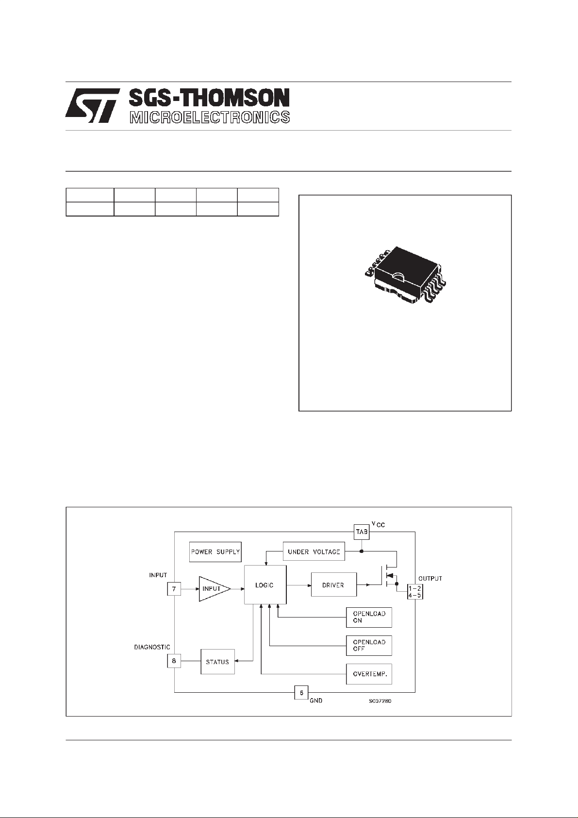
DESCRIPTION
The VN16BSP is a monolithic device made using
SGS-THOMSON Vertical Intelligent Power
Technology, intended for driving resistive or
inductiveloadswith one side grounded.
Built-in thermal shut-down protects the chip from
over temperatureand short circuit.
The open drain diagnostic output indicates: open
load in off stateand in on state, output shortedto
V
and overtemperature.
CC
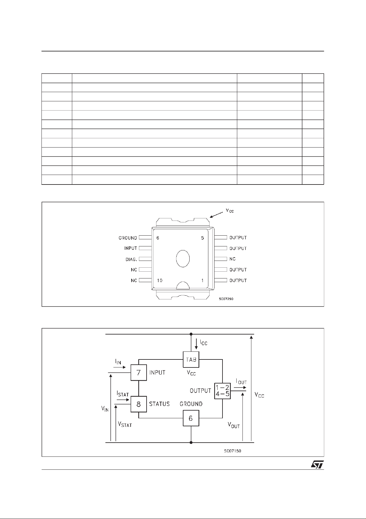
10
1
PowerSO-10
Fast demagnetization of inductive loads is
archivied by negative (-18V) load voltage at
turn-off
BLOCK DIAGRAM
March 1998
1/9
VN16BSP
ABSOLUTEMAXIMUMRATING
Symb o l Para met er Val u e Uni t
V
(BR)DSS
I
OUT
I
(RMS ) RMS O utput Current at Tc=85oC20A
OUT
I
I
-V
I
STAT
V
ESD
P
T
T
CONNECTIONDIAGRAMS
Drain-S o ur ce Br eakdown Volt age 40 V
Out put Cu r rent (cont. ) at Tc=85oC20A
Revers e Out put Curr ent at Tc=85oC (f > 1Hz) -20 A
R
Input Current ±10 mA
IN
Reverse Supply V oltage -4 V
CC
St at us Cur rent ±10 mA
Elect r o st at ic Dischar ge ( 1. 5 kΩ, 100 pF) 2000 V
Power Dissipation at Tc=25oC82W
tot
Junction Oper at in g T em pe r at ur e -40 t o 150
j
St orage Tem per at ure -55 t o 150
stg
o
C
o
C
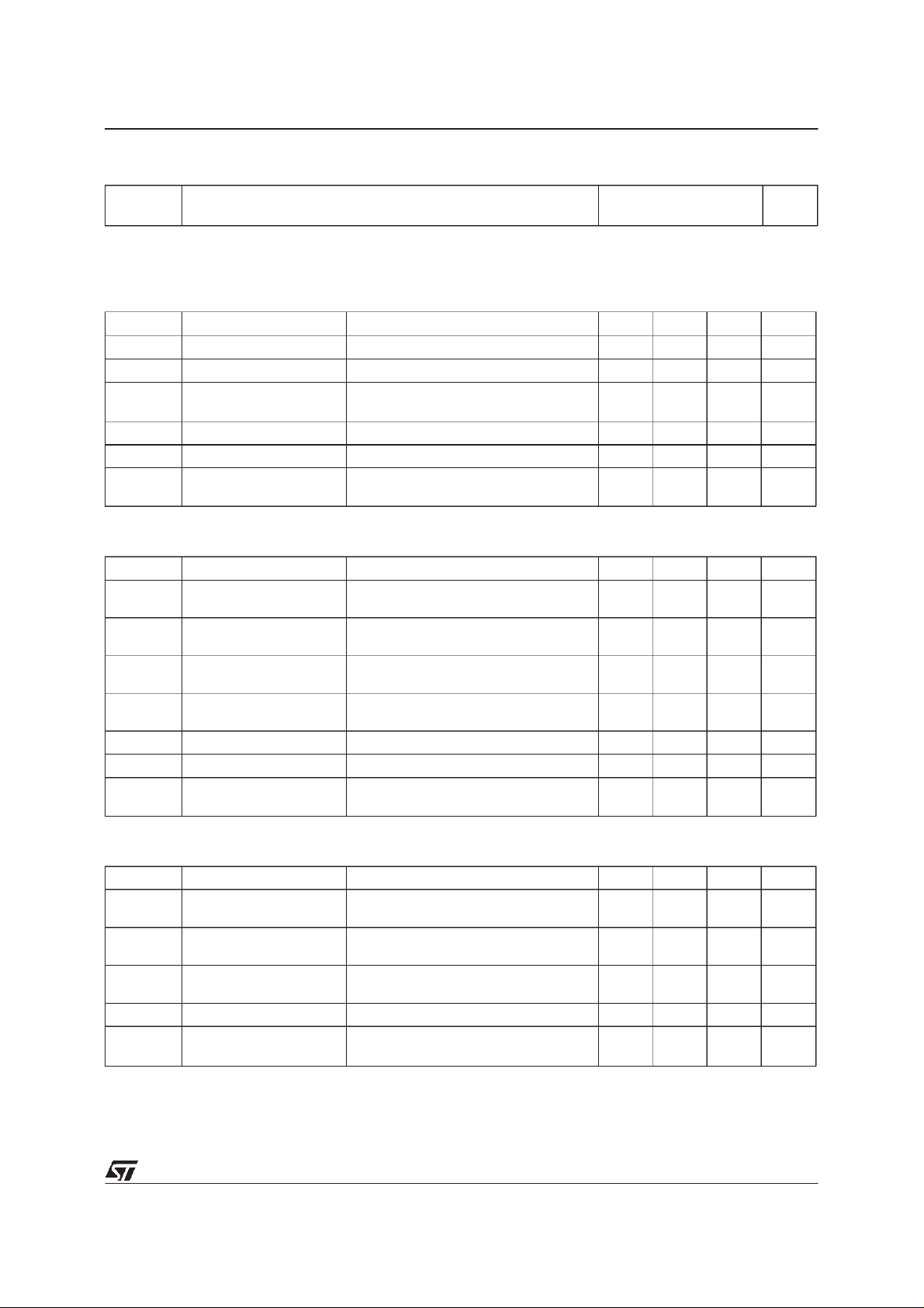
CURRENT AND VOLTAGECONVENTIONS
2/9
VN16BSP
THERMALDATA
R
thj-case
R
thj- amb
($) When mounted using minimum recommended pad size on FR-4 board
Ther mal Resis t ance Ju nct io n- case Max
Ther mal Resis t ance Ju nct io n- ambient ($) M ax
1.5
50
ELECTRICAL CHARACTERISTICS (8 < VCC< 16 V; -40 ≤ Tj≤ 125oC unless otherwisespecified)
POWER
Symbol Parameter Test C ondition s Min. Typ. Max. Unit
V
In(*) Nominal Current T
R
Supply Voltag e 6 13 26 V
CC
On Stat e Resist a nce I
on
=85oCV
c
=In VCC=13V Tj=25oC 0. 038 0.06 Ω
OUT
≤ 0.5 VCC=13V 5.6 8.8 A
DS(on)
o
o
C/W
C/W
I
V
DS(MAX)
R
Supply Current Of f Stat e VCC=13V Tj≥25oC2550µA
S
Maximum Voltage Drop I
Out put t o G ND Internal
i
=20A VCC=13V Tc=85oC1 1.8 V
OUT
Tj=25oC51020KΩ
Im pedance
SWITCHING
Symbol Parameter Test C ondition s Min. Typ. Max. Unit
t
(^) Turn-on D elay T im e Of
d(on)
R
=1.6Ω 550500µs
load
Out put Cu r rent
(^) Rise Time Of O utput
t
r
R
=1.6Ω 40 100 6 80 µs
load
Current
(^) Turn-off D elay Time Of
t
d(off)
R
=1.6Ω 10 100 5 00 µs
load
Out put Cu r rent
(^) Fall Time Of Output
t
f
R
=1.6Ω 40 100 6 80 µs
load
Current
(di/dt)
(di/dt)
V
demag
Tur n-on Current S lope R
on
Tur n-of f C urrent Slope R
off
Induc t i ve Load Clamp
=1.6Ω VCC= 13 V 0.008 0.1 A/ µs
load
=1.6Ω VCC= 13 V 0.008 0.1 A/ µs
load
R
=1.6Ω L=1mH -24 -18 -14 V
load
Volt age
LOGIC INPUT
Symbol Parameter Test C ondition s Min. Typ. Max. Unit
V
V
V
I(hyst.)
I
V
Input Low Level
IL
1.5 V
Volt age
Input Hig h Lev el
IH
3.5 (•)V
Volt age
Input Hysteresis
0.211.5V
Volt age
Input Current VIN=5V Tj=25oC100µA
IN
Input Cla m p Volt ag e IIN=10mA
ICL
I
=-10mA
IN
56
-0.7
7V
V
3/9
 Loading...