

VN16B
ISO HIGH SIDE SMART POWER SOLID STATE RELAY
PRELIMINARY DATA
TYPE V
VN16B 40 V 0.06 Ω 5.6 A 26 V
■ MAXIMUM CONTINUOUS OUTPUT
DSS
R
DS(on)
In(*) V
CC
CURRENT (#): 20 A @ Tc=85oC
■ 5V LOGIC LEVEL COMPATIBLEINPUT
■ THERMAL SHUT-DOWN
■ UNDER VOLTAGE PROTECTION
■ OPEN DRAIN DIAGNOSTIC OUTPUT
■ INDUCTIVELOADFAST DEMAGNETIZATION
■ VERYLOWSTAND-BY POWER DISSIPATION
DESCRIPTION
The VN16B is a monolithic device made using
SGS-THOMSON Vertical Intelligent Power
Technology, intended for driving resistive or
inductive loads with one side grounded.
Built-in thermal shut-down protects the chip from
over temperature and short circuit.
The open drain diagnostic output indicates: open
load in off state and in on state, output shorted to
VCCand overtemperature. Fast demagnetization
of inductive loads is archieved by negative (-18V)
load voltage at turn-off.
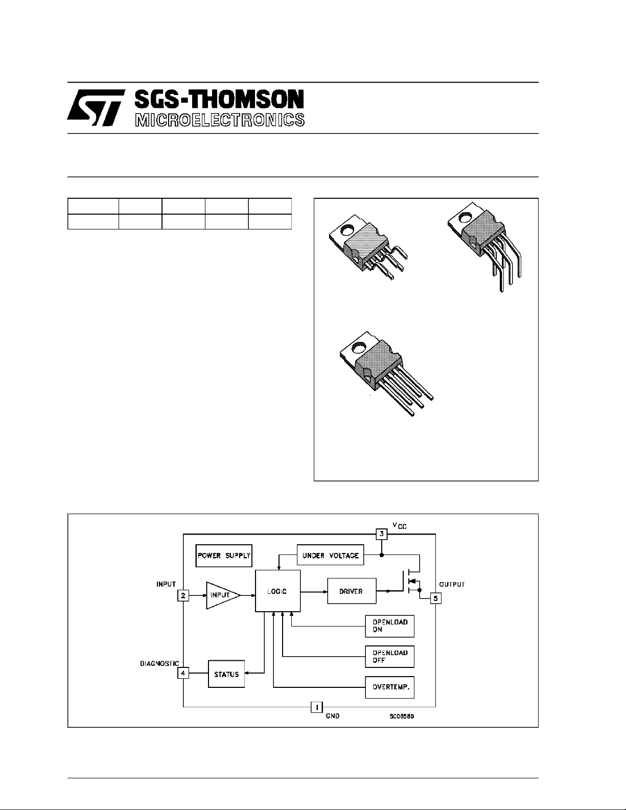
BLOCK DIAGRAM
PENTAWATT
(vertical)
PENTAWATT
(horizontal)
PENTAWATT
(in-line)
ORDER CODES:
PENTAWATT vertical VN16B
PENTAWATT horizontal VN16B (011Y)
PENTAWATT in-line VN16B (012Y)
(*) In= Nominal current accor ding to ISO defini t ion f or high side automoti ve swit ch (see note 1)
(#) The maximum conti nuous out put current i s the current at Tc=85oC for a battery voltage of 13 V whi ch does not ac tivate
sel f protection
September 1994
1/11

VN16B
ABSOLUTE MAXIMUM RATING
Symbol Parameter Value Uni t
V
(BR)DSS
I
OUT
(RMS ) RMS Output Cu rr ent at Tc=85oC20A
I
OUT
I
I
-V
I
STAT
V
ESD
P
T
T
CONNECTION DIAGRAM
Drain - So urc e Bre ak dow n Voltage 40 V
Out put Current (co nt . ) at Tc=85oC20A
Reverse Outpu t Cur r ent at Tc=85oC (f > 1Hz) -20 A
R
Input Curre nt ±10 mA
IN
Reverse S upply V olt age -4 V
CC
St at us Current ±10 mA
Electrost atic Dischar ge (1.5 kΩ , 100 pF ) 2000 V
Powe r Diss i pation at Tc=25oC82W
tot
Junction Op erating Temper at ur e -40 to 150
j
St or a ge Te mperat ur e -55 to 150
stg
o
C
o
C
CURRENT AND VOLTAGE CONVENTIONS
2/11

VN16B
THERMAL DATA
R
thj-case
R
thj-amb
Thermal Resis tance Junction - cas e Max
Thermal Resistance Junction - ambient Max
1.5
60
ELECTRICAL CHARACTERISTICS (8 < VCC< 16 V; -40 ≤ Tj≤ 125oC unless otherwise specified)
POWER
Symbol Parameter Test Condition s Min. Typ. Max. Unit
V
In( *) Nominal Curr ent T
R
Supply Voltage 6 13 26 V
CC
On State Resistance I
on
=85oCV
c
=In VCC=13V Tj=25oC 0.038 0.06 Ω
OUT
≤ 0.5 VCC=13V 5.6 8.8 A
DS(on)
o
o
C/W
C/W
I
V
DS(MAX)
R
Supply Current Of f S ta te VCC=13V Tj≥25oC2550µA
S
Maximum Volt age Drop I
Out put to GND I nternal
i
=20A VCC=13V Tc=85oC1 1.8 V
OUT
Tj=25oC51020KΩ
Im pedance
SWITCHING
Symbol Parameter Test Condition s Min. Typ. Max. Unit
(^) Tur n - on Delay T ime Of
t
d(on)
R
=1.6Ω 5 50 500 µ s
load
Out put Current
t
(^) Rise Ti m e Of Output
r
R
=1.6Ω 40 100 680 µs
load
Current
t
(^) T urn-off Delay Tim e Of
d(off)
R
=1.6Ω 10 100 500 µs
load
Out put Current
t
(^) Fall T ime Of Out put
f
R
=1.6Ω 40 100 680 µs
load
Current
(di/dt)
(di/dt)
V
demag
Turn-on C urrent S lope R
on
Turn-off Current Slope R
off
Inductive Load Clamp
=1.6Ω VCC= 13 V 0.008 0.1 A /µs
load
=1.6Ω VCC= 13 V 0.008 0.1 A /µs
load
R
=1.6Ω L = 1 mH -24 -18 -14 V
load
Volt age
LOGIC INPUT
Symbol Parameter Test Condition s Min. Typ. Max. Unit
V
IL
V
IH
V
I(hyst.)
I
IN
V
ICL
Input Low Level
Volt age
Input High Level
3.5 ( •)V
Volt age
Input Hys teresis
0.2 1 1.5 V
Volt age
Input Curre nt VIN=5V Tj=25oC 100 µA
Input Clamp Volta ge IIN=10mA
IIN=-10mA
56
-0.7
1.5 V
7V
V
3/11

VN16B
ELECTRICAL CHARACTERISTICS (continued)
PROTECTION AND DIAGNOSTICS(continued)
Symbol Parameter Test Condition s Min. Typ. Max. Unit
V
STAT
St at us Voltage Outp ut
Low
V
USD
Under V olt age Shut
Down
V
SCL
T
TSD
St at us Clamp Volt age I
Thermal Shut-down
Tem perature
T
SD( hyst.)
Thermal Shut-down
Hysteresis
T
V
I
OL
Reset T emperat ur e 125
R
Open Voltage Lev el Of f -S tate (note 2) 2.5 3.8 5 V
OL
Open Load Cur rent
Level
t
povl
t
pol
(*) In= Nominal current accor ding to ISO defini t ion f or high side automoti ve swit ch (see note 1)
(^) See Switchig Time Waveforms
(•)TheVIHis internal ly clamped at 6V about. It is possible to c onnect this pin to an higher voltage via an external r es istor
cal culated to not exceed 10 mA at the i nput pin.
note 1: The Nominal Cur rent is the current at Tc=85oC for battery voltage of 13V w hich produces a voltage drop of 0.5 V
note 2: I
note 3: t
St at us Delay (not e 3) 5 10 µs
St at us Delay (not e 3) 50 400 2500 µs
=(VCC-VOL)/ROL(see figure)
OL(off)
: ISO def inition (see figur e)
povltpol
I
=1.6mA 0.4 V
STAT
3.5 5 6 V
STAT
I
STAT
=10mA
=-10mA
56
-0.7
7V
140 1 60 180
15 50
On-State 0.15 0.85 A
V
o
C
o
C
o
C
Note 2 Relevant Figure Note 3 Relevant Figure
4/11
 Loading...