

SGS Thomson Microelectronics VN06SP Datasheet
®
HIGH SIDE SMART POWER SOLID STATE RELAY
TYPE V
DSS
VN06SP 60 V 0.18 Ω 1.9 A 26 V
■ MAXIMUM CONTINUOUS OUTPUT
CURRENT (#):9 A @ T
■ 5 V LOGIC LEVEL COMPATIBLE INPUT
■ THERMAL SHUT-DOWN
■ UNDER VOLTAG E PROT E CT ION
■ OPEN DRAIN DIAGNOSTIC OUTPUT
■ INDUCTIVE LOAD FAST
DEMAGNETIZATION
■ VERY LOW STAND-BY POWER
DISSIPATION
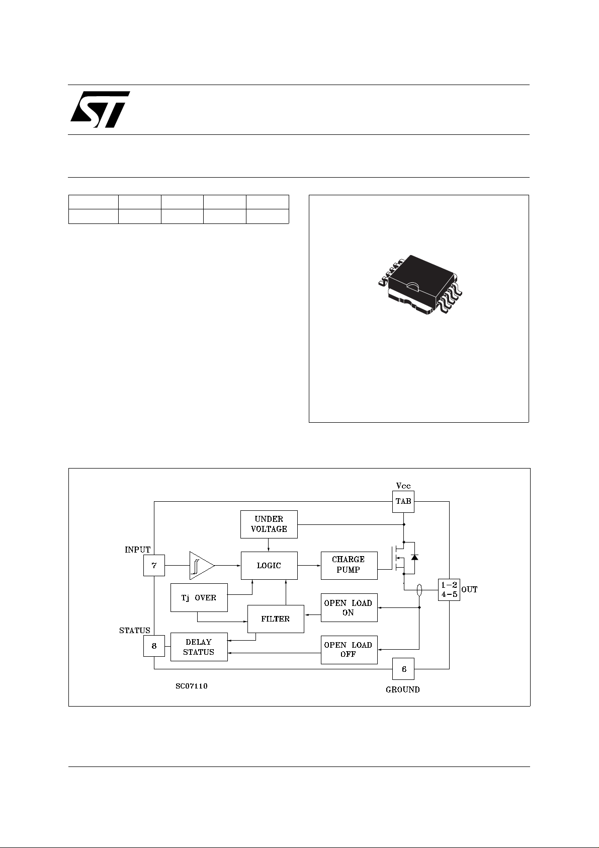
DESCRIP TION
The VN06SP is a monolithic device made using
STMicroelectronics VIPower Technology,
intended for driving resistive or inductive loads
with one side grounded.
Built-in thermal shut-down protects the chip from
over temperature and short circ uit.
The open drain diagnostic output indicates: open
load in off state, and in on state, output shorted to
R
DS(on)
=85oC
c
I
n(*)
V
CC
VN06SP
10
1
Powe r SO-10
V
and overtemperature. Fast demagnetization
CC
of inductive loads is archivied by negative (-18V)
load voltage at turn-off.
(*) In = Nominal current according to ISO definition for high side automotive switch (see note 1)
(#) The maximum continuous output current is the the current at T
protection.
= 85 oC for a battery voltage of 13V which does not activate self
c
July 1998
1/9
VN06SP
ABSOLUTE MAXIMUM RATING
Symbol Parameter Value Unit
V
(BR)DSS
I
OUT
I
I
-V
I
STAT
V
ESD
P
T
T
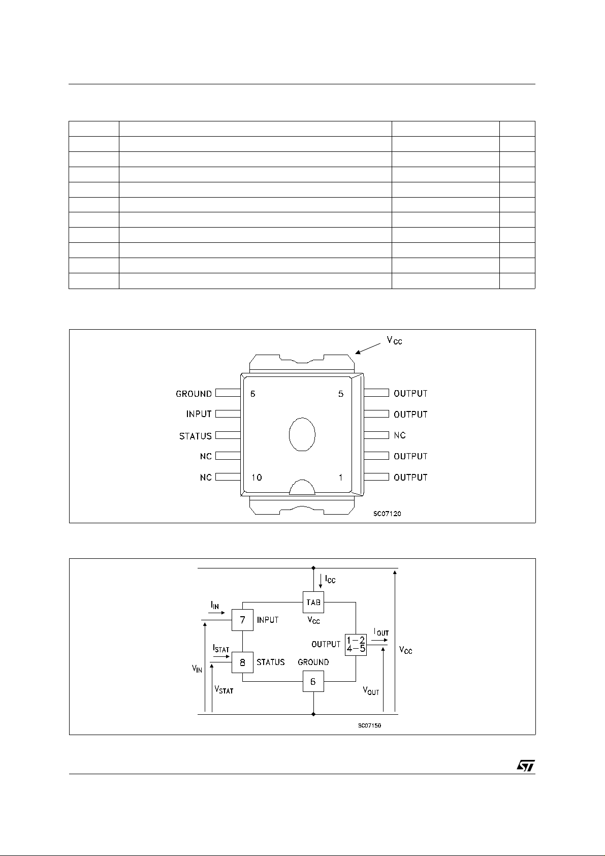
CONNECTION DIAGRAMS
Drain-Source Breakdown Voltage 60 V
Output Current (cont.) at Tc = 85 oC9A
Reverse Output Current at Tc = 85 oC-9A
R
Input Current ±10 mA
IN
Reverse Supply Voltage -4 V
CC
Status Current ±10 mA
Electrostatic Discharge (1.5 kΩ, 100 pF) 2000 V
Power Dissipation at Tc = 85 oC 27 W
tot
Junction Operating Temperature -40 to 150
j
Storage Temperature -55 to 150
stg
o
C
o
C
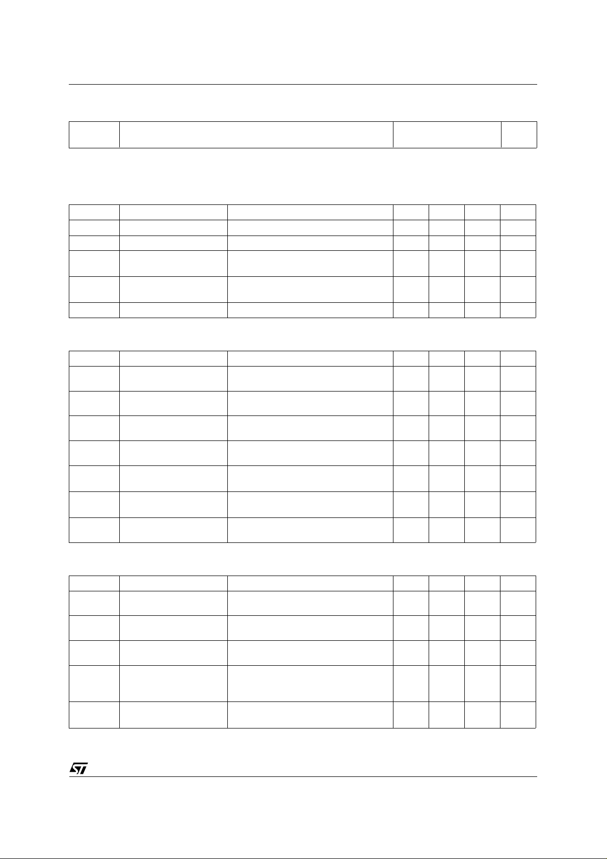
CURRENT AND VOLTAGE CONVENTI ONS
2/9
VN06SP
THERMAL DATA
R
thj-case
R
thj-amb
When mounted using minimum recommended pad size on FR-4 board
ELECTRICAL CHARACTERISTICS (VCC = 13 V; -40 ≤ Tj ≤ 125 oC unless otherwise specified)
POWER
Symbol Parameter Test Conditions Min. Typ. Max. Unit
V
In(*) Nominal Current Tc = 85 oC V
R
I
V
DS(MAX)
SWITCHING
Symbol Parameter Test Conditions Min. Typ. Max. Unit
t
d(on)
t
r
t
d(off)
t
f
(di/dt)
(di/dt)
V
demag
Thermal Resistance Junction-case Max
Thermal Resistance Junction-ambient Max
Supply Voltage 5.5 13 26 V
CC
On State Resistance I
on
Supply Current Off State Tj ≥ 25 oC
S
Maximum Voltage Drop I
(^) Turn-on Delay Time Of
Output Current
(^) Rise Time Of Output
Current
(^) Turn-off Delay Time Of
Output Current
(^) Fall Time Of Output
Current
Turn-on Current Slope I
on
Turn-off Current Slope I
off
Inductive Load Clamp
Voltage
2.4
50
≤ 0.5 (note 1) 1.9 A
DS(on)
= 1.9 A
OUT
I
= 1.9 A Tj = 25 oC
OUT
0.36
0.18
50
On State
= 8.5 A Tc = 85 oC 2.75 V
OUT
I
= 1.9 A Resistive Load
OUT
20 µs
15
Input Rise Time < 0.1 µs
I
= 1.9 A Resistive Load
OUT
20 µs
Input Rise Time < 0.1 µs
I
= 1.9 A Resistive Load
OUT
25 µs
Input Rise Time < 0.1 µs
I
= 1.9 A Resistive Load
OUT
6 µs
Input Rise Time < 0.1 µs
= 1.9 A
OUT
I
= IOV
OUT
= 1.9 A
OUT
I
= I
OUT
OV
I
= 1.9 A L = 1 mH -24 -18 -14 V
OUT
0.08 0.51A/µs
0.2 3
3
o
C/W
o
C/W
Ω
Ω
µA
mA
A/µs
A/µs
A/µs
LOGIC INP UT
Symbol Parameter Test Conditions Min. Typ. Max. Unit
V
V
V
I(hyst.)
I
V
IL
IH
IN
ICL
Input Low Level
Voltage
Input High Level
Voltage
Input Hysteresis
Voltage
Input Current VIN = 5 V
V
= 2 V
IN
V
= 0.8 V 25
IN
Input Clamp Voltage IIN = 10 mA
I
= -10 mA
IN
0.8 V
2(•)V
0.5 V
250 500
250
5.5 6
-0.7 -0.3
µA
µA
µA
V
V
3/9
 Loading...