

®
HIGH VOLTAGE IGNITION COIL DRIVER
■ NO EXTERNAL COMPONENT REQUIRED
■ INTEGRATED HIGH VOLTAGE CLAMP
■ COIL CURRENT LIMIT INTERNALLY SE T
■ HIGH RUGGEDNES S
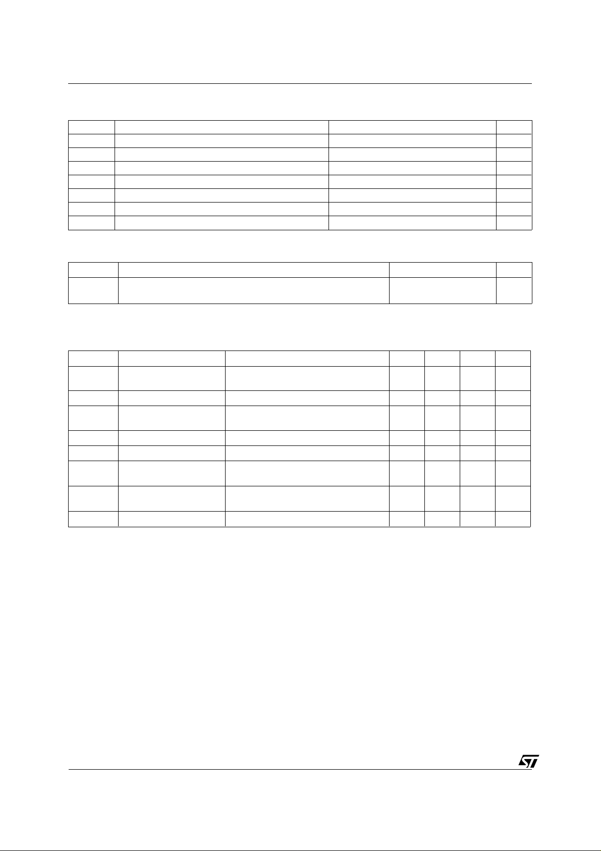
DESCRIPTION
The VB923 is a monolithic high voltage integrated
circuits made using STMicroelectronics VIPower
Technology, which combines a vertical current
flow power trilinton with a coil current limiting
circuit and a collector voltage clamping.
The device is peculiarly suitable for application in
high performance electronic car ignition, where
coil current limitation and voltage clamping are
required.
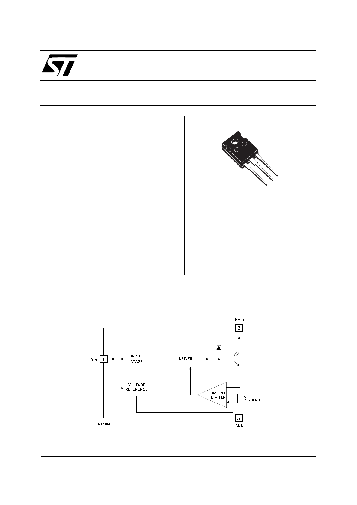
VB923
POWER IC
3
2
1
TO-247
BLOCK DIAG RAM
October 1998
1/5
VB923
ABSOLUTE MAXIMUM RATING
Symbol Parameter Value Unit
HV
P
T
E
THERMAL DATA
Symbol Parameter Value Unit
R
thj-case
R
thj-amb
Collector Voltage Internally Limited V
c
Collector Current Internally Limited A
I
c
Input Current 40 mA
I
in
Total Dissipation at Tc = 25 oC 150 W
tot
Storage Temperature -40 to 150
stg
Operating Junction Temperature -40 to150
T
j
Avalanche Energy 350 mJ
s/b
Thermal Resistance Junction-case Max
Thermal Resistance Junction-ambient Max
0.83
30
o
o
o
C/W
o
C/W
C
C
ELECTRICAL CHARACTERISTICS (V
= 14 V, HEI Coil = xx, T
batt
= 25 oC
case
unless otherwise specified)
Symbol Parameter Test Conditions Min. Typ. Max. Unit
I
cgo
V
V
cg(sat)
I
cl
V
f
V
inCL
V
inTH
t
d(off)
* ICL is measured 1ms after the maximum peak
** Pulsed: Pulse duration = 300 µs, duty cycle 1.5 %
Note 1: After adjusting input signal (frequency and duty) to be I
Note 2: The device is biased with 14V on collector with respectt o emitte r. Then a voltage ramp (0 to 5V) is put on input. V
voltage when the device is in on-stat e with I
Collector Cut-off
Vin = 0 HVc = 200 V 250 µA
Current
Clamping Voltage -40 < Tj < 125 oC Ic = 5 A 350 400 500 V
cl
Power Stage
Ic = 5 A Vin = 4 V 2 2.5 V
Saturation Voltage
* Coil Current Limit
-30 ≤ T
≤ 50 oC
j
6.0 6.6 7.2 A
** Diode Forward Voltage If = 10 A 3.5 V
Input Voltage During
On State
Threshold Input
Voltage
-30 ≤ T
I
-30 ≤ T
≤ 120 oC Ic = 5 A
j
= 10 mA see note 1
in
≤ 120 oC Ic = 5 A
j
see note 2
0.5 4 V
4V
Switching Time Ic = 3 A L = 6 mH (see fig.1) 15 40 µs
= 5A, Vin (Tr ON) should be measured.
C
C
=5A
is the input
inTH
2/5
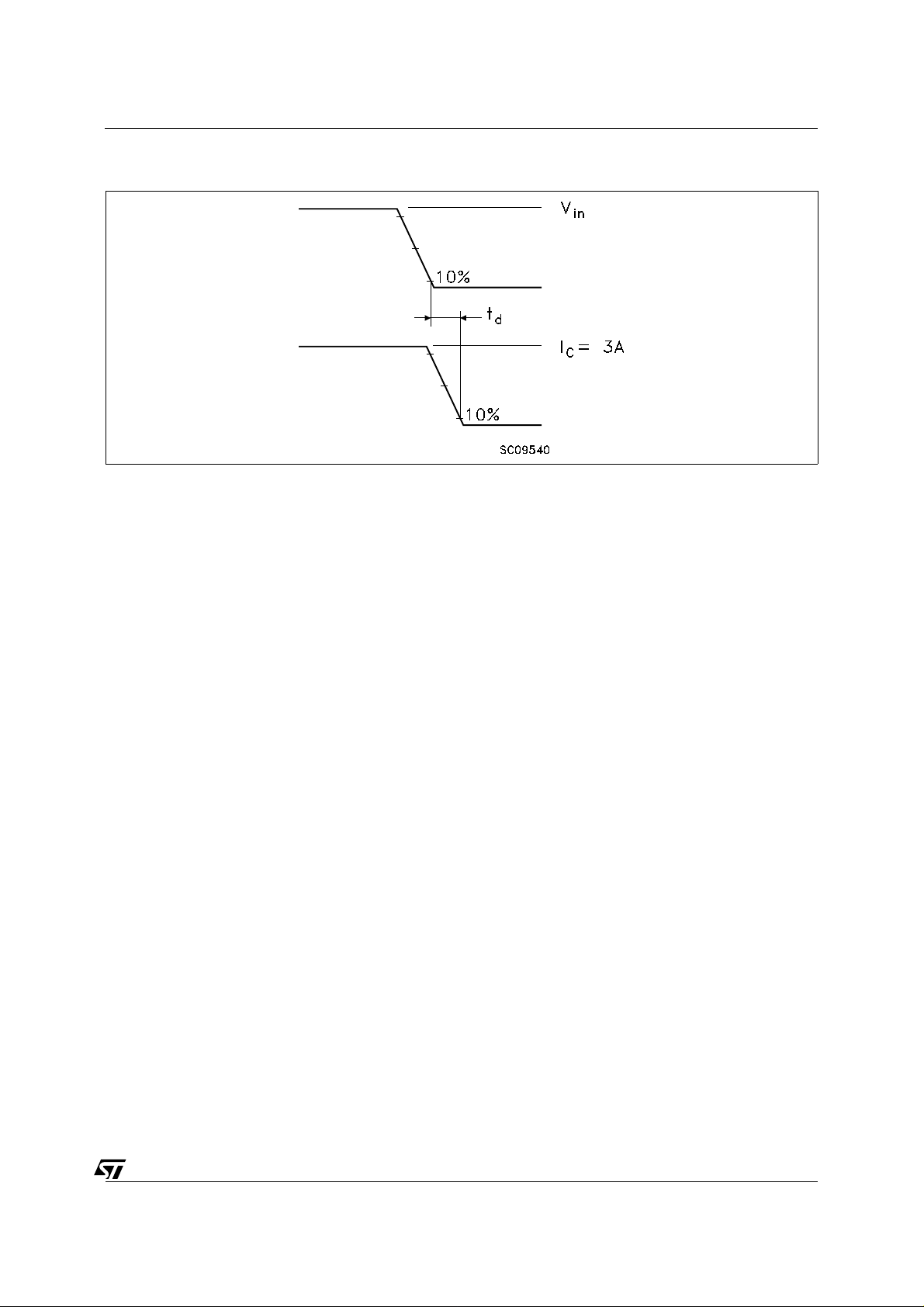
Fig. 1 Switching Time
VB923
3/5
VB923
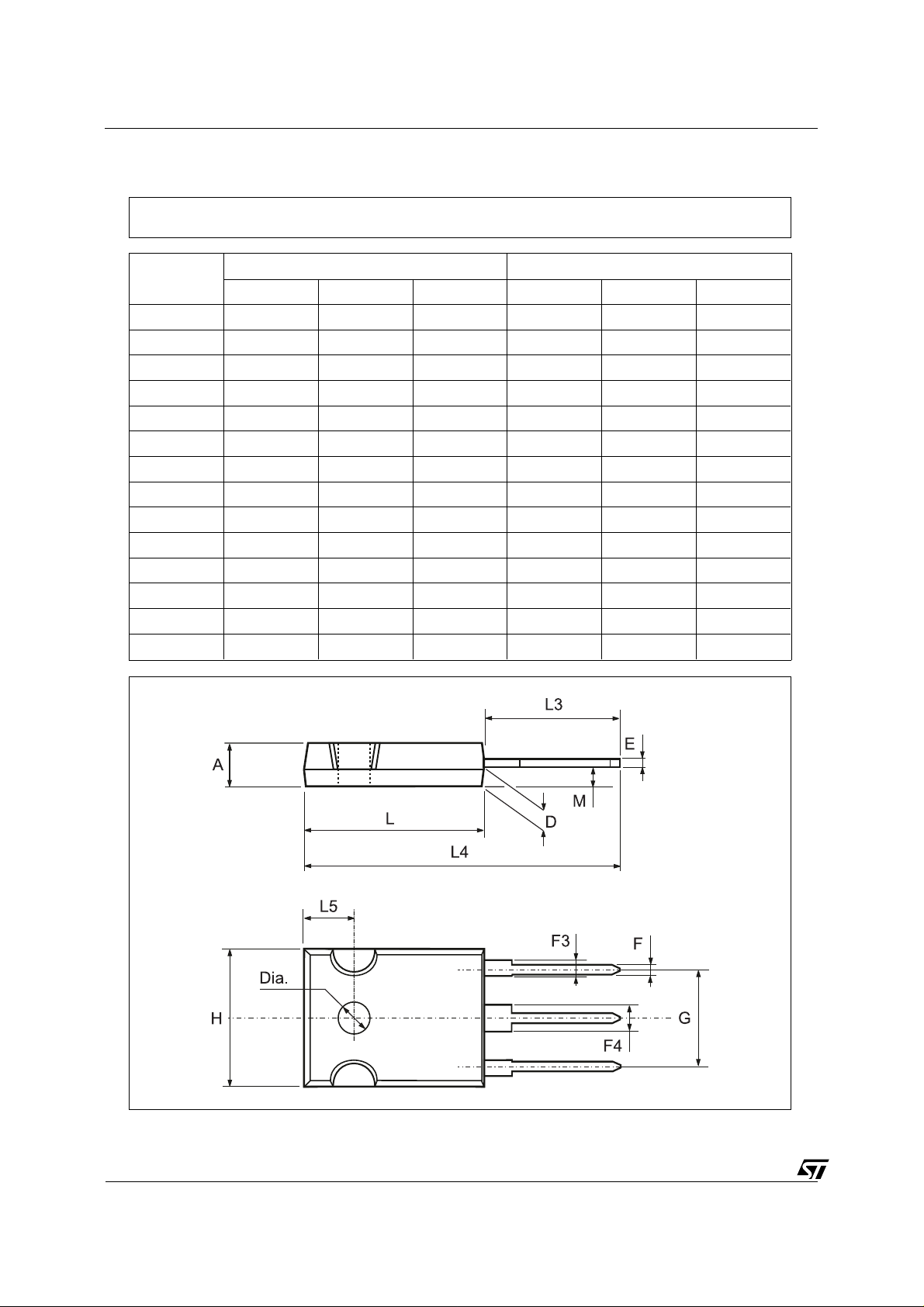
TO-247 MECHANICAL DATA
DIM.
MIN. TYP. MAX. MIN. TYP. MAX.
A 4.7 5.3 0.185 0.209
D 2.2 2.6 0.087 0.102
E 0.4 0.8 0.016 0.031
F 1 1.4 0.039 0.055
F3 2 2.4 0.079 0.094
F4 3 3.4 0.118 0.134
G 10.9 0.429
H 15.3 15.9 0.602 0.626
L 19.7 20.3 0.776 0.779
L3 14.2 14.8 0.559 0.413 0.582
L4 34.6 1.362
L5 5.5 0.217
M 2 3 0.079 0.118
Dia 3.55 3.65 0.140 0.144
mm inch
4/5
P025P

VB923
Information furnished is believed to be accurate and reliable. However, STMicroelectronics assumes no responsibility for the consequences
of use of such inform ation nor for any infringe ment o f patents or other rig hts o f third par ties which ma y resul t from i ts use. N o li cen se is
granted by implicatio n or otherwise under any patent or patent rights of STMicroelectronics. Specification mentioned in this publication are
subject to change without notice. This publication supersedes and replac es all information previously supplied. STMicroelectronics products
are not authorized for use as critical compo nents in life support devices or systems without express written approval of STMicroelectronics.
The ST logo is a registered trademark of STMicroelectronics
© 1998 STMicroelectro nics – Printed in Italy – All Rights Reserved
STMicroelectronics GROUP OF COMPANIES
Australia - Brazil - Canada - China - France - Germany - Italy - Japan - Korea - Malaysia - Malta - Mexico - Morocco - The Netherlands -
Singapore - Spain - Sweden - Switzerland - Taiwan - Thailand - United Kingdom - U.S.A.
http://www.st.com
.
5/5
 Loading...