

VB029 / VB029SP
HIGH VOLTAGE IGNITION COIL DRIVER
/ VB029(011Y)/ VB029(012Y)
POWER I.C.
TYPE V
VB029
VB029SP
VB029(011Y)
VB029(012Y)
■ PRIMARY COIL VOLTAGE INTERNALLY SET
■ COIL CURRENTLIMIT INTERNALLY SET
■ LOGIC LEVEL COMPATIBLE INPUT
■ DRIVING CURRENTQUASI PROPORTIONAL
cl
320V 12A 230mA
I
cl
I
d(on)
TO COLLECTOR CURRENT
■ DOUBLE FLAG-ONCOIL CURRENT
■ DARLINGTON BASE ACCESSIBLE
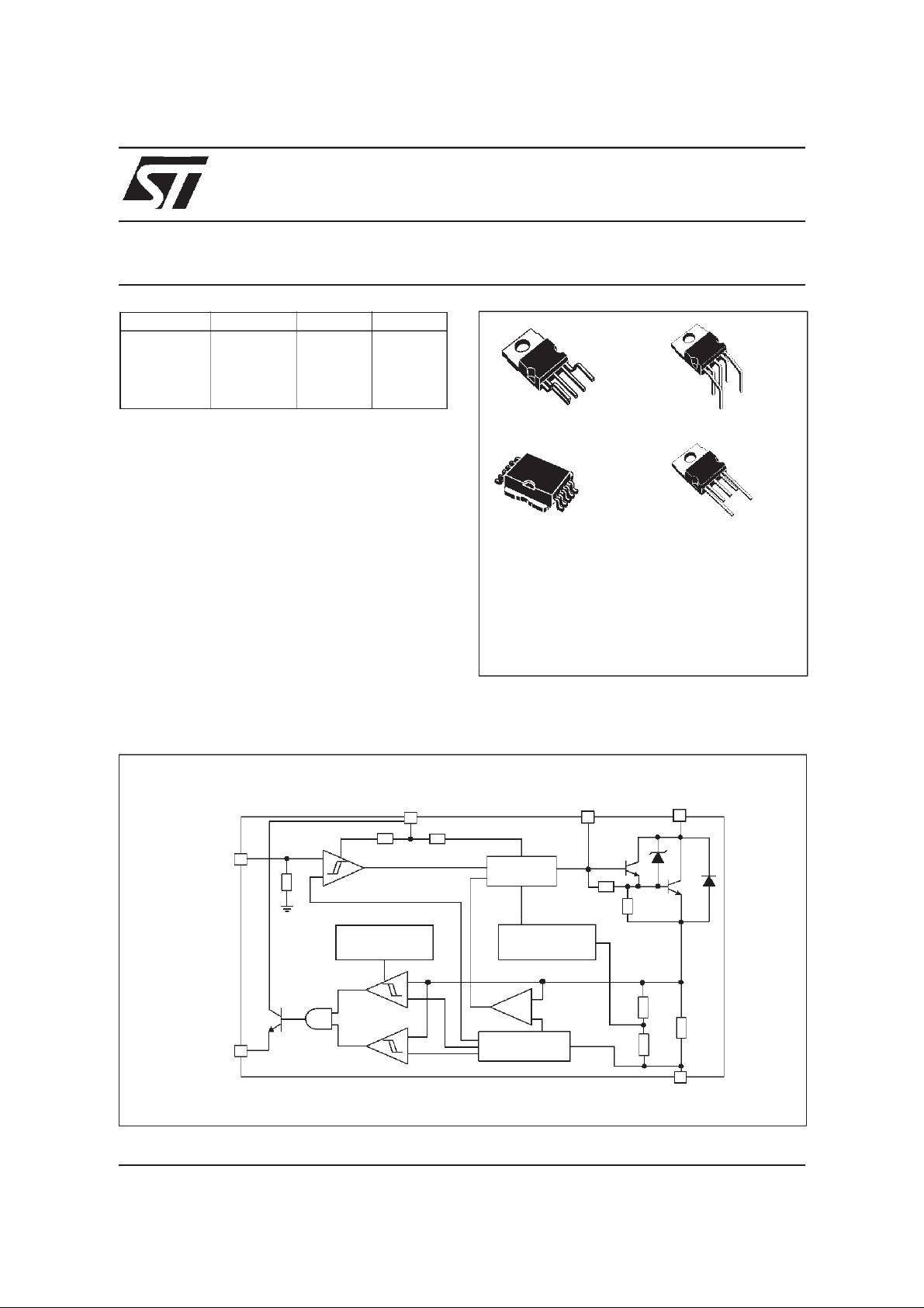
DESCRIPTION
The VB029, VB029SP, VB029(011Y)
VB029(012Y) are a high voltage power integrated
circuit designed in STMicroelectronics VIPower
technology, with vertical current flow power
darlington and logic level compatible driving
circuit. Built-in protection circuit for coil current
limiting and collector voltage clamping allows the
device to be used as smart, high voltage, high
BLOCK DIAGRAM
PENTAWATT HV PENTAWATT HV (011Y)
10
1
PowerSO-10
PENTAWATT HV (012Y)
ORDER CODES:
PowerSO-10
PENTAWATTHV
PENTAWATTHV (011Y)
PENTAWATTHV (012Y)
VB029SP
VB029
VB029(011Y)
VB029(012Y)
current interface in advanced electronic ignition
system.
V
d
INPUT
OVERTEMP.
PROTECTION
DIAG 1
DIAG
July 1999 1/10
DIAG 2
+
-
-
+
DRIVER
QUASI PROP.
BASE CURRENT
REFERENCE
V
base
HV
GND
C
R
SENSE
VB029 / VB029SP / VB029(011Y) / VB029(012Y)
ABSOLUTE MAXIMUM RATING
Symbol Parameter Value Unit
HV
I
V
I
V
T
T
THERMAL DATA
Symbol Parameter
R
thj-case
R
thj-amb
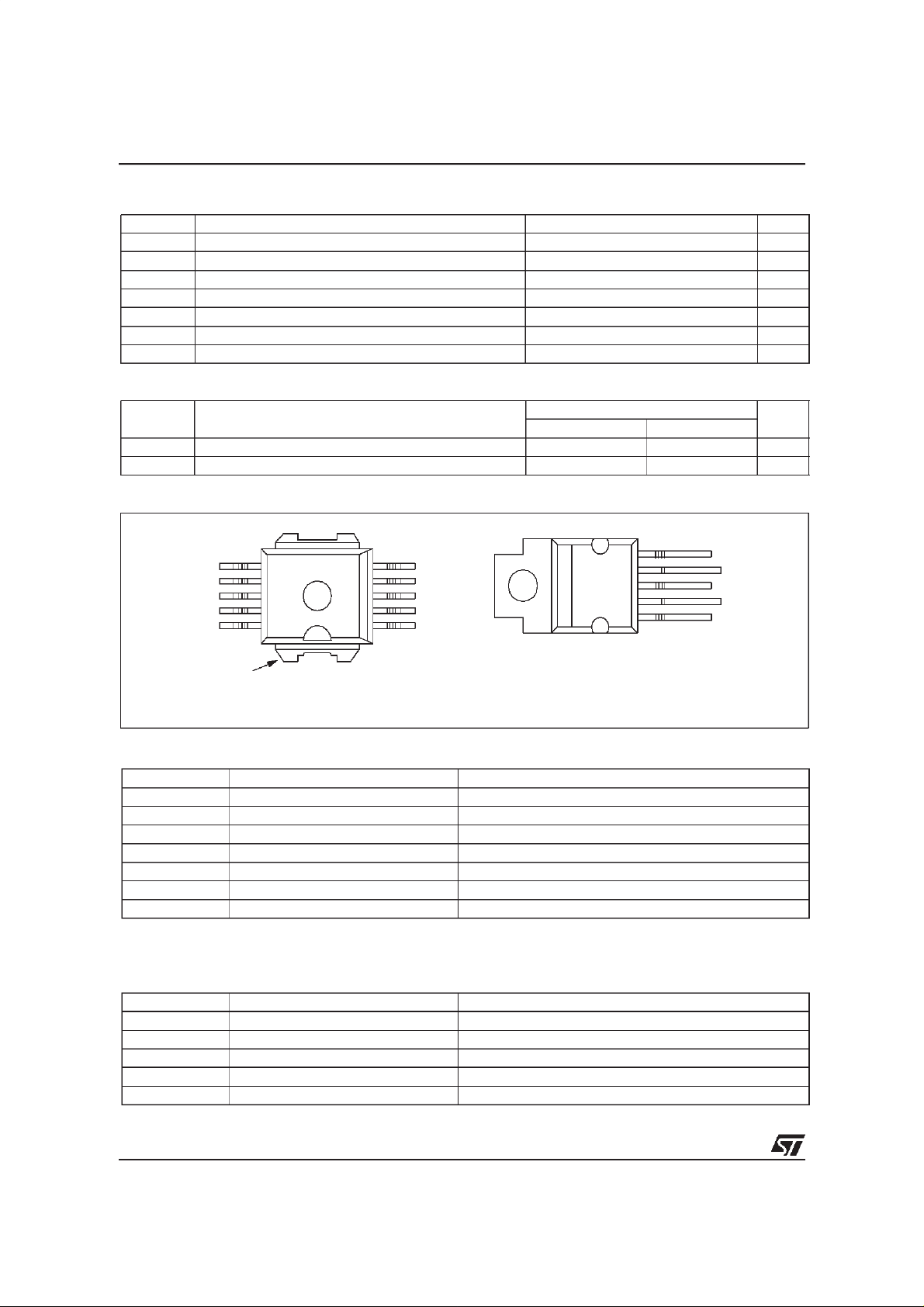
CONNECTION DIAGRAM (TOPVIEW)
Collector voltage Internally limited V
c
Collector current Internally limited A
C
Driving stage supply voltage 7 V
d
Driving circuitry supply current 230 mA
d
Input voltage 10 V
IN
Junction operating temperature -40 to 150 °C
j
Storage temperature -55 to 150 °C
stg
Value
PowerSO-10 PENTAWATT HV
Thermal resistance junction-case (MAX) 1.12 1.12 °C/W
Thermal resistance junction-ambient (MAX) 62.5 62.5 °C/W
Unit
BASE
GND
V
d
INPUT
DIAG
6
7
8
9
10
11
HV
C
PowerSO-10
5
4
3
2
1
GND
GND
GND
GND
GND
PENTAWATT HV
PENTAWATT HV (011Y)
PENTAWATT HV (012Y)
PIN FUNCTION (PowerSO-10)
No Name Function
1÷5 GND Emitter power ground
6 BASE Darlington base
7(*) GND Control ground
8V
d
Driving stage supply voltage
9 INPUT Logic input channel
10 DIAG Diagnostic output signal
TAB HV
(*) Pin 1÷5=Power GND, Pin 7=signal GND. Pin 7 must be connected to pins 1÷5 externally.
C
Primary coil output signal
PIN FUNCTION (PENTAWATT HV)
No Name Function
1 GND Emitter power ground
2V
3HV
d
C
4 INPUT Logic input channel
5 DIAG Diagnostic output signal
Driving stage supply voltage
Primary coil output signal
5
4
3
2
1
DIAG
INPUT
HV
C
V
d
GND
2/10
1
VB029 / VB029SP / VB029(011Y) / VB029(012Y)
ELECTRICAL CHARACTERISTICS (V
specified)
=13.5V; Vd=5V; Tj=25ºC; R
CC
coil
=510m
Ω;
L
=7mH unless otherwise
coil
Symbol Parameter Test Conditions Min Typ Max Unit
V
V
cg(sat)td
I
d(off)
I
d(on)
V
I
V
INH
V
I
INH
V
diagH
V
diagL
I
C(diag1)
INL
High voltage clamp -40°C≤Tj≤125°C; IC=6A 320 360 420 V
cl
Power stage saturation
voltage derating in
temperature
=7.6A; VIN=4V; -40°C≤Tj≤80°C
I
C
IC=7.6A; VIN=4V; 80°C≤Tj≤125°C
Power-off supply current VIN=0.4V 10 mA
Power-on supply current VIN=4V; IC=7.6A; -40°C≤Tj≤125°C 230 mA
Driving stage supply
d
voltage
Collector current limit VIN=4V; -40°C≤Tj≤125°C;(See note 1) 12 A
cl
4.5 5.5 V
High level inputvoltage 4 5.5 V
Low level input voltage 0 0.8 V
High level inputcurrent VIN=4V 200 µA
High level diagnostic
output voltage
Low level diagnostic
output voltage
First threshold level
collector current
R
=22KΩ (See figure 1) 3.5 (*) V
EXT
=22KΩ (See figure1) 0.5 V
R
EXT
2.15 2.5 2.85 A
2.5
2.8
d
First threshold level
I
C(diag1)td
I
C(diag2)
collector current drift with
temperature
Second threshold level
collector current
(See figure 3)
6.1 6.5 6.9 A
Second threshold level
I
C(diag2)td
collector current drift with
(See figure 4)
temperature
t
d(off)
t
f(off)
t
d(diag)
t
r(diag)
t
f(diag)
∆I
E
Turn-off delay time of
output current
Turn-off fall time ofoutput
current
Delay time of diagnostic
current
Turn-on rise time of
diagnostic current
Turn-off fall time of
diagnostic current
Thermal flag shift on first
th
threshold
Single pulse avalanche
s/b
energy
IC=6A (See note 2) 25 µs
IC=6A 8 µs
R
=22KΩ (See figure1) 1 µs
EXT
=22KΩ (See figure1) 1 µs
R
EXT
R
=22KΩ (See figure1) 1 µs
EXT
Tj>125°C (**) 1 A
300 mJ
V
V
V
Note 1: theprimary coil current value Iclmust be measured 1ms after desaturation of the power stage.
Note 2: timefrom input switching V
(*) Vd-V
be(on)
(**) This thermal flag shift cannot be activated for lower than 125°C.
until collector voltage equal to 200V.
NEG
3/10
1
 Loading...