

SGS Thomson Microelectronics USBDF02W5, USBDF01W5 Datasheet
®
EMI FILTER AND LINE TERMINATION
A.S.D.
APPLICATIONS
EMI Filter and line termination for USB downstream ports on:
- Desktop computer
- Notebooks
- Workstations
- USB Hubs
FEATURES
Monolithic device with recommended line termi-
n
nation for USB downstream ports
Integrated Rt series termination and Ct bypass-
n
ing capacitors.
Integrated ESD protection
n
Small package size
n
DESCRIPTION
The USB specification requires USB
downstream ports to be terminated with
pull-down resistors fromthe D+ and D- lines to
ground. On the implementation of USB
systems, the radiated and conducted EMI
should be kept within the required levels as
stated by the FCC regulations. In addition to
the requirements of termination and EMC
compatibility, the computing devices are
required to be tested for ESD susceptibility.
The USBDFxxW5 provides therecommended line
termination while implementing a low pass filter to
limit EMI levels and providing ESD protection
which exceeds IEC 61000-4-2 level 4 standard.
The device is packaged in a SOT323-5L which is
the smallest available lead frame package (50%
smaller than the standard SOT23).
BENEFITS
n
EMI / RFI noise suppression
n
Required line termination for USB downstream
ports
n
ESDprotectionexceeding IEC61000-4-2 level4
n
High flexibility in the design of high density
boards
n
Tailored to meet USB 1.1 standard
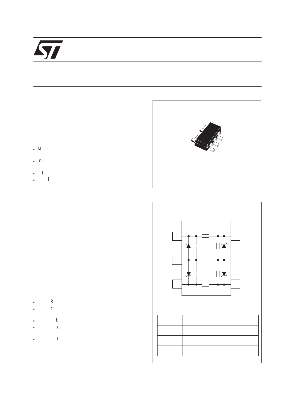
FOR USB DOWNSTREAM PORTS
USBDFxxW5
SOT323-5L
FUNCTIONAL DIAGRAM
D+ In
Gnd
D- In
Code 01 33Ω 15kΩ 47pF
Code 02 15Ω 15kΩ 47pF
Rt
Ct
Rd
Rd
Ct
Rt
Rt Rd Ct
D+ Out
D- Out
TM: ASDandTRANSIL are a trademarks of STMicroelectronics.
May 2000 Ed : 1C
Tolerance ±10% ±10% ±20%
1/9

USBDFxxW5
COMPLIES WITH THE FOLLOWING ESD
STANDARDS:
IEC-61000-4-2, level 4
±15 kV (air discharge)
±8 kV (contact discharge)
MIL STD 883C, Method 3015-6
Class 3 C = 100 pF R = 1500 Ω
3positivestrikes and 3negative strikes (F=1Hz)
ABSOLUTE MAXIMUM RATINGS (T
amb
= 25°C)
Symbol Parameter Value Unit
V
PP
ESD discharge IEC 61000-4-2, contact discharge
ESD discharge - MIL STD 883 - Method 3015-6
T
j
T
stg
T
L
T
op
P
r
Junction temperature
Storage temperature range
Lead solder temperature (10 second duration)
Operating temperature Range
Power rating per resistor
ELECTRICAL CHARACTERISTICS (T
amb
= 25°C)
±15
±25
150 °C
- 55 to +150 °C
260 °C
0to70 °C
100 mW
Symbol Parameters Testconditions Min Typ Max Unit
V
BR
V
F
Diode breakdown voltage IR= 1mA
Diode forward voltage drop IF= 50mA
6V
0.9 V
kV
kV
2/9
APPLICATION INFORMATION
Fig. A1: USB Standard requirements
Full-speed or
Low-speed USB
Transceiver
Host or
Hub port
Full-speed or
Low-speed USB
Transceiver
Host or
Hub port
Rt
Ct
Rt
15k
Ct
Rt
Ct
Rt
15k
Ct
15k
15k
D+
Twisted pair shielded
D-
D+
D-
Zo = 90ohms
5m max
FULL SPEED CONNECTION
Untwisted unshielded
3m max
LOW SPEED CONNECTION
D+
D-
D+
D-
+Vbus
1.5k
+Vbus
1.5k
Rt
Ct
Rt
Ct
Rt
Ct
Rt
Ct
Full-speed USB
Transceiver
Hub 0 or
Full-speed function
Low-speed USB
Transceiver
Hub 0 or
Low-speed function
USBDFxxW5
APPLICATION EXAMPLE
Host/Hub USB
port transceiver
USBDF
xxW5
Upstream portDownstream port
D+ (1)
CABLE
D+
D-
(1) for a low-speed port
(2) for a full-speed port
D- (2)
+Vbus
D- (1)
D+ (2)
USBUF
xxW6
Peripheral
transceiver
3/9
 Loading...