SGS Thomson Microelectronics USB6B1 Datasheet

®
Application Specific Discretes
A.S.D.
APPLICATIONS
Where transient overvoltage protection in sensitive equipment is required, such as:
- Universal Serial Bus ports
- RS-423 interfaces
- RS-485 interfaces
- ISDN equipment
- T1/E1 line cards
- HDSL / ASDL interfaces
USB6Bx
DATA LINES PROTECTION
FEATURES
Full diode bridge with integrated clamping protection
n
Breakdown voltage : VBR = 6V min.
n
Peakpulsepower dissipation :PPP=500W(8/20µs)
n
Very low capacitance, compatible with high debit
n
data or signal rates.
DESCRIPTION
In order to prevent fast transients from leading
to severe damages in a high speed data system, a specific protection has been developed
by STMicroelectronics.
The USB6Bx protects the two input lines
against overvoltage. Besides, this device also
keeps the power rails in a safe limit thanks to
the integrated Transil diode.
BENEFITS
n
Provides protection for each line and between
the supply voltage and GND : 25A , 8/20µs.
n
High ESD protection level : up to level 3 per
MIL STD 883C-Method 3015-6
n
Separated inputs and outputs (so-called 4-point
structure) to improve ESD susceptibility.
n
Comprehensive package pin-out for immediate
implementation.
COMPLIES WITH THE FOLLOWING STANDARDS:
MIL STD 883C - Method 3015-6
class 3 C = 100 pF R= 1500 Ω
3 positive strikes and 3 negative strikes (F=1Hz)
IEC-1000-4-2 level 4
15 kV (air discharge)
8 kV (contact discharge)
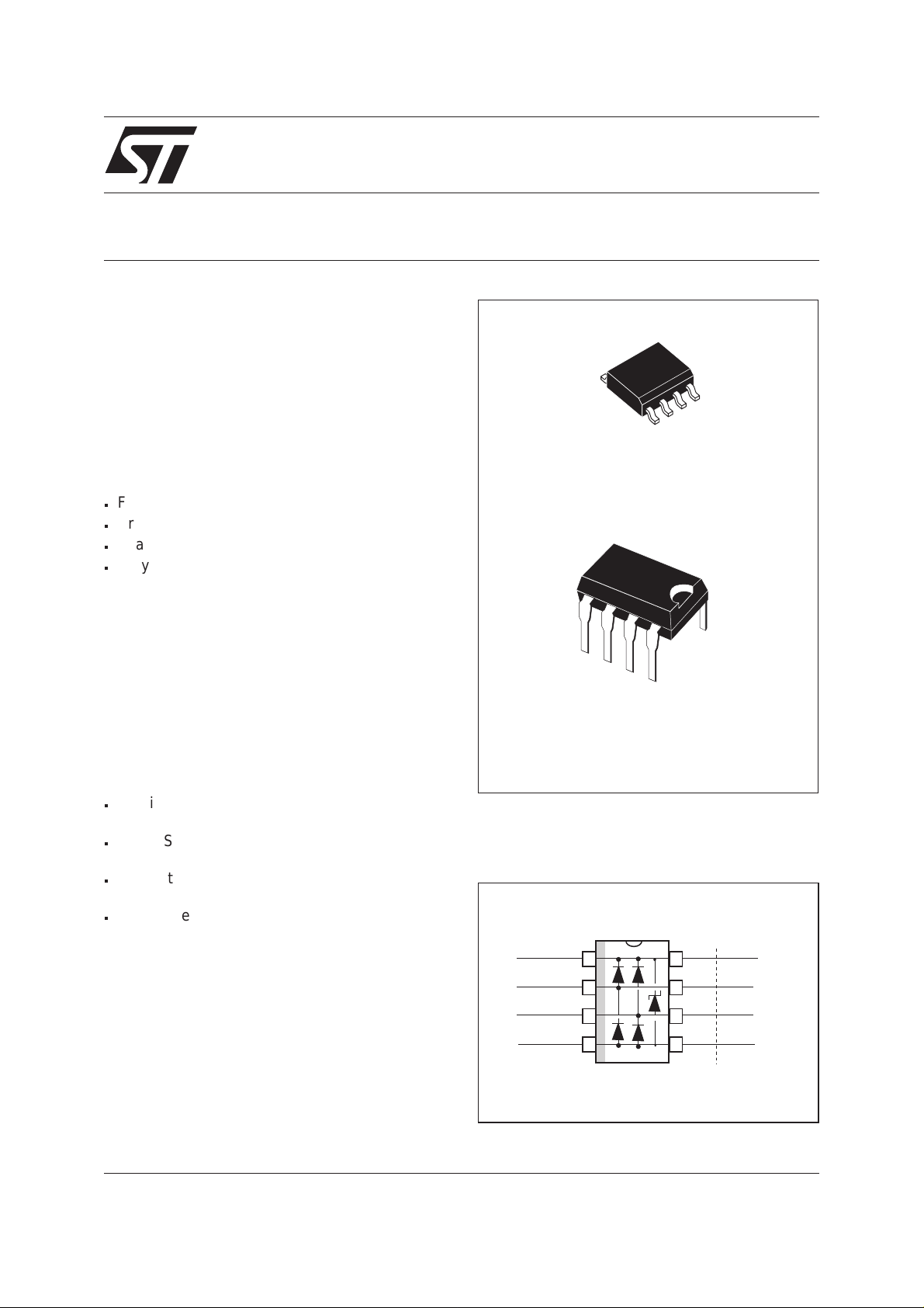
SO8
DIL8
FUNCTIONAL DIAGRAM
Vcc
I/01
I/02
GND
Vcc
I/01
I/02
GND
TM: ASDandTRANSIL are trademarks of ST Microelectronics.
August 1999 Ed : 5A
1/9

USB6Bx
TECHNICAL INFORMATION
SURGE PROTECTION
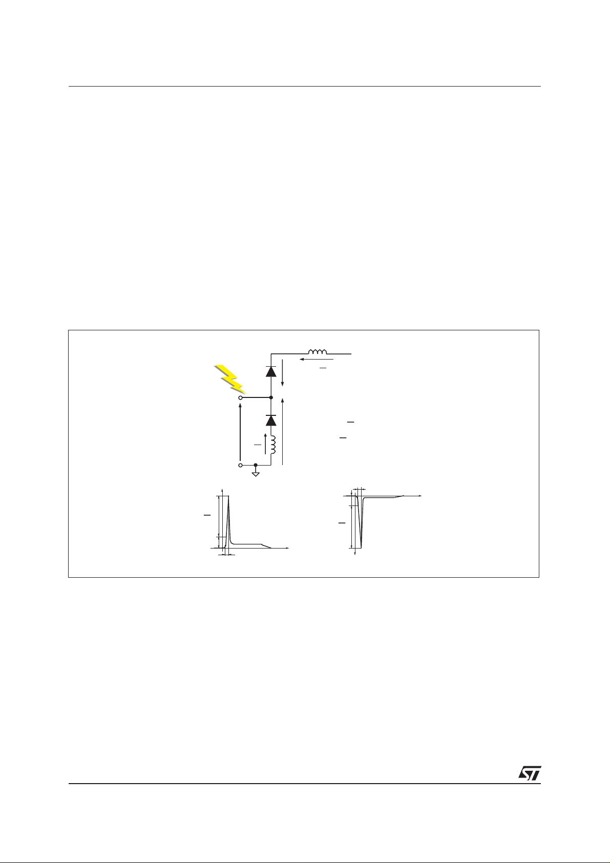
The USB6Bx is particularly optimized to perform
surge protection based on the rail to rail topology.
Theclampingvoltage VCLcanbeestimated as follow:
+=Vcc+VFfor positive surges
V
CL
V
CL
-=-V
for negative surges
F
F=Vt
+ rd.Ip
with: V
(V
forward drop voltage) / (Vtforward drop
F
threshold voltage)
Note: the estimations do not take into account
phenomena due to parasitic inductances.
Fig. A1 :
ESD
SURGE
I/O
Lw
Vcc+Vf
VI/O
di
dt
tr=1ns
Vcl+
di
Lw
dt
POSITIVE
SURGE
GND
Vf
Vcl+ =
Vcl- =
t
Lw
di
Lw
dt
Vcc+Vf+
-Vf-
-Lw
Lw
Lw
-Vf
+Vcc
di
surge >0
dt
di
surge <0
dt
tr=1ns
t
NEGATIVE
di
SURGE
dt
Vcl-
2/9

USB6Bx
HOW TO ENSURE A GOOD ESD PROTECTION
While the USB6Bx provides a high immunity to
ESD surge, an efficient protection depends on the
layoutofthe board. Inthesame way, withtherail to
rail topology, the track from the V
pin to the
CC
power supply and from the GND pin to GND voltage must be as short as possible to avoid
overvoltages due to parasitic phenomena (see Fig
A1).
It’s often harder to connect the power supply near
to the USB6Bx unlike the ground thanks to the
ground plane that allows a short connection.
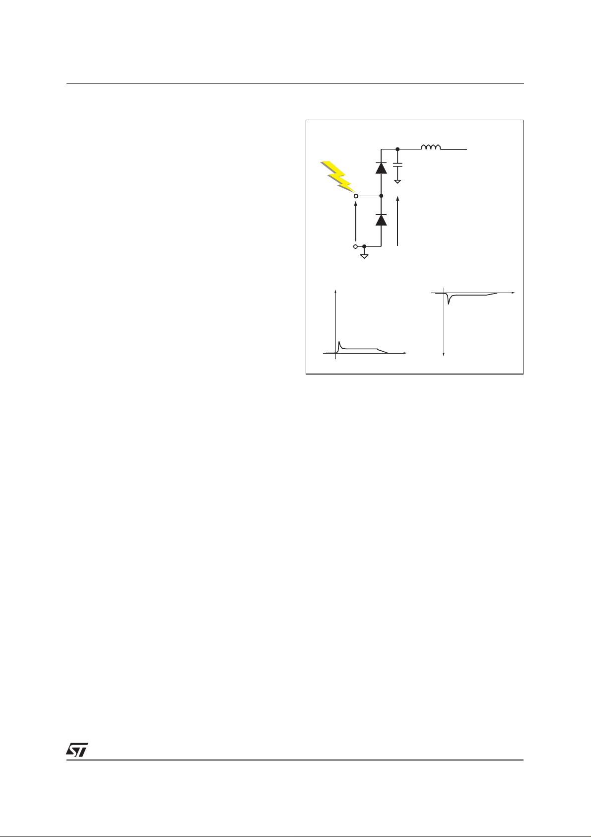
To ensure the same efficiency for positive surges
when the connections can’t be short enough, we
recommend to put close to the USB6Bx between
and ground, a capacitance of 100nF to pre-
V
CC
vent from these kinds of overvoltage disturbances
(see Fig. A2 ).
The add of this capacitance will allow a better protection by providing during surge a constant voltage.
Fig. A3 shows the improvement of the ESD protection according to the recommendations described above.
Fig. A2: ESD behavior: optimized layout and add
of a capacitance of 100nF.
C=100nF
Vcl+ =
Vcl- =
t
Lw
Vcc+Vf
-Vf
REF2=+Vcc
surge >0
surge <0
NEGATIVE
SURGE
Vcl-
ESD
SURGE
I/O
VI/O
REF1=GND
Vcl+
POSITIVE
SURGE
IMPORTANT:
A main precaution to take is to put the protection
device closer to the disturbance source (generally
the connection).
t
3/9
