

SGS Thomson Microelectronics UPSD3212CV, UPSD3212C, UPSD3212 Datasheet
Flash Programmabl e System Dev i c es
with 8032 Microcontroller Core and 16Kbit SRAM
FEATURES SUMMARY
■ The uPSD321X Devices combine a Flash PSD
architecture with an 8032 microcontroller core.
The uPSD321X Devices of Flas h PSDs feat ure
dual banks of Flash memory, SRAM, general
purpose I/O and programmable logic, supervisory functions and access via I
PWM channels, and an on-board 8032 microcontroller core, with two UARTs, three 16-bit
Timer/Counters and two External Interrupts. As
with other Flash PSD families, the uPSD321X
Devices are also in-system programmable (ISP)
via a JTAG ISP interface.
■ Large 2KByte SRAM with battery back-up
option
■ Dual bank Flash memories
– 64KByte ma in Flash me mory
– 16KByte secondary Flash memory
■ Content Security
– Block access to Flash memory
■ Programmable Decode PLD for flexible address
mapping of all memories within 8032 space.
■ High-speed clock standard 8032 core (12-cycle)
2
■ I
C interface for peripheral connections
■ 5 Pulse Width Modulator (PWM) channels
■ Analog-to-Digital Converter (ADC)
■ Six I/O ports with up to 46 I/O pin s
■ 3000 gate PLD with 16 macrocells
■ Supervisor functions with Watchdog Timer
■ In-System Programming (ISP) via JTAG
■ Zero-Power Technology
■ Single Supply Voltage
– 4.5 to 5.5V
– 3.0 to 3.6V
2
C, ADC and
UPSD321 2C
UPSD3212C V
Figure 1. 52-lead, Thin, Quad, Flat Package
TQFP52 (T)
Figure 2. 80-lead, Thin, Quad, Flat Package
TQFP80 (U)
Rev. 1.2
1/152September 2003

UPSD3212C, UPSD3212CV
TABLE OF CONTENTS
SUMMARY DESCRIPTION. . . . . . . . . . . . . . . . . . . . . . . . . . . . . . . . . . . . . . . . . . . . . . . . . . . . . . . . . . 11
uPSD321X Devices Product Matrix (Table 1.) . . . . . . . . . . . . . . . . . . . . . . . . . . . . . . . . . . . . . . . . 12
TQFP52 Connections (Figure 3.) . . . . . . . . . . . . . . . . . . . . . . . . . . . . . . . . . . . . . . . . . . . . . . . . . . 1 2
TQFP80 Connections (Figure 4.) . . . . . . . . . . . . . . . . . . . . . . . . . . . . . . . . . . . . . . . . . . . . . . . . . . 1 3
80-Pin Package Pin Description (Table 2.) . . . . . . . . . . . . . . . . . . . . . . . . . . . . . . . . . . . . . . . . . . . 14
52 PIN PACKAGE I/O PORT . . . . . . . . . . . . . . . . . . . . . . . . . . . . . . . . . . . . . . . . . . . . . . . . . . . . . . . . 16
ARCHITECTURE OVERVIEW . . . . . . . . . . . . . . . . . . . . . . . . . . . . . . . . . . . . . . . . . . . . . . . . . . . . . . . 1 7
Memory Organization . . . . . . . . . . . . . . . . . . . . . . . . . . . . . . . . . . . . . . . . . . . . . . . . . . . . . . . . . . 17
Memory Map and Address Space (Figure 5.) . . . . . . . . . . . . . . . . . . . . . . . . . . . . . . . . . . . . . . . . . 17
Registers . . . . . . . . . . . . . . . . . . . . . . . . . . . . . . . . . . . . . . . . . . . . . . . . . . . . . . . . . . . . . . . . . . . . 18
8032 MCU Registers (Figure 6.) . . . . . . . . . . . . . . . . . . . . . . . . . . . . . . . . . . . . . . . . . . . . . . . . . . . 18
Configuration of BA 16-bit Registers (Figure 7.) . . . . . . . . . . . . . . . . . . . . . . . . . . . . . . . . . . . . . . . 18
Stack Pointer (Figure 8.) . . . . . . . . . . . . . . . . . . . . . . . . . . . . . . . . . . . . . . . . . . . . . . . . . . . . . . . . . 18
PSW (Program Status Word) Register (Figure 9.) . . . . . . . . . . . . . . . . . . . . . . . . . . . . . . . . . . . . . 19
Program Memory . . . . . . . . . . . . . . . . . . . . . . . . . . . . . . . . . . . . . . . . . . . . . . . . . . . . . . . . . . . . . . 19
Data memory . . . . . . . . . . . . . . . . . . . . . . . . . . . . . . . . . . . . . . . . . . . . . . . . . . . . . . . . . . . . . . . . .19
RAM . . . . . . . . . . . . . . . . . . . . . . . . . . . . . . . . . . . . . . . . . . . . . . . . . . . . . . . . . . . . . . . . . . . . . . . . 19
Interrupt Location of Program Memory (Figure 10.) . . . . . . . . . . . . . . . . . . . . . . . . . . . . . . . . . . . . 19
XRAM-PSD . . . . . . . . . . . . . . . . . . . . . . . . . . . . . . . . . . . . . . . . . . . . . . . . . . . . . . . . . . . . . . . . . . . 19
SFR . . . . . . . . . . . . . . . . . . . . . . . . . . . . . . . . . . . . . . . . . . . . . . . . . . . . . . . . . . . . . . . . . . . . . . . . . 20
RAM Address (Table 3.) . . . . . . . . . . . . . . . . . . . . . . . . . . . . . . . . . . . . . . . . . . . . . . . . . . . . . . . . . 20
Addressing Modes . . . . . . . . . . . . . . . . . . . . . . . . . . . . . . . . . . . . . . . . . . . . . . . . . . . . . . . . . . . . 20
Direct Addressing (Figure 11.). . . . . . . . . . . . . . . . . . . . . . . . . . . . . . . . . . . . . . . . . . . . . . . . . . . . . 2 0
Indirect Addressing (Figure 12.) . . . . . . . . . . . . . . . . . . . . . . . . . . . . . . . . . . . . . . . . . . . . . . . . . . . 20
Indexed Addressing (Figure 13.). . . . . . . . . . . . . . . . . . . . . . . . . . . . . . . . . . . . . . . . . . . . . . . . . . . 21
Arithmetic Instructions. . . . . . . . . . . . . . . . . . . . . . . . . . . . . . . . . . . . . . . . . . . . . . . . . . . . . . . . . 21
Arithmetic Instructions (Table 4.). . . . . . . . . . . . . . . . . . . . . . . . . . . . . . . . . . . . . . . . . . . . . . . . . . . 22
Logical Instructions . . . . . . . . . . . . . . . . . . . . . . . . . . . . . . . . . . . . . . . . . . . . . . . . . . . . . . . . . . . 22
Logical Instructions (Table 5.) . . . . . . . . . . . . . . . . . . . . . . . . . . . . . . . . . . . . . . . . . . . . . . . . . . . . . 23
Data Transfers . . . . . . . . . . . . . . . . . . . . . . . . . . . . . . . . . . . . . . . . . . . . . . . . . . . . . . . . . . . . . . . . 24
Data T r a nsfer In stru c ti ons th a t Acce ss Inter n al Da ta Memo ry Space (Tabl e 6.) . . . . . . . . . . . . . . 24
Shifting a BCD Number Two Digits to the Right (using direct MOVs: 14 bytes) (Table 7.). . . . . . . 25
Shifting a BCD Number Two Digits to the Right (using direct XCHs: 9 bytes) (Table 8.) . . . . . . . . 25
Shifting a BCD Number One Digit to the Right (Table 9.) . . . . . . . . . . . . . . . . . . . . . . . . . . . . . . . . 25
Data T r a nsfer In stru c ti on tha t Acces s Exte rnal Da ta Memo ry Space (Table 10 .) . . . . . . . . . . . . . . 26
Lookup Table READ Instruction (Table 11.) . . . . . . . . . . . . . . . . . . . . . . . . . . . . . . . . . . . . . . . . . . 26
2/152

UPSD3212C, UPSD3212CV
Boolean Instructions. . . . . . . . . . . . . . . . . . . . . . . . . . . . . . . . . . . . . . . . . . . . . . . . . . . . . . . . . . . 27
Boolean Instructions (Table 12.) . . . . . . . . . . . . . . . . . . . . . . . . . . . . . . . . . . . . . . . . . . . . . . . . . . . 27
Relative Offset . . . . . . . . . . . . . . . . . . . . . . . . . . . . . . . . . . . . . . . . . . . . . . . . . . . . . . . . . . . . . . . . 27
Jump Instructions . . . . . . . . . . . . . . . . . . . . . . . . . . . . . . . . . . . . . . . . . . . . . . . . . . . . . . . . . . . . . 28
Unconditional Jump Instructions (Table 13.) . . . . . . . . . . . . . . . . . . . . . . . . . . . . . . . . . . . . . . . . . . 28
Machine Cycles . . . . . . . . . . . . . . . . . . . . . . . . . . . . . . . . . . . . . . . . . . . . . . . . . . . . . . . . . . . . . . . 29
Conditional Jump Instructions. . . . . . . . . . . . . . . . . . . . . . . . . . . . . . . . . . . . . . . . . . . . . . . . . . . 29
State Sequence in uPSD321X Devices (Figure 14.). . . . . . . . . . . . . . . . . . . . . . . . . . . . . . . . . . . . 30
uPSD3200 HARDWARE DESCRIPTION . . . . . . . . . . . . . . . . . . . . . . . . . . . . . . . . . . . . . . . . . . . . . . . 31
uPSD321X Devices Functional Modules (Figure 15.). . . . . . . . . . . . . . . . . . . . . . . . . . . . . . . . . . . 31
MCU MODULE DISCRIPTION . . . . . . . . . . . . . . . . . . . . . . . . . . . . . . . . . . . . . . . . . . . . . . . . . . . . . . . 32
Special Function Registers . . . . . . . . . . . . . . . . . . . . . . . . . . . . . . . . . . . . . . . . . . . . . . . . . . . . . 32
SFR Memory Map (Table 15.). . . . . . . . . . . . . . . . . . . . . . . . . . . . . . . . . . . . . . . . . . . . . . . . . . . . . 32
List of all SFR (Table 16.) . . . . . . . . . . . . . . . . . . . . . . . . . . . . . . . . . . . . . . . . . . . . . . . . . . . . . . . . 33
PSD Module Register Address Offset (Table 17.). . . . . . . . . . . . . . . . . . . . . . . . . . . . . . . . . . . . . . 36
INTERRUPT SYSTEM. . . . . . . . . . . . . . . . . . . . . . . . . . . . . . . . . . . . . . . . . . . . . . . . . . . . . . . . . . . . . . 38
External Int0. . . . . . . . . . . . . . . . . . . . . . . . . . . . . . . . . . . . . . . . . . . . . . . . . . . . . . . . . . . . . . . . . . 38
Timer 0 and 1 Interrupts . . . . . . . . . . . . . . . . . . . . . . . . . . . . . . . . . . . . . . . . . . . . . . . . . . . . . . . . 3 8
Timer 2 Interrupt . . . . . . . . . . . . . . . . . . . . . . . . . . . . . . . . . . . . . . . . . . . . . . . . . . . . . . . . . . . . . . 38
I2C Interrupt. . . . . . . . . . . . . . . . . . . . . . . . . . . . . . . . . . . . . . . . . . . . . . . . . . . . . . . . . . . . . . . . . . 38
External Int1. . . . . . . . . . . . . . . . . . . . . . . . . . . . . . . . . . . . . . . . . . . . . . . . . . . . . . . . . . . . . . . . . . 38
USART Interrupt . . . . . . . . . . . . . . . . . . . . . . . . . . . . . . . . . . . . . . . . . . . . . . . . . . . . . . . . . . . . . . 40
Interrupt System (Figure 16.). . . . . . . . . . . . . . . . . . . . . . . . . . . . . . . . . . . . . . . . . . . . . . . . . . . . . . 3 9
Interrupt Priority Structure. . . . . . . . . . . . . . . . . . . . . . . . . . . . . . . . . . . . . . . . . . . . . . . . . . . . . . 40
Interrupts Enable Structure . . . . . . . . . . . . . . . . . . . . . . . . . . . . . . . . . . . . . . . . . . . . . . . . . . . . . 40
Priority Levels (Table 18.) . . . . . . . . . . . . . . . . . . . . . . . . . . . . . . . . . . . . . . . . . . . . . . . . . . . . . . . . 40
SFR Register (Table 19.). . . . . . . . . . . . . . . . . . . . . . . . . . . . . . . . . . . . . . . . . . . . . . . . . . . . . . . . . 40
Description of the IE Bits. (Table 20.) . . . . . . . . . . . . . . . . . . . . . . . . . . . . . . . . . . . . . . . . . . . . . . . 41
Description of the IEA Bits (Table 21.) . . . . . . . . . . . . . . . . . . . . . . . . . . . . . . . . . . . . . . . . . . . . . . 41
Description of the IP Bits (Table 22.) . . . . . . . . . . . . . . . . . . . . . . . . . . . . . . . . . . . . . . . . . . . . . . . . 41
Description of the IPA Bits (Table 23.) . . . . . . . . . . . . . . . . . . . . . . . . . . . . . . . . . . . . . . . . . . . . . . 42
How Interrupts are Handled . . . . . . . . . . . . . . . . . . . . . . . . . . . . . . . . . . . . . . . . . . . . . . . . . . . . . 42
Vector Addresses (Table 24.) . . . . . . . . . . . . . . . . . . . . . . . . . . . . . . . . . . . . . . . . . . . . . . . . . . . . . 42
3/152

UPSD3212C, UPSD3212CV
POWER-SAVING MODE. . . . . . . . . . . . . . . . . . . . . . . . . . . . . . . . . . . . . . . . . . . . . . . . . . . . . . . . . . . . 43
Idle Mode . . . . . . . . . . . . . . . . . . . . . . . . . . . . . . . . . . . . . . . . . . . . . . . . . . . . . . . . . . . . . . . . . . . . 4 3
Power-Down Mode . . . . . . . . . . . . . . . . . . . . . . . . . . . . . . . . . . . . . . . . . . . . . . . . . . . . . . . . . . . . 43
Power-Saving Mode Power Consumption (Table 25.) . . . . . . . . . . . . . . . . . . . . . . . . . . . . . . . . . . 43
Power Control Register. . . . . . . . . . . . . . . . . . . . . . . . . . . . . . . . . . . . . . . . . . . . . . . . . . . . . . . . . 4 3
Idle Mode . . . . . . . . . . . . . . . . . . . . . . . . . . . . . . . . . . . . . . . . . . . . . . . . . . . . . . . . . . . . . . . . . . . . 4 3
Pin Status During Idle and Power-down Mode (Table 26.) . . . . . . . . . . . . . . . . . . . . . . . . . . . . . . . 43
Description of the PCON Bits (Table 27.) . . . . . . . . . . . . . . . . . . . . . . . . . . . . . . . . . . . . . . . . . . . .44
I/O PORTS (MCU Module) . . . . . . . . . . . . . . . . . . . . . . . . . . . . . . . . . . . . . . . . . . . . . . . . . . . . . . . . . . 44
I/O Port Functions (Table 28.). . . . . . . . . . . . . . . . . . . . . . . . . . . . . . . . . . . . . . . . . . . . . . . . . . . . . 44
P1SFS (91H) (Table 29.). . . . . . . . . . . . . . . . . . . . . . . . . . . . . . . . . . . . . . . . . . . . . . . . . . . . . . . . . 45
P3SFS (93H) (Table 30.). . . . . . . . . . . . . . . . . . . . . . . . . . . . . . . . . . . . . . . . . . . . . . . . . . . . . . . . . 45
P4SFS (94H) (Table 31.). . . . . . . . . . . . . . . . . . . . . . . . . . . . . . . . . . . . . . . . . . . . . . . . . . . . . . . . . 45
PORT Type and Description. . . . . . . . . . . . . . . . . . . . . . . . . . . . . . . . . . . . . . . . . . . . . . . . . . . . . 46
PORT Type and Description (Part 1) (Figure 17.). . . . . . . . . . . . . . . . . . . . . . . . . . . . . . . . . . . . . . 46
PORT Type and Description (Part 2) (Figure 18.). . . . . . . . . . . . . . . . . . . . . . . . . . . . . . . . . . . . . . 47
OSCILLATOR . . . . . . . . . . . . . . . . . . . . . . . . . . . . . . . . . . . . . . . . . . . . . . . . . . . . . . . . . . . . . . . . . . . . 47
Oscillat o r (Figu re 19 . ) . . . . . . . . . . . . . . . . . . . . . . . . . . . . . . . . . . . . . . . . . . . . . . . . . . . . . . . . . . . 47
SUPERVISORY. . . . . . . . . . . . . . . . . . . . . . . . . . . . . . . . . . . . . . . . . . . . . . . . . . . . . . . . . . . . . . . . . . . 48
RESET Configuration (Figure 20.). . . . . . . . . . . . . . . . . . . . . . . . . . . . . . . . . . . . . . . . . . . . . . . . . . 4 8
External Reset . . . . . . . . . . . . . . . . . . . . . . . . . . . . . . . . . . . . . . . . . . . . . . . . . . . . . . . . . . . . . . . . 48
Low VDD Voltage Reset . . . . . . . . . . . . . . . . . . . . . . . . . . . . . . . . . . . . . . . . . . . . . . . . . . . . . . . . 48
Watchdog Timer Overflow . . . . . . . . . . . . . . . . . . . . . . . . . . . . . . . . . . . . . . . . . . . . . . . . . . . . . . 48
WATCHDOG TIMER. . . . . . . . . . . . . . . . . . . . . . . . . . . . . . . . . . . . . . . . . . . . . . . . . . . . . . . . . . . . . . . 49
Watchdog Timer Key Register (WDKEY: 0AEH) (Table 32.) . . . . . . . . . . . . . . . . . . . . . . . . . . . . . 49
Description of the WDKEY Bits (Table 33.). . . . . . . . . . . . . . . . . . . . . . . . . . . . . . . . . . . . . . . . . . .49
RESET Pulse Width (Figure 21.) . . . . . . . . . . . . . . . . . . . . . . . . . . . . . . . . . . . . . . . . . . . . . . . . . . . 50
Watchdog Timer Clear Register (WDRST: 0A6H) (Table 34.) . . . . . . . . . . . . . . . . . . . . . . . . . . . . 50
Description of the WDRST Bits (Table 35.). . . . . . . . . . . . . . . . . . . . . . . . . . . . . . . . . . . . . . . . . . .50
TIMER/COUNTERS (TIMER 0, TIMER 1 AND TIMER 2). . . . . . . . . . . . . . . . . . . . . . . . . . . . . . . . . . . 51
Timer 0 and Timer 1. . . . . . . . . . . . . . . . . . . . . . . . . . . . . . . . . . . . . . . . . . . . . . . . . . . . . . . . . . . . 5 1
Control Register (TCON) (Table 36.). . . . . . . . . . . . . . . . . . . . . . . . . . . . . . . . . . . . . . . . . . . . . . . . 51
Description of the TCON Bits (Table 37.) . . . . . . . . . . . . . . . . . . . . . . . . . . . . . . . . . . . . . . . . . . . .51
TMOD Register (TMOD) (Table 38.) . . . . . . . . . . . . . . . . . . . . . . . . . . . . . . . . . . . . . . . . . . . . . . . . 52
Description of the TMOD Bits (Table 39.) . . . . . . . . . . . . . . . . . . . . . . . . . . . . . . . . . . . . . . . . . . . .52
Timer/Counter Mode 0: 13-bit Counter (Figure 22.) . . . . . . . . . . . . . . . . . . . . . . . . . . . . . . . . . . . .53
4/152

UPSD3212C, UPSD3212CV
Timer 2 . . . . . . . . . . . . . . . . . . . . . . . . . . . . . . . . . . . . . . . . . . . . . . . . . . . . . . . . . . . . . . . . . . . . . . 54
Timer/Counter Mode 2: 8-bit Auto-reload (Figure 23.) . . . . . . . . . . . . . . . . . . . . . . . . . . . . . . . . . . 54
Timer/Counter 2 Control Register (T2CON) (Table 40.) . . . . . . . . . . . . . . . . . . . . . . . . . . . . . . . . .54
Timer/Counter 2 Operating Modes (Table 41.) . . . . . . . . . . . . . . . . . . . . . . . . . . . . . . . . . . . . . . . . 55
Description of the T2CON Bits (Table 42.) . . . . . . . . . . . . . . . . . . . . . . . . . . . . . . . . . . . . . . . . . . . 55
Timer 2 in Capture Mode (Figure 24.). . . . . . . . . . . . . . . . . . . . . . . . . . . . . . . . . . . . . . . . . . . . . . .56
Timer 2 in Auto-Reload Mode (Figure 25.) . . . . . . . . . . . . . . . . . . . . . . . . . . . . . . . . . . . . . . . . . . . 56
Timer/Counter Mode 3: Two 8-bit Counters (Figure 26.). . . . . . . . . . . . . . . . . . . . . . . . . . . . . . . . . 57
STANDARD SERIAL INTERFACE (UART) . . . . . . . . . . . . . . . . . . . . . . . . . . . . . . . . . . . . . . . . . . . . . 58
Multiprocessor Comm u nications. . . . . . . . . . . . . . . . . . . . . . . . . . . . . . . . . . . . . . . . . . . . . . . . . 58
Serial Port Control Register. . . . . . . . . . . . . . . . . . . . . . . . . . . . . . . . . . . . . . . . . . . . . . . . . . . . . 59
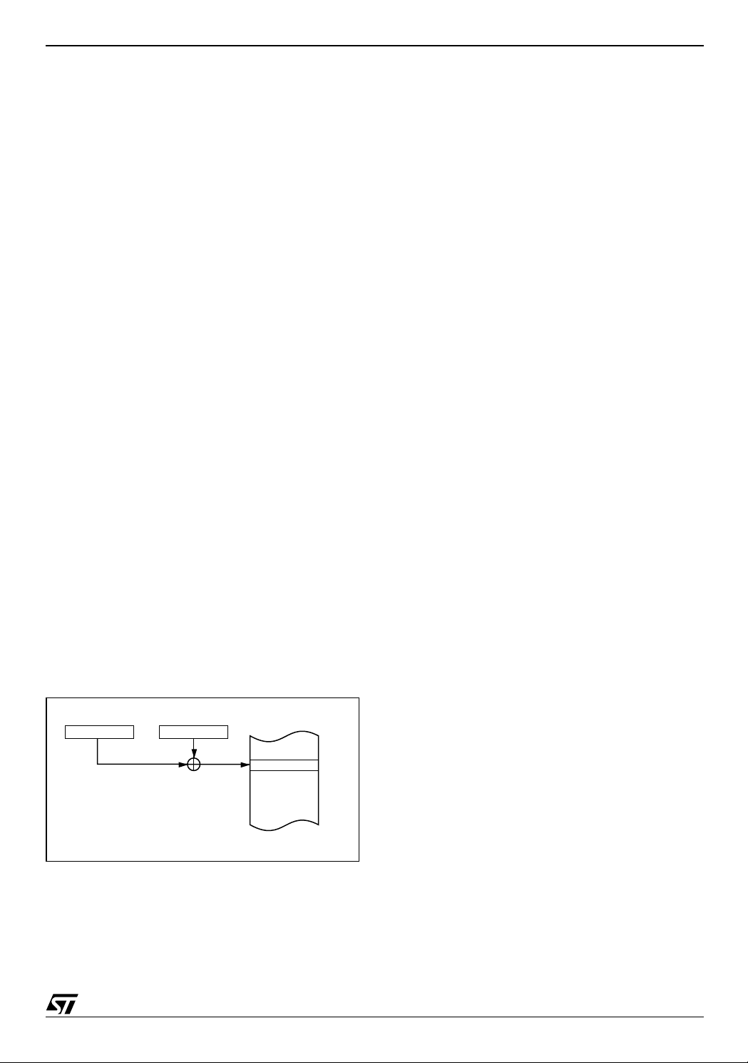
Serial Port Mode 0, Block Diagram (Figure 27.) . . . . . . . . . . . . . . . . . . . . . . . . . . . . . . . . . . . . . . . 59
Serial Port Control Register (SCON) (Table 43.). . . . . . . . . . . . . . . . . . . . . . . . . . . . . . . . . . . . . . . 59
Description of the SCON Bits (Table 44.) . . . . . . . . . . . . . . . . . . . . . . . . . . . . . . . . . . . . . . . . . . . .60
Timer 1-Generated Commonly Used Baud Rates (Table 45.) . . . . . . . . . . . . . . . . . . . . . . . . . . . . 62
Serial Port Mode 0, Waveforms (Figure 28.). . . . . . . . . . . . . . . . . . . . . . . . . . . . . . . . . . . . . . . . . .63
Serial Port Mode 1, Block Diagram (Figure 29.) . . . . . . . . . . . . . . . . . . . . . . . . . . . . . . . . . . . . . . . 64
Serial Port Mode 1, Waveforms (Figure 30.). . . . . . . . . . . . . . . . . . . . . . . . . . . . . . . . . . . . . . . . . .64
Serial Port Mode 2, Block Diagram (Figure 31.) . . . . . . . . . . . . . . . . . . . . . . . . . . . . . . . . . . . . . . . 66
Serial Port Mode 2, Waveforms (Figure 32.). . . . . . . . . . . . . . . . . . . . . . . . . . . . . . . . . . . . . . . . . .66
Serial Port Mode 3, Block Diagram (Figure 33.) . . . . . . . . . . . . . . . . . . . . . . . . . . . . . . . . . . . . . . . 67
Serial Port Mode 3, Waveforms (Figure 34.). . . . . . . . . . . . . . . . . . . . . . . . . . . . . . . . . . . . . . . . . .67
ANALOG-TO-DIGITAL CONVERTOR (ADC) . . . . . . . . . . . . . . . . . . . . . . . . . . . . . . . . . . . . . . . . . . . 68
ADC Interrupt. . . . . . . . . . . . . . . . . . . . . . . . . . . . . . . . . . . . . . . . . . . . . . . . . . . . . . . . . . . . . . . . . 68
A/D Block Diagram (Figure 35.). . . . . . . . . . . . . . . . . . . . . . . . . . . . . . . . . . . . . . . . . . . . . . . . . . . . 6 8
ADC SFR Memory Map (Table 46.) . . . . . . . . . . . . . . . . . . . . . . . . . . . . . . . . . . . . . . . . . . . . . . . . 69
Description of the ACON Bits (Table 47.) . . . . . . . . . . . . . . . . . . . . . . . . . . . . . . . . . . . . . . . . . . . .69
ADC Clock Input (Table 48.) . . . . . . . . . . . . . . . . . . . . . . . . . . . . . . . . . . . . . . . . . . . . . . . . . . . . . . 6 9
PULSE WIDTH MODULATION (PWM). . . . . . . . . . . . . . . . . . . . . . . . . . . . . . . . . . . . . . . . . . . . . . . . . 70
4-channel PWM Unit (PWM 0-3) . . . . . . . . . . . . . . . . . . . . . . . . . . . . . . . . . . . . . . . . . . . . . . . . . .70
Four-Channel 8-bit PWM Block Diagram (Figure 36.). . . . . . . . . . . . . . . . . . . . . . . . . . . . . . . . . . . 71
PWM SFR Memory Map (Table 49.). . . . . . . . . . . . . . . . . . . . . . . . . . . . . . . . . . . . . . . . . . . . . . . . 72
Programmable Period 8-bit PWM. . . . . . . . . . . . . . . . . . . . . . . . . . . . . . . . . . . . . . . . . . . . . . . . . 73
Programmable PWM 4 Channel Block Diagram (Figure 37.) . . . . . . . . . . . . . . . . . . . . . . . . . . . . . 73
PWM 4 Channel Operation . . . . . . . . . . . . . . . . . . . . . . . . . . . . . . . . . . . . . . . . . . . . . . . . . . . . . . 7 4
PWM 4 With Programmable Pulse Width and Frequency (Figure 38.) . . . . . . . . . . . . . . . . . . . . . . 74
5/152

UPSD3212C, UPSD3212CV
I2C INTERFACE . . . . . . . . . . . . . . . . . . . . . . . . . . . . . . . . . . . . . . . . . . . . . . . . . . . . . . . . . . . . . . . . . . 75
Block Diagram of the I2C Bus Serial I/O (Figure 39.) . . . . . . . . . . . . . . . . . . . . . . . . . . . . . . . . . . . 75
Serial Control Register (S2CON) (Table 50.) . . . . . . . . . . . . . . . . . . . . . . . . . . . . . . . . . . . . . . . . . 76
Description of the S2CON Bits (Table 51.) . . . . . . . . . . . . . . . . . . . . . . . . . . . . . . . . . . . . . . . . . . .76
Selection of the Serial Clock Frequency SCL in Master Mode (Table 52.) . . . . . . . . . . . . . . . . . . . 76
Serial Status Register (S2STA) . . . . . . . . . . . . . . . . . . . . . . . . . . . . . . . . . . . . . . . . . . . . . . . . . . 77
Data Shift Register (S2DAT). . . . . . . . . . . . . . . . . . . . . . . . . . . . . . . . . . . . . . . . . . . . . . . . . . . . . 77
Serial Status Register (S2STA) (Table 53.). . . . . . . . . . . . . . . . . . . . . . . . . . . . . . . . . . . . . . . . . . .77
Description of the S2STA Bits (Table 54.). . . . . . . . . . . . . . . . . . . . . . . . . . . . . . . . . . . . . . . . . . . .77
Data Shift Register (S2DAT) (Table 55.). . . . . . . . . . . . . . . . . . . . . . . . . . . . . . . . . . . . . . . . . . . . .77
Address Register (S2ADR) . . . . . . . . . . . . . . . . . . . . . . . . . . . . . . . . . . . . . . . . . . . . . . . . . . . . . . 7 8
Address Register (S2ADR) (Table 56.). . . . . . . . . . . . . . . . . . . . . . . . . . . . . . . . . . . . . . . . . . . . . . 78
Start /Stop Hold Time Detection Register (S2SETUP) (Table 57.). . . . . . . . . . . . . . . . . . . . . . . . .78
System Cock of 40MHz (Table 58.). . . . . . . . . . . . . . . . . . . . . . . . . . . . . . . . . . . . . . . . . . . . . . . . .78
System Clock Setup Examples (Table 59.). . . . . . . . . . . . . . . . . . . . . . . . . . . . . . . . . . . . . . . . . . . 78
PSD MODULE. . . . . . . . . . . . . . . . . . . . . . . . . . . . . . . . . . . . . . . . . . . . . . . . . . . . . . . . . . . . . . . . . . . . 79
Functional Overview . . . . . . . . . . . . . . . . . . . . . . . . . . . . . . . . . . . . . . . . . . . . . . . . . . . . . . . . . . . 79
PSD MODULE Block Diagram (Figure 40.) . . . . . . . . . . . . . . . . . . . . . . . . . . . . . . . . . . . . . . . . . . .80
In-System Programming (ISP) . . . . . . . . . . . . . . . . . . . . . . . . . . . . . . . . . . . . . . . . . . . . . . . . . . .81
Methods of Programming Different Functional Blocks of the PSD MODULE (Table 60.). . . . . . . . 81
DEVELOPMENT SYSTEM . . . . . . . . . . . . . . . . . . . . . . . . . . . . . . . . . . . . . . . . . . . . . . . . . . . . . . . . . . 82
PSDsoft Express Development Tool (Figure 41.) . . . . . . . . . . . . . . . . . . . . . . . . . . . . . . . . . . . . . . 82
PSD MODULE REGISTER DESCRIPTION AND ADDRESS OFFSET . . . . . . . . . . . . . . . . . . . . . . . . 83
Register Address Offset (Table 61.) . . . . . . . . . . . . . . . . . . . . . . . . . . . . . . . . . . . . . . . . . . . . . . . . 83
PSD MODULE DETAILED OPERATION . . . . . . . . . . . . . . . . . . . . . . . . . . . . . . . . . . . . . . . . . . . . . . . 84
MEMORY BLOCKS. . . . . . . . . . . . . . . . . . . . . . . . . . . . . . . . . . . . . . . . . . . . . . . . . . . . . . . . . . . . . . . . 84
Primary Flash Memory and Second ary Flash memo ry Descr ip tion . . . . . . . . . . . . . . . . . . . . . 84
Memory Block Select Signals. . . . . . . . . . . . . . . . . . . . . . . . . . . . . . . . . . . . . . . . . . . . . . . . . . . . 84
Instructions . . . . . . . . . . . . . . . . . . . . . . . . . . . . . . . . . . . . . . . . . . . . . . . . . . . . . . . . . . . . . . . . . . 85
Instructions (Table 62.) . . . . . . . . . . . . . . . . . . . . . . . . . . . . . . . . . . . . . . . . . . . . . . . . . . . . . . . . . .86
Power-down Instruction and Power-up Mode . . . . . . . . . . . . . . . . . . . . . . . . . . . . . . . . . . . . . . 87
READ . . . . . . . . . . . . . . . . . . . . . . . . . . . . . . . . . . . . . . . . . . . . . . . . . . . . . . . . . . . . . . . . . . . . . . . 8 7
Status Bit (Table 63.). . . . . . . . . . . . . . . . . . . . . . . . . . . . . . . . . . . . . . . . . . . . . . . . . . . . . . . . . . . . 88
Programming Flash Memory . . . . . . . . . . . . . . . . . . . . . . . . . . . . . . . . . . . . . . . . . . . . . . . . . . . .89
Data Polling Flowchart (Figure 42.). . . . . . . . . . . . . . . . . . . . . . . . . . . . . . . . . . . . . . . . . . . . . . . . . 8 9
Data Toggle Flowchart (Figure 43.). . . . . . . . . . . . . . . . . . . . . . . . . . . . . . . . . . . . . . . . . . . . . . . . . 90
6/152

UPSD3212C, UPSD3212CV
Erasing Flash Memory . . . . . . . . . . . . . . . . . . . . . . . . . . . . . . . . . . . . . . . . . . . . . . . . . . . . . . . . . 91
Specific Features. . . . . . . . . . . . . . . . . . . . . . . . . . . . . . . . . . . . . . . . . . . . . . . . . . . . . . . . . . . . . . 92
Sector Protection/Security Bit Definition – Flash Protection Register (Table 64.). . . . . . . . . . . . . .92
Sector Protection/Security Bit Definition – Secondary Flash Protection Register (Table 65.). . . . . 92
SRAM . . . . . . . . . . . . . . . . . . . . . . . . . . . . . . . . . . . . . . . . . . . . . . . . . . . . . . . . . . . . . . . . . . . . . . . 93
Sector Select and SRAM Select. . . . . . . . . . . . . . . . . . . . . . . . . . . . . . . . . . . . . . . . . . . . . . . . . .93
Priority Level of Memory and I/O Components in the PSD MODULE (Figure 44.) . . . . . . . . . . . . . 93
VM Register (Table 66.) . . . . . . . . . . . . . . . . . . . . . . . . . . . . . . . . . . . . . . . . . . . . . . . . . . . . . . . . . 94
Separate Space Mode (Figure 45.). . . . . . . . . . . . . . . . . . . . . . . . . . . . . . . . . . . . . . . . . . . . . . . . .95
Combined Space Mode (Figure 46.) . . . . . . . . . . . . . . . . . . . . . . . . . . . . . . . . . . . . . . . . . . . . . . . . 95
Page Register. . . . . . . . . . . . . . . . . . . . . . . . . . . . . . . . . . . . . . . . . . . . . . . . . . . . . . . . . . . . . . . . . 96
Page Register (Figure 47.) . . . . . . . . . . . . . . . . . . . . . . . . . . . . . . . . . . . . . . . . . . . . . . . . . . . . . . . 96
PLDs . . . . . . . . . . . . . . . . . . . . . . . . . . . . . . . . . . . . . . . . . . . . . . . . . . . . . . . . . . . . . . . . . . . . . . . . . . . 97
DPLD and CPLD Inputs (Table 67.) . . . . . . . . . . . . . . . . . . . . . . . . . . . . . . . . . . . . . . . . . . . . . . . .97
The Turbo Bit in PSD MODULE . . . . . . . . . . . . . . . . . . . . . . . . . . . . . . . . . . . . . . . . . . . . . . . . . .97
PLD Diagram (Figure 48.) . . . . . . . . . . . . . . . . . . . . . . . . . . . . . . . . . . . . . . . . . . . . . . . . . . . . . . . .98
Decode PLD (DPLD) . . . . . . . . . . . . . . . . . . . . . . . . . . . . . . . . . . . . . . . . . . . . . . . . . . . . . . . . . . . 99
DPLD Logic Array (Figure 49.) . . . . . . . . . . . . . . . . . . . . . . . . . . . . . . . . . . . . . . . . . . . . . . . . . . . . 99
Complex PLD (CPLD) . . . . . . . . . . . . . . . . . . . . . . . . . . . . . . . . . . . . . . . . . . . . . . . . . . . . . . . . . 10 0
Macrocell and I/O Port (Figure 50.). . . . . . . . . . . . . . . . . . . . . . . . . . . . . . . . . . . . . . . . . . . . . . . .100
Output Macrocell Port and Data Bit Assignments (Table 68.). . . . . . . . . . . . . . . . . . . . . . . . . . . . 101
Product Term Allocator. . . . . . . . . . . . . . . . . . . . . . . . . . . . . . . . . . . . . . . . . . . . . . . . . . . . . . . . 1 0 2
CPLD Output Macrocell (Figure 51.). . . . . . . . . . . . . . . . . . . . . . . . . . . . . . . . . . . . . . . . . . . . . . . 102
Input Macrocells (IMC) . . . . . . . . . . . . . . . . . . . . . . . . . . . . . . . . . . . . . . . . . . . . . . . . . . . . . . . . 103
Input Macrocell (Figure 52.). . . . . . . . . . . . . . . . . . . . . . . . . . . . . . . . . . . . . . . . . . . . . . . . . . . . . . 103
I/O PORTS (PSD MODULE) . . . . . . . . . . . . . . . . . . . . . . . . . . . . . . . . . . . . . . . . . . . . . . . . . . . . . . . . 104
General Port Architecture. . . . . . . . . . . . . . . . . . . . . . . . . . . . . . . . . . . . . . . . . . . . . . . . . . . . . . 1 0 4
General I/O Port Architecture (Figure 53.). . . . . . . . . . . . . . . . . . . . . . . . . . . . . . . . . . . . . . . . . . . 104
Port Operating Modes . . . . . . . . . . . . . . . . . . . . . . . . . . . . . . . . . . . . . . . . . . . . . . . . . . . . . . . . . 105
MCU I/O Mode . . . . . . . . . . . . . . . . . . . . . . . . . . . . . . . . . . . . . . . . . . . . . . . . . . . . . . . . . . . . . . . 105
PLD I/O Mode. . . . . . . . . . . . . . . . . . . . . . . . . . . . . . . . . . . . . . . . . . . . . . . . . . . . . . . . . . . . . . . . 105
Address Out Mod e . . . . . . . . . . . . . . . . . . . . . . . . . . . . . . . . . . . . . . . . . . . . . . . . . . . . . . . . . . . . 105
Peripheral I/O Mode. . . . . . . . . . . . . . . . . . . . . . . . . . . . . . . . . . . . . . . . . . . . . . . . . . . . . . . . . . . 105
7/152

UPSD3212C, UPSD3212CV
JTAG In-System Programming (ISP). . . . . . . . . . . . . . . . . . . . . . . . . . . . . . . . . . . . . . . . . . . . . 105
Peripheral I/O Mode (Figure 54.). . . . . . . . . . . . . . . . . . . . . . . . . . . . . . . . . . . . . . . . . . . . . . . . . . 106
Port Operating Modes (Table 69.). . . . . . . . . . . . . . . . . . . . . . . . . . . . . . . . . . . . . . . . . . . . . . . . .106
Port Operating Mode Settings (Table 70.). . . . . . . . . . . . . . . . . . . . . . . . . . . . . . . . . . . . . . . . . . . 106
I/O Port Latched Address Output Assignments (Table 71.) . . . . . . . . . . . . . . . . . . . . . . . . . . . . . 106
Port Configuration Registers (PCR) . . . . . . . . . . . . . . . . . . . . . . . . . . . . . . . . . . . . . . . . . . . . . 107
Port Configuration Registers (PCR) (Table 72.) . . . . . . . . . . . . . . . . . . . . . . . . . . . . . . . . . . . . . .107
Port Pin Direction Control, Output Enable P.T. Not Defined (Table 73.). . . . . . . . . . . . . . . . . . . . 107
Port Pin Direction Control, Output Enable P.T. Defined (Table 74.) . . . . . . . . . . . . . . . . . . . . . . . 107
Port Direction Assignment Example (Table 75.) . . . . . . . . . . . . . . . . . . . . . . . . . . . . . . . . . . . . . . 107
Port Data Registers. . . . . . . . . . . . . . . . . . . . . . . . . . . . . . . . . . . . . . . . . . . . . . . . . . . . . . . . . . . 108
Drive Register Pin Assignment (Table 76.) . . . . . . . . . . . . . . . . . . . . . . . . . . . . . . . . . . . . . . . . . . 108
Ports A and B – Functionality and Structure . . . . . . . . . . . . . . . . . . . . . . . . . . . . . . . . . . . . . . 109
Port A and Port B Structure (Figure 55.) . . . . . . . . . . . . . . . . . . . . . . . . . . . . . . . . . . . . . . . . . . . . 109
Port C – Functionality and Structure. . . . . . . . . . . . . . . . . . . . . . . . . . . . . . . . . . . . . . . . . . . . . 110
Port C Structure (Figure 56.). . . . . . . . . . . . . . . . . . . . . . . . . . . . . . . . . . . . . . . . . . . . . . . . . . . . . 110
Port D – Functionality and Structure. . . . . . . . . . . . . . . . . . . . . . . . . . . . . . . . . . . . . . . . . . . . . 111
Port D Structure (Figure 57.). . . . . . . . . . . . . . . . . . . . . . . . . . . . . . . . . . . . . . . . . . . . . . . . . . . . . 111
External Chip Select . . . . . . . . . . . . . . . . . . . . . . . . . . . . . . . . . . . . . . . . . . . . . . . . . . . . . . . . . .112
Port D External Chip Select Signals (Figure 58.) . . . . . . . . . . . . . . . . . . . . . . . . . . . . . . . . . . . . . 112
POWER MANAGEMENT . . . . . . . . . . . . . . . . . . . . . . . . . . . . . . . . . . . . . . . . . . . . . . . . . . . . . . . . . . 1 1 3
APD Unit (Figure 59.) . . . . . . . . . . . . . . . . . . . . . . . . . . . . . . . . . . . . . . . . . . . . . . . . . . . . . . . . . . 113
Enable Power-down Flow Chart (Figure 60.) . . . . . . . . . . . . . . . . . . . . . . . . . . . . . . . . . . . . . . . . 114
Power-down Mode’s Effect on Ports (Table 78.). . . . . . . . . . . . . . . . . . . . . . . . . . . . . . . . . . . . . . 114
PLD Power Management. . . . . . . . . . . . . . . . . . . . . . . . . . . . . . . . . . . . . . . . . . . . . . . . . . . . . . . 115
PSD Chip Select Input (CSI, PD2) . . . . . . . . . . . . . . . . . . . . . . . . . . . . . . . . . . . . . . . . . . . . . . . 115
Input Clock . . . . . . . . . . . . . . . . . . . . . . . . . . . . . . . . . . . . . . . . . . . . . . . . . . . . . . . . . . . . . . . . . . 1 1 5
Input Control Signals . . . . . . . . . . . . . . . . . . . . . . . . . . . . . . . . . . . . . . . . . . . . . . . . . . . . . . . . . 115
Power Management Mode Registers PMMR0 (Table 79.) . . . . . . . . . . . . . . . . . . . . . . . . . . . . . . 115
Power Management Mode Registers PMMR2 (Table 80.) . . . . . . . . . . . . . . . . . . . . . . . . . . . . . . 116
APD Counter Operation (Table 81.) . . . . . . . . . . . . . . . . . . . . . . . . . . . . . . . . . . . . . . . . . . . . . . . 116
RESET TIMING AND DEVICE STATUS AT RESET . . . . . . . . . . . . . . . . . . . . . . . . . . . . . . . . . . . . . 117
Warm RESET . . . . . . . . . . . . . . . . . . . . . . . . . . . . . . . . . . . . . . . . . . . . . . . . . . . . . . . . . . . . . . . . 117
I/O Pin, Register and PLD Status at RESET . . . . . . . . . . . . . . . . . . . . . . . . . . . . . . . . . . . . . . . 117
Reset (RESET) Timing (Figure 61.) . . . . . . . . . . . . . . . . . . . . . . . . . . . . . . . . . . . . . . . . . . . . . . . 117
Status During Power-on RESET, Warm RESET and Power-down Mode (Table 82.). . . . . . . . . .117
8/152

UPSD3212C, UPSD3212CV
PROGRAMMING IN-CIRCUIT USING THE JTAG SERIAL INTERFACE . . . . . . . . . . . . . . . . . . . . . 118
Standard JTAG Signals. . . . . . . . . . . . . . . . . . . . . . . . . . . . . . . . . . . . . . . . . . . . . . . . . . . . . . . . 118
JTAG Port Signals (Table 83.). . . . . . . . . . . . . . . . . . . . . . . . . . . . . . . . . . . . . . . . . . . . . . . . . . . . 118
JTAG Extensions . . . . . . . . . . . . . . . . . . . . . . . . . . . . . . . . . . . . . . . . . . . . . . . . . . . . . . . . . . . . . 118
Security and Flash memory Protection. . . . . . . . . . . . . . . . . . . . . . . . . . . . . . . . . . . . . . . . . . . 118
INITIAL DELIVERY STATE. . . . . . . . . . . . . . . . . . . . . . . . . . . . . . . . . . . . . . . . . . . . . . . . . . . . . . . . . 118
AC/DC PARAMETERS . . . . . . . . . . . . . . . . . . . . . . . . . . . . . . . . . . . . . . . . . . . . . . . . . . . . . . . . . . . . 119
PLD ICC /Frequency Consumption (5V range) (Figure 62.) . . . . . . . . . . . . . . . . . . . . . . . . . . . . . 119
PLD ICC /Frequency Consumption (3V range) (Figure 63.) . . . . . . . . . . . . . . . . . . . . . . . . . . . . . 119
PSD MODULE Example, Typ. Power Calculation at V
MAXIMUM RATING. . . . . . . . . . . . . . . . . . . . . . . . . . . . . . . . . . . . . . . . . . . . . . . . . . . . . . . . . . . . . . . 121
Absolute Maximum Ratings (Table 85.) . . . . . . . . . . . . . . . . . . . . . . . . . . . . . . . . . . . . . . . . . . . . 121
DC AND AC PARAMETERS. . . . . . . . . . . . . . . . . . . . . . . . . . . . . . . . . . . . . . . . . . . . . . . . . . . . . . . . 122
Operating Conditions (5V Devices) (Table 86.). . . . . . . . . . . . . . . . . . . . . . . . . . . . . . . . . . . . . . . 122
Operating Conditions (3V Devices) (Table 87.). . . . . . . . . . . . . . . . . . . . . . . . . . . . . . . . . . . . . . . 122
AC Symbols for Timing (Table 88.) . . . . . . . . . . . . . . . . . . . . . . . . . . . . . . . . . . . . . . . . . . . . . . . . 123
Switching Waveforms – Key (Figure 64.) . . . . . . . . . . . . . . . . . . . . . . . . . . . . . . . . . . . . . . . . . . . 123
DC Characteristics (5V Devices) (Table 89.). . . . . . . . . . . . . . . . . . . . . . . . . . . . . . . . . . . . . . . . . 124
DC Characteristics (3V Devices) (Table 90.). . . . . . . . . . . . . . . . . . . . . . . . . . . . . . . . . . . . . . . . . 126
External Program Memory READ Cycle (Figure 65.) . . . . . . . . . . . . . . . . . . . . . . . . . . . . . . . . . . 128
External Program Memory AC Characteristics (with the 5V MCU Module) (Table 91.) . . . . . . . . 128
External Program Memory AC Characteristics (with the 3V MCU Module) (Table 92.) . . . . . . . . 129
External Clock Drive (with the 5V MCU Module) (Table 93.) . . . . . . . . . . . . . . . . . . . . . . . . . . . .129
External Clock Drive (with the 3V MCU Module) (Table 94.) . . . . . . . . . . . . . . . . . . . . . . . . . . . .129
External Data Memory READ Cycle (Figure 66.) . . . . . . . . . . . . . . . . . . . . . . . . . . . . . . . . . . . . . 130
External Data Memory WRITE Cycle (Figure 67.). . . . . . . . . . . . . . . . . . . . . . . . . . . . . . . . . . . . . 130
External Data Memory AC Characteristics (with the 5V MCU Module) (Table 95.). . . . . . . . . . . . 131
External Data Memory AC Characteristics (with the 3V MCU Module) (Table 96.). . . . . . . . . . . . 132
A/D Analog Specification (Table 97.). . . . . . . . . . . . . . . . . . . . . . . . . . . . . . . . . . . . . . . . . . . . . . . 132
Input to Output Disable / Enable (Figure 68.) . . . . . . . . . . . . . . . . . . . . . . . . . . . . . . . . . . . . . . . . 133
CPLD Combinatorial Timing (5V Devices) (Table 98.) . . . . . . . . . . . . . . . . . . . . . . . . . . . . . . . . . 133
CPLD Combinatorial Timing (3V Devices) (Table 99.) . . . . . . . . . . . . . . . . . . . . . . . . . . . . . . . . . 133
Synchronous Clock Mode Timing – PLD (Figure 69.). . . . . . . . . . . . . . . . . . . . . . . . . . . . . . . . . . 134
CPLD Macrocell Synchronous Clock Mode Timing (5V Devices) (Table 100.). . . . . . . . . . . . . . . 134
CPLD Macrocell Synchronous Clock Mode Timing (3V Devices) (Table 101.). . . . . . . . . . . . . . . 135
Asynchronous RESET / Preset (Figure 70.) . . . . . . . . . . . . . . . . . . . . . . . . . . . . . . . . . . . . . . . . . 136
Asynchronous Clock Mode Timing (product term clock) (Figure 71.) . . . . . . . . . . . . . . . . . . . . . . 136
CPLD Macrocell Asynchronous Clock Mode Timin g (5V Devices) (Table 102.). . . . . . . . . . . . . . 136
CPLD Macrocell Asynchronous Clock Mode Timin g (3V Devices) (Table 103.). . . . . . . . . . . . . . 137
= 5.0V (Turbo Mode Off) (Table 84.). . 120
CC
9/152

UPSD3212C, UPSD3212CV
Input Macrocell Timing (product term clock) (Figure 72.) . . . . . . . . . . . . . . . . . . . . . . . . . . . . . . . 138
Input Macrocell Timing (5V Devices) (Table 104.) . . . . . . . . . . . . . . . . . . . . . . . . . . . . . . . . . . . . 138
Input Macrocell Timing (3V Devices) (Table 105.) . . . . . . . . . . . . . . . . . . . . . . . . . . . . . . . . . . . . 138
Program, WRITE and Erase Times (5V Devices) (Table 106.). . . . . . . . . . . . . . . . . . . . . . . . . . . 139
Program, WRITE and Erase Times (3V Devices) (Table 107.). . . . . . . . . . . . . . . . . . . . . . . . . . . 139
Peripheral I/O READ Timing (Figure 73.) . . . . . . . . . . . . . . . . . . . . . . . . . . . . . . . . . . . . . . . . . . . 140
Port A Peripheral Data Mode READ Timing (5V Devices) (Table 108.) . . . . . . . . . . . . . . . . . . . . 140
Port A Peripheral Data Mode READ Timing (3V Devices) (Table 109.) . . . . . . . . . . . . . . . . . . . . 140
Peripheral I/O WRITE Timing (Figure 74.) . . . . . . . . . . . . . . . . . . . . . . . . . . . . . . . . . . . . . . . . . . 141
Port A Peripheral Data Mode WRITE Timing (5V Devices) (Table 110.) . . . . . . . . . . . . . . . . . . . 141
Port A Peripheral Data Mode WRITE Timing (3V Devices) (Table 111.) . . . . . . . . . . . . . . . . . . . 141
Reset (RESET) Timing (5V Devices) (Table 112.) . . . . . . . . . . . . . . . . . . . . . . . . . . . . . . . . . . . . 142
Reset (RESET) Timing (3V Devices) (Table 113.) . . . . . . . . . . . . . . . . . . . . . . . . . . . . . . . . . . . . 142
V
STBYON
V
STBYON
ISC Timing (Figure 76.). . . . . . . . . . . . . . . . . . . . . . . . . . . . . . . . . . . . . . . . . . . . . . . . . . . . . . . . . 143
ISC Timing (5V Devices) (Table 116.) . . . . . . . . . . . . . . . . . . . . . . . . . . . . . . . . . . . . . . . . . . . . . . 143
ISC Timing (3V Devices) (Table 117.) . . . . . . . . . . . . . . . . . . . . . . . . . . . . . . . . . . . . . . . . . . . . . . 144
MCU Module AC Measurement I/O Waveform (Figure 77.) . . . . . . . . . . . . . . . . . . . . . . . . . . . . . 144
PSD MODULE AC Float I/O Waveform (Figure 78.). . . . . . . . . . . . . . . . . . . . . . . . . . . . . . . . . . . 144
External Clock Cycle (Figure 79.) . . . . . . . . . . . . . . . . . . . . . . . . . . . . . . . . . . . . . . . . . . . . . . . . . 145
Recommended Oscillator Circuits (Figure 80.) . . . . . . . . . . . . . . . . . . . . . . . . . . . . . . . . . . . . . . . 145
PSD MODULE AC Measurement I/O Waveform (Figure 81.). . . . . . . . . . . . . . . . . . . . . . . . . . . . 145
PSD MODULEAC Measurem ent Load Circuit (Figure 82.). . . . . . . . . . . . . . . . . . . . . . . . . . . . . . 145
Capacitance (Table 118.) . . . . . . . . . . . . . . . . . . . . . . . . . . . . . . . . . . . . . . . . . . . . . . . . . . . . . . . 1 4 5
Definitions Timing (5V Devices) (Table 114.). . . . . . . . . . . . . . . . . . . . . . . . . . . . . . . . . 142
Timing (3V Devices) (Table 115.). . . . . . . . . . . . . . . . . . . . . . . . . . . . . . . . . . . . . . . . . . 142
PACKAGE MECHANICAL INFORMATION . . . . . . . . . . . . . . . . . . . . . . . . . . . . . . . . . . . . . . . . . . . . 146
PART NUMBERING . . . . . . . . . . . . . . . . . . . . . . . . . . . . . . . . . . . . . . . . . . . . . . . . . . . . . . . . . . . . . . 150
10/152

SUMMARY DESCRIPTION
■ Dual bank Flash memories
– Concurrent operation, read from memory
while erasing and writing the other. In-Application Programming (IAP) for remote updates
– Large 64KByte main Flash memory for appli-
cation code, operating systems, or bit maps
for graphic user interfaces
– Large 16KByte secondary Flash m emory di-
vided in small sectors. Eliminate external EEPROM with software EEPROM emulation
– Secondary Flash memory is large enough for
sophisticated communicat ion protoc ol du ring
IAP while continuing critical system tasks
■ Large SRAM with battery back-up option
– 2KByte SRAM for RTOS, high-level languag-
es, communication buffers, and stacks
■ Programmable Decode PLD for flexible address
mapping of all memories
– Place individual Flash an d SRAM sectors on
any address boundary
– Built-in page regist er breaks restrictive 8032
limit of 64KByte address space
– Special register swaps Flash memory seg-
ments between 8032 “program” space and
“data” space for efficient In-Application Programming
■ High-speed clock standard 8032 core (12-cycle)
– 40MHz operation at 5V, 24MHz at 3.3V
– 2 UARTs with independent baud rat e, three
16-bit Timer/Counters and two External Interrupts
2
■ I
C interface for peripheral connections
– Capable of master or slave operation
■ 5 Pulse Width Modulator (PWM) channels
– Four 8-bi t PWM un its
– One 8-bit PWM unit with prog ramm abl e peri-
od
UPSD3212C, UPSD3212CV
■ 4-channel, 8-bit Analog-to-Digital Converter
(ADC) with analog supply voltage (V
■ Six I/O ports with up to 46 I/O pins
2
– Multifunction I/O: GPI O, I
C, PWM, PLD I/O,
supervisor, and JTAG
– Eliminates need for external latches and logic
■ 3000 gate PLD with 16 macrocells
– Create glue logic, state machines, delays,
etc.
– Eliminate external PALs, PLDs, and 74HCxx
– Simple PSDsoft Express software... Free
■ Supervisor functions
– Generates reset upon low voltage or watch-
dog time-out. Eliminate external supervisor
device
– RESET
■ In-System Programming (ISP) via JTAG
Input pin; Reset output via PLD
– Program entire chip in 10 - 25 seconds with
no involvement of 8032
– Allows efficient manu facturing, easy product
testing, and Just-In-Time inventory
– Eliminate sockets and pre-programmed parts
TM
– Program with FlashLINK
■ Content Security
cable and any PC
– Programmable Security Bit blocks access of
device programmers and readers
■ Zero-Power Technology
– Memories and PLD automatically reach
standby current between input changes
■ Packages
– 52-pin TQFP
– 80-pin TQFP: allows access to 8032 address/
data/control signals for connecting to external
peripherals
REF
)
11/152
UPSD3212C, UPSD3212CV
Table 1. uPSD321X Devices Product Matrix
Main
Part No.
Flash
uPSD3212C-40T6 512K 128K 16K 16 37 5 3 2 1 4 5V 40 52
uPSD3212CV-24T6 512K 128K 16K 16 37 5 3 2 1 4 3V 24 52
uPSD3212C-40U6 512K 128K 16K 16 46 5 3 2 1 4 5V 40 80
uPSD3212CV-24U6 512K 128K 16K 16 46 5 3 2 1 4 3V 24 80
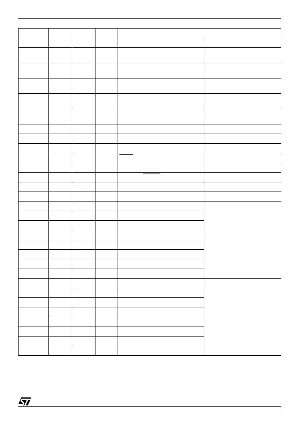
Figure 3. TQ FP 52 Connection s
(bit)
Sec.
Flash
SRAM
(bit)
PB0
52515049484746454443424140
(bit)
PB1
PB2
Macro
-Cells
PB3
PB4
Pins
PB5
I/O
VREF
GND
PWM
Ch.
RESET
PB6
Timer
/ Ctr
PB7
P1.7/ADC3
UART
Ch.
P1.6/ADC2
ADC
2
C
I
Ch.
V
CC
MHz Pins
PD1
1
PC7
2
PC6
3
PC5
4
See note
Note: 1. Pull-up resis tor requ i r ed on pin 5 (2kΩ for 3V devices, 7.5kΩ for 5V dev i ces).
2. NC = Not Connected.
(1)
PC4
NC
V
CC
GND
PC3
PC2
PC1
PC0
5
6
7
8
9
10
11
12
13
14151617181920212223242526
GND
P4.2
P4.1
P4.0
P3.1 / TXD
P4.7 / PWM4
P4.6 / PWM3
P4.5 / PWM2
P4.4 / PWM1
P4.3 / PWM0
P3.0 / RXD
P3.2 / EXINT0
P3.3 / EXINT1
39 P1.5 / ADC1
38 P1.4 / ADC0
37 P1.3 / TXD1
36 P1.2 / RXD1
35 P1.1 / T2X
34 P1.0 / T2
33 V
CC
32 XTAL2
31 XTAL1
30 P3.7 / SCL1
29 P3.6 / SDA1
28 P3.5 / T1
27 P3.4 / T0
AI07423
12/152

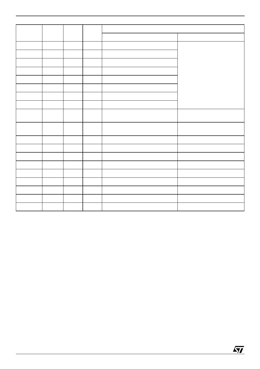
Figure 4. TQ FP 80 Connection s
PB0
P3.2 / EXINT0
80797877767574737271706968676665646362
PB1
P3.1 / TXD
PB2
P3.0 / RXD
PB3
PB4
PB5NCVREF
GND
RESET
PB6
UPSD3212C, UPSD3212CV
PB7
RD, CNTL1
P1.7 / ADC3
PSEN, CNTL2
WR, CNTL0
P1.6 / ADC2
61
PD2
P3.3 /EXINT1
PD1
PD0, ALE
PC7
PC6
PC5
See note
P4.7 / PWM4
P4.6 / PWM3
(1)
PC4
NC
NC
V
CC
GND
PC3
PC2
PC1
NC
PC0
1
2
3
4
5
6
7
8
9
10
11
12
13
14
15
16
17
18
19
20
21222324252627282930313233343536373839
40
60 P1.5 / ADC1
59 P1.4 / ADC0
58 P1.3 / TXD1
57 P2.3, A11
56 P1.2 / RXD1
55 P2.2, A10
54 P1.1 / T2X
53 P2.1, A9
52 P1.0 / T2
51 P2.0, A8
50 V
CC
49 XTAL2
48 XTAL1
47 P0.7, AD7
46 P3.7 / SCL1
45 P0.6, AD6
44 P3.6 / SDA1
43 P0.5, AD5
42 P3.5 / T1
41 P0.4, AD4
PA7
PA6
PA5
PA4
PA3
GND
P4.5 / PWM2
P4.4 / PWM1
P4.3 / PWM0
Note: 1. Pull-up resis tor requ i r ed on pin 8 (2kΩ for 3V devices, 7.5kΩ for 5V dev i ces).
2. NC = Not Connected.
P4.2
P4.1
PA2
P4.0
PA1
PA0
AD0, P0.0
AD1, P0.1
AD2, P0.2
AD3, P0.3
P3.4 / T0
AI07424
13/152

UPSD3212C, UPSD3212CV
Table 2. 80-Pin Package Pin Description
Port Pin
P0.0 AD0 36 I/O
P0.1 AD1 37 I/O Multiplexed Address/Data bus A0/D0
P0.2 AD2 38 I/O Multiplexed Address/Data bus A2/D2
P0.3 AD3 39 I/O Multiplexed Address/Data bus A3/D3
P0.4 AD4 41 I/O Multiplexed Address/Data bus A4/D4
P0.5 AD5 43 I/O Multiplexed Address/Data bus A5/D5
P0.6 AD6 45 I/O Multiplexed Address/Data bus A6/D6
P0.7 AD7 47 I/O Multiplexed Address/Data bus A7/D7
P1.0 T2 52 I/O General I/O port pin Timer 2 Count input
P1.1 T2EX 54 I/O General I/O port pin Timer 2 Trigger input
P1.2 RxD2 56 I/O General I/O port pin 2nd UART Receive
P1.3 TxD2 58 I/O General I/O port pin 2nd UART Transmit
P1.4 ADC0 59 I/O General I/O port pin ADC Channel 0 input
P1.5 ADC1 60 I/O General I/O port pin ADC Channel 1 input
P1.6 ADC2 61 I/O General I/O port pin ADC Channel 2 input
P1.7 ADC3 64 I/O General I/O port pin ADC Channel 3 input
Signal
Name
Pin No. In/Out
Basic Alternate
External Bus
Multiplexed Address/Data bus A1/D1
Function
P2.0 A8 51 O External Bus, Address A8
P2.1 A9 53 O External Bus, Address A9
P2.2 A10 55 O External Bus, Address A10
P2.3 A11 57 O External Bus, Address A11
P3.0 RxD1 75 I/O General I/O port pin UART Receive
P3.1 TxD1 77 I/O General I/O port pin UART Transmit
P3.2 INTO 79 I/O General I/O port pin
P3.3 INT1 2 I/O General I/O port pin
P3.4 T0 40 I/O General I/O port pin Counter 0 input
P3.5 T1 42 I/O General I/O port pin Counter 1 input
P3.6 SDA1 44 I/O General I/O port pin
P3.7 SCL1 46 I/O General I/O port pin
P4.0 33 I/O General I/O port pin
P4.1 31 I/O General I/O port pin
P4.2 30 I/O General I/O port pin
P4.3 PWM0 27 I/O General I/O port pin
Interrupt 0 input / Timer 0 gate
control
Interrupt 1 input / Timer 1 gate
control
2
I
C Bus serial data I/O
2
I
C Bus clock I/O
8-bit Pulse Width Modulation
output 0
14/152
UPSD3212C, UPSD3212CV
Port Pin
P4.4 PWM1 25 I/O General I/O port pin
P4.5 PWM2 23 I/O General I/O port pin
P4.6 PWM3 19 I/O General I/O port pin
P4.7 PWM4 18 I/O General I/O port pin
Signal
Name
PUP 8 I/O
AVREF 70 O Reference Voltage input for ADC
RD_ 65 O READ signal, external bus
WR_ 62 O WRITE signal, external bus
PSEN_ 63 O PSEN
ALE 4 O Address Latch signal, external bus
RESET_ 68 I Active low RESET
XTAL1 48 I Oscillator input pin for system clock
XTAL2 49 O Oscillator output pin for system clock
Pin No. In/Out
Pull-up resistor required (2kΩ for 3V
devices, 7.5kΩ for 5V devices)
signal, external bus
Function
Basic Alternate
8-bit Pulse Width Modulation
output 1
8-bit Pulse Width Modulation
output 2
8-bit Pulse Width Modulation
output 3
Programmable 8-bit Pulse Width
modulation output 4
input
PA0 35 I/O General I/O port pin
PA1 34 I/O General I/O port pin
PA2 32 I/O General I/O port pin
PA3 28 I/O General I/O port pin
PA4 26 I/O General I/O port pin
PA5 24 I/O General I/O port pin
PA6 22 I/O General I/O port pin
PA7 21 I/O General I/O port pin
PB0 80 I/O General I/O port pin
PB1 78 I/O General I/O port pin
PB2 76 I/O General I/O port pin
PB3 74 I/O General I/O port pin
PB4 73 I/O General I/O port pin
PB5 72 I/O General I/O port pin
PB6 67 I/O General I/O port pin
PB7 66 I/O General I/O port pin
1. PLD Macro-cell outputs
2. PLD inputs
3. Latched Address Out (A0-A7)
4. Peripheral I/O Mode
1. PLD Macro-cell outputs
2. PLD inputs
3. Latched Address Out (A0-A7)
15/152
UPSD3212C, UPSD3212CV
Port Pin
PC0 TMS 20 I JTAG pin
PC1 TCK 16 I JTAG pin
PC2
PC3 TSTAT 14 I/O General I/O port pin
PC4 TERR 9 I/O General I/O port pin
PC5 TDI 7 I JTAG pin
PC6 TDO 6 O JTAG pin
PC7 5 I/O General I/O port pin
PD1 CLKIN 3 I/O General I/O port pin
PD2 CSI 1 I/O General I/O port pin
Vcc 12
Vcc 50
GND 13
GND 29
GND 69
NC 10
Signal
Name
V
STBY
Pin No. In/Out
15 I/O General I/O port pin
Function
Basic Alternate
1. PLD Macro-cell outputs
2. PLD inputs
3. SRA M stand by voltage input
4. SRAM battery-on indicator
5. JTAG pins are dedicated pins
1. PLD I/O
2. Clock input to PLD and APD
1. PLD I/O
2. Chip select to PSD Module
(V
STBY
(PC4)
)
NC 11
NC 17
NC 71
52 PIN PACKAGE I/O PORT
The 52-pin package members of the uPSD321X
Devices have the same port pins as those of the
80-pin package except:
■ Port 0 (P0.0-P0.7, external address/data bus
AD0-AD7)
■ Port 2 (P2.0-P2.3, external address bus A8-
A11)
■ Port A (PA0-PA7)
■ Port D (PD2)
■ Bus control signal (RD,WR,PSEN,ALE)
Pin 5 requires a pull-up resistor (2kΩ for 3V devices, 7.5kΩ for 5V devices) for all devices.
16/152
ARCHITECTURE OVERVIEW
Memory Organization
The uPSD321X Devices’s standard 8032 Core
has separate 64KB address spac es for Program
memory and Data Memory. Program memory is
where the 8032 executes in structions from. Data
memory is used to hold data variables. Flash
memory can be mapped in either program or data
space. The Flash memory consists of two flash
memory blocks: the main Flash (512Kbit) and the
Secondary Flash (128Kbit). Except during flash
memory programming or update, Flash memory
can only be read, not written to. A Page Register
is used to access memory beyond t he 64K bytes
Figure 5. Memory Map and Address Space
MAIN
FLASH
UPSD3212C, UPSD3212CV
address space. Refer to the PSD Module for details on mapping of the Flash memory.
The 8032 core h as t wo ty pes of data m em ory (internal and external) that can be read and written.
The internal SRAM cons ists of 256 byte s, and includes the stack area.
The SFR (Special Function Registers) occupies
the upper 128 bytes of the internal SRAM, the registers can be accessed by Direct addressing only.
Another 2K bytes resides in the PSD Modul e that
can be mapped to any address space defined by
the user.
EXT. RAM
SECONDARY
FLASH
16KB
Flash Memory Space
64KB
INT. RAM
FF
Indirect
Addressing
7F
Indirect
Direct
Addressing
0
Internal RAM Space
(256 Bytes)
SFR
Direct
Addressing
or
2KB
External RAM Space
(MOVX)
AI07425
17/152
UPSD3212C, UPSD3212CV
Registers
The 8032 has several registers; these are the Program Counter (PC), Accumulator (A), B Register
(B), the Stack Pointer (SP), the Program Status
Word (PSW), General purpose registers (R0 to
R7), and DPTR (Data Pointer register).
Accumulator. The Ac cumulator is the 8-bit general purpose register, used for data operation such
as transfer, temporary saving, and conditional
tests. The Accumulator can be used as a 16-bit
register with B Register as shown in Figure 6.
B Register. The B Register is the 8-bit general
purpose register, used f or an arithmetic operation
such as multiply, division with the Accumulator
(see Figure 7).
Stack Pointer. The Stack Pointer Register is 8
bits wide. It is incremented before data is stored
during PUSH and CALL executions. While the
stack may reside anywhere in on-chip RAM, the
Stack Po inter is initi alize d to 07h af ter reset. Th is
causes the stack to begin at location 08h (see Figure 8).
Program Counter. The Program Counter is a 16bit wide which consists of two 8-bit registers, PCH
and PCL. This counter indicates the address of the
next instruction to be executed. In RESET
the program counter has reset routine address
(PCH:00h, PCL:00h).
Program Status Word. The Program Status
Word (PSW) contains several bits that reflect the
current state of the CPU and select Internal RAM
(00h to 1Fh: Bank0 to Bank3). The PSW is described in Figure 9, page 19. It contains the Carry
Flag, the Auxiliary Carry Flag, the Half Carry (for
BCD operation), the general purpose flag, the
Register Bank Select Flags, the Overflow Flag,
and Parity Flag.
[Carry Flag, CY]. This flag stores any carry or not
borrow from the ALU of CPU after an arithmetic
operation and is also changed by the Shift Instruction or Rotate Instruction.
[Auxiliary Carry Flag, AC]. After operation, this is
set when there is a carry from Bit 3 of ALU or there
is no borrow from Bit 4 of ALU.
[Register Bank Select Flags, RS0, RS1]. This flags
select one of four bank(00~07H:bank0,
08~0Fh:bank1, 10~17h: bank2, 17~1Fh:bank3) in
Internal RAM.
[Overflow Flag, OV]. This flag is set to '1' when an
overflow occurs as the result of an arithmetic operation involving signs. An overflow occurs when the
result of an addition or subtraction exceeds +127
(7Fh) or -128 (80h). The CLRV instruction clears
the overflow flag. There is no set instruction. When
state,
the BIT instruction is executed, Bit 6 of memory is
copied to this flag.
[Parity Flag, P]. This flag reflects on number of Accumulator’s “1.” If the number of Accumulator’s 1
is odd, P=0. otherwise, P=1. The sum of adding
Accumulator’s 1 to P is always even.
R0~R7. General purpose 8-bit registers that are
locked in the lower portion of internal data area.
Data Pointer Register. Data Pointer Register is
16-bit wide which consists of two-8bit registers,
DPH and DPL. This register is used as a data
pointer for the data transmission with external data
memory in the PSD Module.
Figure 6. 8032 MCU Registers
Accumulator
B Register
Stack Pointer
Program Counter
Program Status Word
General Purpose
Register (Bank0-3)
Data Pointer Register
AI06636
PCH
DPTR(DPH)
A
B
SP
PCL
PSW
R0-R7
DPTR(DPL)
Figure 7. Configuration of BA 16-bit Registers
B
AB
A
Two 8-bit Registers can be used as a "BA" 16-bit Registers
AI06637
Figure 8. Stack Pointer
Stack Area (30h-FFh)
Bit 15 Bit 0Bit 8 Bit 7
Hardware Fixed
SP (Stack Pointer) could be in 00h-FFh
SP00h
00h-FFh
AI06638
18/152
Figure 9. PSW (Program Status Word) Registe r
UPSD3212C, UPSD3212CV
MSB
CY
PSW
Carry Flag
Auxillary Carry Flag
General Purpose Flag
AC FO RS1 RS0 OV P
Register Bank Select Flags
(to select Bank0-3)
Program Memory
The program memory consists of two Flash memory: 64KByte Main Flash and 16KByte of Secondary Flash. The Flash mem ory can be mapped to
any address space as define d by the user in the
PSDsoft Tool. It can also be mapped to Data
memory space during Flash memory update or
programming.
After reset, the CPU begins execution from location 0000h. As shown in Figure 10, each interrupt
is assigned a fixed location in Program Memory.
The interrupt causes the CPU to jump to t hat location, where it commences execution of the service
routine. External Interrupt 0, for example, is assigned to location 0003h. If External Interrupt 0 is
going to be used, its service routine must begin at
location 0003h. If the interrupt is not going to be
used, its service location is available as gen eral
purpose Program Memory.
The interrupt service locations are spaced at 8byte intervals: 0003h for External Interrupt 0,
000Bh for Timer 0, 0013 h for E xternal I nterrupt 1,
001Bh for Timer 1 and so forth. If an interrupt service routine is short enough (as is often the c ase
in control applications), it can reside entirely within
that 8-byte interval (see Figure 10). Longer service
routines can use a jump instruction to s kip over
subsequent interrupt locat ions, if other interrupts
are in use.
Data memory
The internal data memory is divided into four physically separate d blocks: 256 bytes of internal RAM,
128 bytes of Special Function Registers (SFRs)
areas and 2K bytes (XRAM-PSD) in the PSD Module.
LSB
Reset Value 00h
Parity Flag
Bit not assigned
Overflow Flag
AI06639
RAM
Four register banks, each 8 registers wide, occupy
locations 0 through 31 in the lower RAM area.
Only one of these banks may be enabled at a time.
The next 16 bytes, locations 32 through 47, contain 128 directly addressable bit locations. The
stack depth is only limited by the available internal
RAM space of 256 bytes.
XRAM-PSD
The 2K bytes of XRAM-P SD resides in the PSD
Module and can be mapped to any address space
through the DPLD (Decoding PLD) as defined by
the user in PSDsoft Development tool. The XRAMPSD has a battery backup feature that allow the
data to be retained in t he event of a power lost.
The battery is connected t o the Port C PC2 pin.
This pin must be configured in PSDSoft to be battery back-up.
Figure 10. Inte rru pt Lo c atio n of P rog ra m Memory
008Bh
•
•
•
•
0013h
000Bh
0003h
0000hReset
8 Bytes
AI06640
Interrupt
Location
•
•
•
•
•
19/152
UPSD3212C, UPSD3212CV
SFR
The SFRs can only be addressed directly in the
address range from 80h to FFh. Table 15, page 32
gives an overview of the Speci al Function Registers. Sixteen address in the SFRs space are bothbyte and bit-addressable. The bit-addressable
SFRs are those whose address ends in 0h and 8h.
The bit addresses in this area are 80h to FFh.
Table 3. RAM Address
Byte Address
(in Hexadecimal)
↓↓
FFh 255
30h 48
Byte Address
(in Decimal)
Addressing Modes
The addressing modes in uPSD321 X Devices instruction set are as follows
■ Direct addressing
■ Indirect addressing
■ Register addressing
■ Register-specific addressing
■ Immediate constants addressing
■ Indexed addressing
(1) Direct addressing. I n a direct addressing t he
operand is specified by an 8-bit address field in the
instruction. Only internal Data RAM and SFRs
(80~FFH RAM) can be directly addressed.
Example:
msb Bit Address (Hex) lsb
2Fh 7F 7E 7D 7C 7B 7A 79 78 47
2Eh 77 76 75 74 73 72 71 70 46
2Dh 6F 6E 6D 6C 6B 6A 69 68 45
2Ch 67 66 65 64 63 62 61 60 44
2Bh 5F 5E 5D 5C 5B 5A 59 58 43
mov A, 3EH ;A <----- RAM[3E]
Figure 11. Direct Addressing
Program Memory
3Eh
04
A
2Ah 57 56 55 54 53 52 51 50 42
29h 4F 4E 4D 4C 4B 4A 49 48 41
28h 47 46 45 44 43 42 41 40 40
27h 3F 3E 3D 3C 3B 3A 39 38 39
26h 37 36 35 34 33 32 31 30 38
25h 2F 2E 2D 2C 2B 2A 29 28 37
24h 27 26 25 24 23 22 21 20 36
23h 1F 1E 1D 1C 1B 1A 19 18 35
22h 17 16 15 14 13 12 11 10 34
21h 0F 0E 0D 0C 0B 0A 09 08 33
20h 07 06 05 04 03 02 01 00 32
1Fh
Register Bank 3
18h 24
17h
Register Bank 2
10h 16
0Fh
Register Bank 1
08h 8
07h
Register Bank 0
00h 0
31
23
15
AI06641
(2) Indirect addressing. In indirect addressing
the instruction specifies a register which contains
the address of the operand. Both internal and external RAM can be indirectly addressed. The address register for 8-bit addresses can be R0 or R1
of the selected register bank, or the Stack Pointer.
The address register for 16-bit addresses can only
be the 16-bit “data pointer” register, DPTR.
Example:
mov @R1, #40 H ;[R1] <-----40H
Figure 12. Indirect Addressing
Program Memory
55h
7
R1
40h
55
AI06642
20/152
UPSD3212C, UPSD3212CV
(3) Register addressing. The register banks,
containing registers R0 through R7, can be accessed by certain instructions which carry a 3-bit
register specification within the opc ode of the instruction. Instructions that access the registers
this way are code efficient, since t his mode eliminates an address byte. When the instruction is executed, one of four banks is selected at execution
time by the two bank select bits in the PSW.
Example:
mov PSW, #0001000B ; select Bank0
mov A, #30H
mov R1, A
(4) Register-specific addressing. Some instructions are specific to a certain register. For example, some instructions always operate on the
Accumulator, or Data Pointer, etc., so no address
byte is needed to point it. The opcode it self does
that.
(5) Immediate constants addressing. The value of a constant can follow the opcode in Program
memory.
Example:
mov A, #10H.
(6) Indexed addressing. Only Program memory
can be accessed with indexed addressing, a nd it
can only be read. This addressing mode is intended for reading look-up tables in Program memory.
A 16-bit base register (either DPTR or PC) points
to the base of the table, and the Accumulator is set
up with the table entry number. The address of the
table entry in Program memory is formed by adding the Accumulator data to the bas e p ointer (see
Figure 13).
Example:
movc A, @A+DPTR
Figure 13. Indexed Addressing
Arithmetic Instructions
The arithmetic instructions is listed in Table 4,
page 22. The table indicates the addressing
modes that can be used with each ins truction to
access the <byte> operand. For example, the
ADD A, <byte> instruction can be written as:
ADD a, 7FH (direct addressing)
ADD A, @R0 (indirect addressing)
ADD a, R7 (register addressing)
ADD A, #127 (immediate constant)
Note: Any byte in the internal Data Memory space
can be incremented without going through the Accumulator.
One of the INC instructions operates on the 16-bit
Data Pointer. The Data Pointer is used to generate
16-bit addresses for external memory, so being
able to increment it in one 16-bit operations is
a useful feature.
The MUL A B instruc tion mul tiplies the Accum ula-
tor by the data in the B register and puts the 16-bit
product into the concatenated B and Accumulator
registers.
The DIV AB instruction divides the Accumulator by
the data in the B register and leaves the 8-bit quotient in the Accumulator, and the 8-bit remainder in
the B regi s ter.
In shift operations, dividing a num ber by 2n s hifts
its “n” bits to the right. Using DIV AB t o perform the
division completes the shift in 4?s and leaves the
B register holding the b its that were shifted out.
The DAA instruction is for BCD arithmetic operations. In BCD arithmetic, ADD and ADDC instructions should always be followed by a DAA
operation, to ensure that the result is also in BCD.
Note: DAA will not convert a binary number to
BCD. The DAA operation produces a meaningful
result only as the second step in the addition of
two BCD bytes.
ACC DPTR
3Ah 1E73h
Program Memory
3Eh
AI06643
21/152

UPSD3212C, UPSD3212CV
Table 4. Arithmetic Instructions
Mnemonic Operation
ADD A,<byte> A = A + <byte> X X X X
ADDC A,<byte> A = A + <byte> + C X X X X
SUBB A,<byte> A = A – <byte> – C X X X X
INC A = A + 1 Accumulator only
INC <byte> <byte> = <byte> + 1 X X X
INC DPTR DPTR = DPTR + 1 Data Pointer only
DEC A = A – 1 Accumulator only
DEC <byte> <byte> = <byte> – 1 X X X
MUL AB B:A = B x A Accumulator and B only
DIV AB
DA A Decimal Adjust Accumulator only
A = Int[ A / B ]
B = Mod[ A / B ]
Dir. Ind. Reg. Imm
Logical Instructions
Table 5, page 23 shows list of uPSD321X Devices
logical instructions. The instructions that perform
Boolean operations (AND, OR, Exclusive OR,
NOT) on bytes perform the operation on a bit-bybit basis. That is, if the Accumulator contains
00110101B and byte contains 01010011B, then:
ANL A, <byte>
will leave the Accumulat or holding 00010001B.
The addressing modes that can be used to access
the <byte> operand are listed in Table 5.
The ANL A, <byte> instruction may take any of the
forms:
ANL A,7FH(direct addressing)
ANL A, @R1 (indirect addressing)
ANL A,R6 (register addressing)
ANL A,#53H (immediate constant)
Note: Boolean operations can be performed on
any byte in the internal Data Mem ory space without going through the Accumulator. The XRL
<byte>, #data instruction, for example, offers a
quick and easy way to invert port bits, as in
If the operation is in response to an interrupt, not
using the Accumulator saves the time and effort to
push it onto the stack in the service routine.
The Rotate instructions (RL A , RLC A, etc.) shift
the Accumulator 1 bit to the left or right. For a left
rotation, the MSB rolls into the LSB position. For a
right rotation, the LSB rolls into the MSB position.
The SWAP A instruction interchanges the high
and low nibbles within the Accumulator. This is a
useful operation in BCD manipulations. For example, if the Accumulator contains a b inary number
which is known to be less than 100, it can be quickly converted to BCD by the following code:
MOVE B,#10
DIV AB
SWAP A
ADD A,B
Dividing the number by 10 leaves the tens digit in
the low nibble of the Acc umulator, and the ones
digit in the B register. The SWAP and ADD instructions move the tens digit to the high nibble of the
Accumulator, and the ones digit to the low nibble.
XRL P1, #0FFH.
Addressing Modes
Accumulator and B only
22/152
UPSD3212C, UPSD3212CV
Table 5. Logical Instructions
Mnemonic Operation
Dir. Ind. Reg. Imm
ANL A,<byte> A = A .AND. <byte> X X X X
ANL <byte>,A A = <byte> .AND. A X
ANL <byte>,#data A = <byte> .AND. #data X
ORL A,<byte> A = A .OR. <byte> X X X X
ORL <byte>,A A = <byte> .OR. A X
ORL <byte>,#data A = <byte> .OR. #data X
XRL A,<byte> A = A .XOR. <byte> X X X X
XRL <byte>,A A = <byte> .XOR. A X
XRL <byte>,#data A = <byte> .XOR. #data X
CRL A A = 00h Accumulator only
CPL A A = .NOT. A Accumulator only
RL A Rotate A Left 1 bit Accumulator only
RLC A Rotate A Left through Carry Accumulator only
RR A Rotate A Right 1 bit Accumulator only
Addressing Modes
RRC A Rotate A Right through Carry Accumulator only
SWAP A Swap Nibbles in A Accumulator only
23/152
UPSD3212C, UPSD3212CV
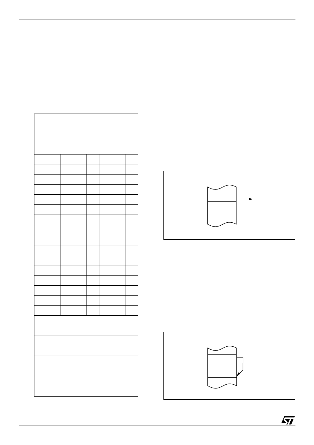
Data Transfers
Internal RAM. Table 6 shows the menu of in-
structions that are available for moving data
around within the internal memory spaces, and the
addressing modes that can be used with each
one. The MOV <dest>, <src> instruction allows
data to be transferred between any two internal
RAM or SFR locations without going through t he
Accumulator. Remember, the Uppe r 128 b ytes of
data RAM can be access ed only by indirect addressing, and SFR space only by di rect addressing.
Note: In uPSD321X Devices, the stack resides in
on-chip RAM, and grows upwards . The PUSH instruction first increments the St ack Pointer (SP),
then copies the byte into the stack. PUSH and
POP use only direct addressing to identify the byte
being saved or restored, but the stack itself is accessed by indirect addressing us ing the S P register. This means the stack can go into the Upper
128 bytes of RAM, if they are implemented, but not
into SFR space.
The Data Transfer instructions include a 16-bit
MOV that can be used to initialize the Data Pointer
(DPTR) for look-up tables in Program Memory.
The XCH A, <byte> instruction causes the Accumulator and ad-dressed byte to exchange data.
The XCHD A, @Ri instruction is similar, but only
the low nibbles are involved in the exchange. To
see how XCH and XCHD can be used to facilitate
data manipulations, cons ider first the problem of
shifting and 8-digit BCD number two digits to the
right. Table 8 shows how this can be done using
XCH instructions. To aid in understanding how the
code works, the contents of the regist ers that are
holding the BCD number and t he content of the
Accumulator are shown alongside each instruction
to indicate their status after the instruction has
been executed.
After the routine has been executed, the Accumulator contains the two digits that were shifted out
on the right. Doing the routine with direct MOVs
uses 14 code bytes. The same operation with
XCHs uses only 9 bytes and executes almost
twice as fast. To right-shift by an odd number of
digits, a one-digit must be executed. Table 9
shows a sample of code that will right-shift a BCD
number one digit, using the XCHD instruction.
Again, the contents of the registers holding the
number and of the accumulator are shown alongside each instruction.
Table 6. Data Transfer Instructions that Access Internal Data Memory Space
Mnemonic Operation
Dir. Ind. Reg. Imm
MOV A,<src> A = <src> XXXX
MOV <dest>,A <dest> = A X X X
MOV <dest>,<src> <dest> = <src> XXXX
MOV DPTR,#data16 DPTR = 16-bit immediate constant X
PUSH <src> INC SP; MOV “@SP”,<src> X
POP <dest> MOV <dest>,”@SP”; DEC SP X
XCH A,<byte> Exchange contents of A and <byte> X X X
XCHD A,@Ri Exchange low nibbles of A and @Ri X
Addressing Modes
24/152

UPSD3212C, UPSD3212CV
First, pointers R1 and R0 are set up to point to the
two bytes containing the last four BCD digits. Then
Table 7. Shifting a BCD Number Two Digits to the Right (using direct MOVs: 14 bytes)
a loop is executed which leaves the last byte, location 2EH, holding the l ast two dig its of the shi fted
number. The pointers are decremented, and the
loop is repeated for location 2DH. The CJNE instruction (Compare and Jump if Not equal) is a
loop control that will be described later. The l oop
MOV A,2Eh 00 12 34 56 78 78
MOV 2Eh,2 Dh 00 12 34 56 56 78
MOV 2Dh,2 Ch 00 12 34 34 56 78
executed from LOOP to CJNE for R1 = 2EH, 2DH,
2CH, and 2BH. At that point the digit that was originally shifted out on the right has propagated to location 2AH. Since that location should be left with
MOV 2Ch,2 Bh 00 12 12 34 56 78
MOV 2Bh,# 0 00 00 12 34 56 78
0s, the lost digit is moved to the Accumulator.
Table 8. Shifting a BCD Number Two Digits to the Right (using direct XCHs: 9 bytes)
CLR A 00 12 34 56 78 00
XCH A,2Bh 00 0 0 34 56 78 12
XCH A,2Ch 00 00 12 56 78 34
XCH A,2Dh 00 00 12 34 78 56
XCH A,2Eh 00 0 0 12 34 56 78
Table 9. Shifting a BCD Number One Digit to the Right
2A 2B 2C 2D 2E ACC
MOV R1,#2Eh 00 12 34 56 78 xx
MOV R0,#2Dh 00 12 34 56 78 xx
2A 2B 2C 2D 2E ACC
2A 2B 2C 2D 2E ACC
; loop for R1 = 2Eh
LOOP: MOV A,@R1 00 12 34 56 78 78
XCHD A,@R0 00 12 34 58 78 76
SWAP A 00 12 34 58 78 67
MOV @R1,A 0012345867 67
DEC R1 00 12 34 58 67 67
DEC R0 00 12 34 58 67 67
CNJE R1,#2Ah,LOOP 00 12 34 58 67 67
; loop for R1 = 2Dh 00 12 38 45 67 45
; loop for R1 = 2Ch 00 18 23 45 67 23
; loop for R1 = 2Bh 08 01 23 45 67 01
CLR A 0801234567 00
XCH A,2Ah 00 01 23 45 67 08
25/152
UPSD3212C, UPSD3212CV
External RAM. Table 10 shows a l ist of t he Data
Transfer instructions that access external Data
Memory. Only indirect addressing can be used.
The choice is whether t o use a one-byte address,
@Ri, where Ri can be either R0 or R1 of the s elected register bank, or a two-byte
address, @DTPR.
Note: In all external Data RAM accesses, the Accumulator is always either the destination or
source of the data.
Lookup Tables. Ta ble 1 1 shows t he tw o instructions that are available for reading lookup tables in
Program Memory. Since these instructions access
only Program Memory, the lookup tables can only
be read, not updated.
The mnemonic is MOVC for “move constant.” The
first MOVC instruction in Table 11 can accommodate a table of up to 256 entries numbered 0
through 255. The number of th e desired entry is
loaded into the Accumulator, and the Data Pointer
is set up to point to the beginning of the table.
Then:
MOVC A, @A+DPTR
copies the desired table entry into the Accumula-
tor.
The other MOVC instruction works the same way,
except the Program Counter (PC) is used as the
table base, and the table is accessed through a
subroutine. First the num ber of the desired en-try
is loaded into the Accumulator, and the subroutine
is called:
MOV A , ENTRY NUMBER
CALL TABLE
The subroutine “TABLE” would look like this:
TABLE: MOVC A , @A+PC
RET
The table itself immediately follows the RET (return) instruction is Program Memory. This type of
table can have up to 255 entries, numbered 1
through 255. Number 0 cannot b e used, because
at the time the MOVC instruction is execute d, the
PC contains the address of the RET instruction.
An entry numbered 0 would be the RET opcode itself.
Table 10. Data Transfer Instruction that Access External Data Memory Space
Address Width Mnemonic Operation
8 bits MOVX A,@Ri READ external RAM @Ri
8 bits MOVX @Ri,A WRITE external RAM @Ri
16 bits MOVX A,@DPTR READ external RAM @DPTR
16 bits MOVX @DPTR,a WRITE external RAM @DPTR
Table 11. Lookup Table READ Instruction
Mnemonic Operation
MOVC A,@A+DPTR READ program memory at (A+DPTR)
MOVC A,@A+PC READ program memory at (A+PC)
26/152
Boolean Instructions
The uPSD323X Devices contain a complete Boolean (single-bit) processor. One page o f the internal RAM contains 128 address able bits, and the
SFR space can support up to 128 addressable bits
as well. All of the port lines are bit-addressable,
and each one can be treated as a separate singlebit port. The instructions that access these bits are
not just conditional branches, but a complete
menu of move, set, clear, complement, OR and
AND instructions. These kinds of bit operations
are not easily obtained in other architectures with
any amount of byte-oriented software.
The instruction set for the Boolean processor is
shown in Table 12. All bit s acc esse s are by di rect
addressing.
Bit addresses 00h through 7Fh are in the Lower
128, and bit addresses 80h through FFh are in
SFR space.
Note how easily an internal flag can be moved to
a port pin:
MOV C,FLAG
MOV P1.0,C
In this example, FLAG is the name of any addressable bit in the Lower 128 or SFR space. An I/O
line (the LSB of Port 1, in this case) is set or
cleared depending on whether the Flag Bit is '1' or
'0.'
The Carry Bit in the PSW is used as the single-bit
Accumulator of the Boolean processor. Bit instructions th at re fer to th e Ca rry B it as C as se mbl e a s
Carry-specific instructions (CLR C, etc.). The Carry Bit also has a direct address, since it resides in
the PSW register, which is bit-addressable.
Note: The Boolean instruction set includes ANL
and ORL operations, but not the XRL (Exclusive
OR) operation. An XRL operation is simple to implement in software. Suppose, for example, it is required to form the Exclusive OR of two bits:
C = bit 1 .XRL. bit2
The software to do that could be as follows:
MOV C , bit1
JNB bit2, OVER
CPL C
OVER: (continue)
First, Bit 1 is moved to the Carry. If bit2 = 0, then
C now contains the correct result. That i s, Bit 1
.XRL. bit2 = bit1 if bit2 = 0. On the o ther hand, if
bit2 = 1, C now contains the complement of the
correct result. It need only be inverted (CPL C) to
complete the operation.
This code uses the JNB instruction, one of a series
of bit-test instructions which execute a jump if the
UPSD3212C, UPSD3212CV
addressed bit is set (JC, JB, JBC) or if the addressed bit is not set (JNC, JNB). In the above
case, Bit 2 is being tested, and if bit2 = 0, the CPL
C instruction is jumped over.
JBC executes the jump if the addressed bit is set,
and also clears the bit. Thus a flag can be tested
and cleared in one operation. All the PSW bits are
directly addressable, so the Parity Bit, or the general-purpose flags, for example, are also available
to the bit-test instructions.
Relative Offset
The destination address for thes e jumps is specified to the assembler by a label or by an actual address in Program memory. How-ever, the
destination address assembl es to a relative of fset
byte. This is a signed (two’s complement) offset
byte which is added to the PC in two’s complement
arithmetic if the jump is executed.
The range of the jump is therefore -128 to +127
Program Memory bytes relative to the first byte following the instruction.
Table 12. Boolean Instructions
Mnemonic Operation
ANL C,bit C = A .AND. bit
ANL C,/bit C = C .AND. .NOT. bit
ORL C,bit C = A .OR. bit
ORL C,/bit C = C .OR. .NOT. bit
MOV C,bit C = bit
MOV bit,C bit = C
CLR C C = 0
CLR bit bit = 0
SETB C C = 1
SETB bit bit = 1
CPL C C = .NOT. C
CPL bit bit = .NOT. bit
JC rel Jump if C =1
JNC rel Jump if C = 0
JB bit,rel Jump if bit =1
JNB bit,rel Jump if bit = 0
JBC bit,rel Jump if bit = 1; CLR bit
27/152

UPSD3212C, UPSD3212CV
Jump Instructions
Table 13 shows the list of unconditional jump instructions. The table lists a single “JMP add” instruction, but in fact there a re th ree S JMP, LJMP,
and AJMP, which differ in the format of the destination address. JMP is a generic mnemonic which
can be used if the programmer does not care
which way the jump is en-coded.
The SJMP instruction encodes the destination address as a relative offset, as described above. The
instruction is 2 bytes long, consisting of the opcode and the relative offset byte. The jump distance is limited to a range of -128 to +127 bytes
relative to the instruction following the SJMP.
The LJMP instruction encodes the destination address as a 16-bit constant. The instruction is 3
bytes long, consistin g of the op code and two address bytes. The des tination address can be anywhere in the 64K Program Memory space.
The AJMP instruction encodes the destination address as an 11-bit constant. The instruction is 2
bytes long, consisting of the opcode, which itself
contains 3 of the 11 address bits, followed by another byte containing the low 8 bits of the destination address. When the instruction is executed,
these 11 bits are simply substituted for the low 11
bits in the PC. The high 5 bits stay the same.
Hence the destination has to be within the same
2K block as the instruction following the AJMP.
In all cases the programmer specifies the destination address to the assembler in the same way: as
a label or as a 16-bit constant. The assembler will
put the destination address into the correct format
for the given instruction. If the format required by
the instruction will not support t he distance t o the
specified destination address, a “Destination out
of range” message is written into the List file.
The JMP @A+DPTR instruction supports case
jumps. The destination address is computed at execution time as the sum of the 16-bit DPTR register and the Accumulator. Typically. DPTR is set up
with the address of a jump table. In a 5-way
branch, for ex-ample, an integer 0 through 4 is
loaded into the Accum ulator. The code t o be executed mi ght be as follows:
MOV DPTR, # J U MP TABLE
MOV A,INDEX_ NU MBER
RL A
JMP @A+DPTR
The RL A instruction converts the index number (0
through 4) to an even number on the range 0
through 8, because each entry in the jump table is
2 bytes long:
JUMP TABLE:
AJMP CASE 0
AJMP CASE 1
AJMP CASE 2
AJMP CASE 3
AJMP CASE 4
Table 13 shows a single “CALL a ddr” instruction,
but there are two of them, LCALL and ACALL,
which differ in the format in which the subroutine
address is given to the CPU. CALL is a generic
mnemonic which can b e used if the progra mmer
does not care which way the address is encoded.
The LCALL instruction uses the 16-bit address format, and the subroutine can be anywh ere in the
64K Program Memory space. The ACALL instruction uses the 11-bit format, and the subroutine
must be in the same 2K block as the instruction following the ACALL.
In any case, the programmer specifies the subroutine address to the assembler in the same way: as
a label or as a 16-bit constant. The assembler will
put the address into the correct format for the given instructions.
Subroutines should end with a RET instruction,
which returns execution to the instruction following
the CALL.
RETI is used to return from an interrupt service
routine. The only difference between RET and
RETI is that RET I tells the interrupt control system
that the interrupt in progress is done. If there is no
interrupt in progress at the time RETI is executed,
then the RETI is functionally identical to RET.
Table 13. Unconditional Jump Instructions
Mnemonic Operation
JMP addr Jump to addr
JMP @A+DPTR Jump to A+DPTR
CALL addr Call Subroutine at addr
RET Return from subroutine
RETI Return from Interrupt
28/152
NOP No operation
UPSD3212C, UPSD3212CV
Table 14 shows the list of conditional jumps available to the uPSD321X Devices user. All of these
jumps specify the destination address by the relative offset method, and so are limited to a jump distance of -128 to +127 bytes from the instruction
following the conditional jump instruction. Important to note, however, the user specifies to the assembler the actual destination address the sam e
way as the other jumps: as a label or a 16-bit constant.
There is no Zero Bit in the PSW. The JZ and JNZ
instructions test the Accumulator data for that condition.
The DJNZ instruction (Decrement and Jump if Not
Zero) is for loop control. To execute a loop N
times, load a counter byte with N and terminate the
loop with a DJNZ to the b eginning of t he loop, as
shown below for N = 10:
MOV COUNTER,#10
LOOP: (begin loop)
•
•
•
(end loop)
DJNZ COUNTER, LOOP
(continue)
The CJNE instruction (Compare and Jump if Not
Equal) can also be used f or loo p cont rol a s in Table 9. Two bytes are specified in the operand field
of the instruction. The jump is executed only if the
two bytes are not equal. In the example of Table 9
Shifting a BCD Numb er One Digits to the Right,
the two bytes were data in R1 and the constant
2Ah. The initial data in R1 was 2Eh.
Every time the loop was executed, R1 was decremented, and the looping was to continue until the
R1 data reached 2Ah.
Another application of this instruction is in “greater
than, less than” comparisons. The two bytes in the
operand field are taken as unsigned integers. If the
first is less than the second, then the Carry Bit is
set (1). If the first is greater than or equal to the
second, then the Carry Bit is cleared.
Machine Cycles
A machine cycle consists of a sequence of six
states, numbered S1 through S6. Each state time
lasts for t wo oscillator peri ods. Thus, a ma chine
cycle takes 12 oscillator periods or 1µs if the oscillator frequency is 12MHz. Refer to Figure 14, page
30.
Each state is divided into a Phase 1 half and a
Phase 2 half. State Sequence i n uPSD321X Devices shows that retrieve/execute sequences in
states and phases for various kinds of instructions.
Normally two program retrievals are generated
during each machine cycle, even if the instruction
not
being executed does
require it. If the instruction being executed does not need more code
bytes, the CPU simply ig nores the e xtra retrieval,
and the Program Counter is not incremented.
Execution of a one-cycle instruction (Figure 14,
page 30) begins during State 1 of the machine cycle, when the opcode is latched into the Instruction
Register. A second retrieve occurs during S4 of
the same machine cycle. Execution is complete at
the end of State 6 of this machine cycle.
The MOVX instructions take two machine cycles
to execute. No program retrieval is generated during the second cycle of a MOVX instruction. This
is the only time program retrievals are skipped.
The retrieve/execute sequence for MOVX instruction is shown in Figure 14, page 30 (d).
Table 14. Conditional Jump Instructions
Addressing Modes
Mnemonic Operation
Dir. Ind. Reg. Imm
JZ rel Jump if A = 0 Accumulator only
JNZ rel Jump if A ≠ 0 Accumulator only
DJNZ <byte>,rel Decrement and jump if not zero X X
CJNE A,<byte>,rel Jump if A ≠ <byte> X X
CJNE <byte>,#data,rel Jump if <byte> ≠ #data X X
29/152
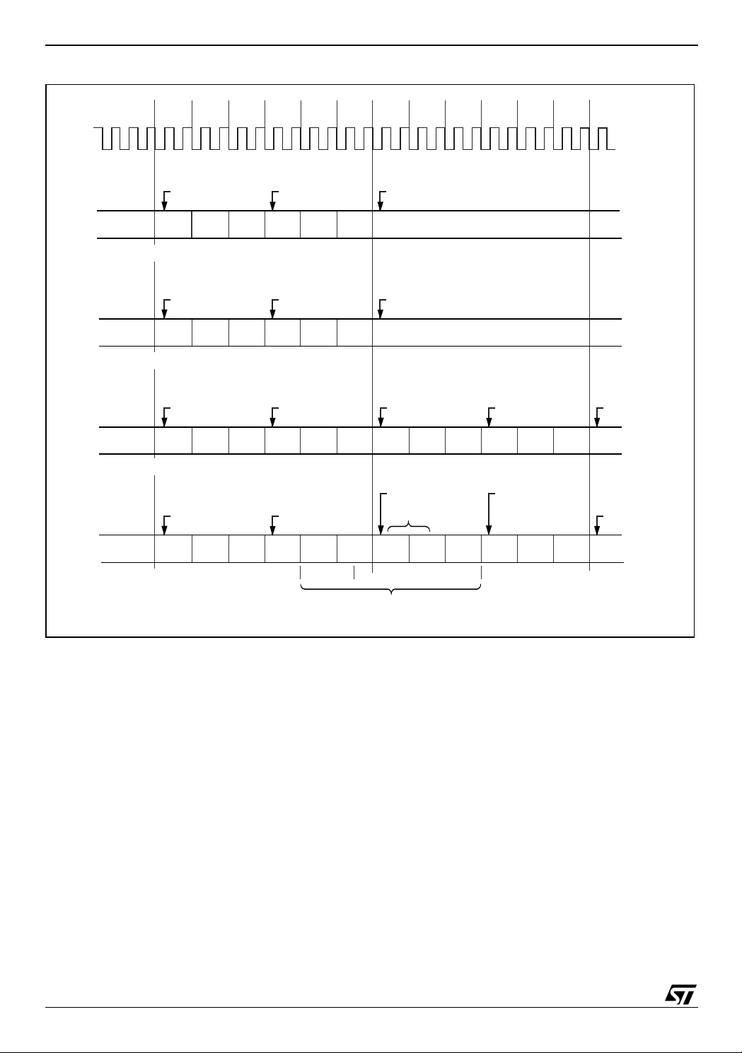
UPSD3212C, UPSD3212CV
Figure 14. State Sequence in uPSD321X Devices
Osc.
(XTAL2)
a. 1-Byte, 1-Cycle Instruction, e.g. INC A
b. 2-Byte, 1-Cycle Instruction, e.g. ADD A, adrs
c. 1-Byte, 2-Cycle Instruction, e.g. INC DPTR
S1 S2 S3 S4 S5 S6 S1 S2 S3 S4 S5 S6
p1 p1 p1 p1 p1 p1 p1 p1 p1 p1 p1 p1p2 p2 p2 p2 p2 p2 p2 p2 p2 p2 p2 p2
Read next
Read opcode
S1 S2 S3 S4 S5 S6
Read opcode
S1 S2 S3 S4 S5 S6
Read opcode
S1 S2 S3 S4 S5 S6
Read opcode
(MOVX)
opcode and
discard
Read 2nd
Byte
Read next
opcode and
discard
Read next
opcode and
discard
Read next
opcode
Read next
opcode
Read next
opcode and
discard
S1 S2 S3 S4 S5 S6
No Fetch
No ALE
Read next
opcode and
discard
No Fetch
Read next
opcode
Read next
opcode
S1 S2 S3 S4 S5 S6 S1 S2 S3 S4 S5 S6
d. 1-Byte, 2-Cycle MOVX Instruction
Addr Data
Access External Memory
AI06822
30/152
 Loading...