

SGS Thomson Microelectronics ULQ2805A, ULQ2804A, ULQ2803A, ULQ2802A, ULQ2801A Datasheet

.EIGHT DARLINGTONSPER PACKAGE
.EXTENDEDTEMPERATURE RANGE
(– 40 to 105°C)
.OUTPUTCURRENT TO 500mA
.OUTPUTVOLTAGETO50V
.INTEGRALSUPPRESSIONDIODES
.VERSIONSFOR ALL POPULARLOGICFAMI-
LIES
.OUTPUTCANBE PARALLELED
.INPUTS PINNED OPPOSITE OUTPUTS TO
SIMPLIFYBOARDLAYOUT
ULQ 2801A
ULQ2802A - ULQ2803A
ULQ2804A - ULQ2805A
EIGHTDARLINGTON ARRAYS
DIP18
(PlasticPackage)
DESCRIP TION
TheULQ2801A-ULQ2805Aeachcontaineightdarlington transistorswith common emitters and integral suppression diodes for inductive loads. Each
darlington features a peak load current rating of
600mA (500mA continuous)and can withstand at
least50Vin theoffstate.Outputsmaybeparalleled
for highercurrent capability.
Fiveversionsare availableto simplify interfacingto
standardlogic families: theULQ2801Ais designed
for generalpurposeapplicationswitha current limit
resistor; theULQ2802Ahasa 10.5kΩinputresistor
and zenerfor14-25VPMOS; theULQ2803Ahasa
2.7kΩ input resistor for 5V TTL and CMOS ; the
ULQ2804Ahas a 10.5kΩ input resistor for 6-15V
CMOS and the ULQ2805A is designed to sink a
minimumof 350mAfor standardand SchottkyTTL
wherehigheroutput currentis required.
Alltypes are suppliedin a 18-leadplastic DIP with
a copper lead frameand feature the convenientinput-opposite-outputpinout to simplifyboard layout.
April1993
PIN CONNECTI ON (top view)
1/8

ULQ2801A - ULQ2802A - ULQ2803A - ULQ2804A - ULQ2805A
SCHEMATIC DIA G RAM AND ORDER CODES
ForULQ2801A(eachdriver forPMOS-CMOS)For ULQ2802A(each driver for14-15 V PMOS)
For ULQ2803A(eachdriver for 5V, TTL/CMOS) For ULQ2804A (each driver for 6-15 V
CMOS/PMOS
For ULQ2805A(eachdriver for highout TTL)
ABSOLUTE MAXIMUM RATINGS
Symbol Parameter Value Unit
V
o
V
I
C
I
B
P
tot
T
amb
T
stg
Output Voltage 50 V
Input Voltage for ULQ2802A, 2803A, 2804A
i
for ULQ2805A
30
15
Continuous Collector Current 500 mA
Continuous Base Current 25 mA
Power Dissipation (one Darlington pair)
(total package)
1.0
2.25
Operating Ambient Temperature Range – 40 to 105 °C
Storage Temperature Range – 55 to 150 °C
V
V
W
W
THERMAL DATA
Symbol Parameter Value Unit
Thermal Resistance Junction-ambient Max. 55 °C/W
2/8
R
th j-amb
ULQ2801A - ULQ2802A - ULQ2803A - ULQ2804A - ULQ2805A
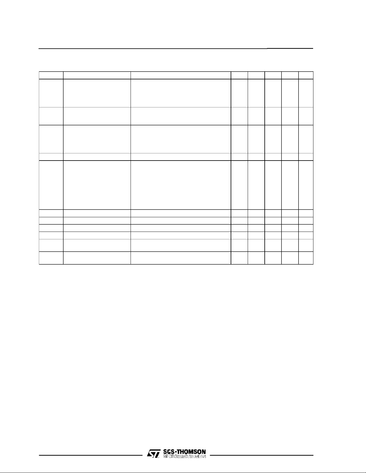
ELECTRICAL CHARACTERISTICS (Tj= –40 to 105oC, unless otherwise specified)
Symbol Parameter Test Conditions Min. Typ. Max. Unit Fig.
I
V
CE (sat)
I
I
V
h
t
t
(*) Guaranteed by desi gn
Output Leakage Current VCE= 50V
CEX
Collector-emitter
Saturation Voltage
Input Current for ULQ2802A Vi= 17V
i(on)
Input Current TJ= 105°C, IC= 500µA5065µA4
i(off)
Input Voltage for ULQ2802A VCE= 2V, Ic= 300mA
i(on)
DC Forward Current Gain for ULQ2802A VCE= 2V, Ic= 350mA 1000 – 2
FE
C
Input Capacitance 15 25 (*) pF –
i
Turn-on Delay Time 0.5 Vito 0.5 V
PLH
Turn-off Delay Time 0.5 Vito 0.5 V
PHL
I
Clamp Diode Leakage
R
Current
V
Clamp Diode Forward
F
Voltage
= 105°C, VCE= 50V
T
J
= 105°C
T
J
for ULQ2802A V
for ULQ2804A V
= 50V, Vi=6V
CE
= 50V, Vi=1V
CE
IC= 100mA, IB= 250µA
= 200mA, IB= 350µA
I
C
= 350mA, IB= 500µA
I
C
0.82
for ULQ2803A V
for ULQ2804A V
for ULQ2805A V
for ULQ2803A V
for ULQ2804A V
for ULQ2805A V
= 3.85V
i
=5V
i
= 12V
V
i
=3V
i
= 2V, Ic= 200mA
CE
= 2V, Ic= 250mA
V
CE
= 2V, Ic= 300mA
V
CE
= 2V, Ic= 125mA
CE
= 2V, Ic= 200mA
V
CE
= 2V, Ic= 275mA
V
CE
= 2V, Ic= 350mA
V
CE
= 2V, Ic= 350mA
CE
o
o
0.93
0.35
0.25 1 (*) µs–
0.25 1 (*) µs–
VR= 50V
= 105°C, VR= 50V
T
J
IF= 350mA 1.7 2 V 7
0.9
1.1
1.3
1
1.5
50
100
500
500
1.1
1.3
1.6
1.25
1.35
0.5
1.45
2.4
13
2.4
2.7
3
5
6
7
8
2.4
50
100µAµA
µA
µA
µA
µA
V
V
V
mA
mA
mA
mA
mA
V
V
V
V
V
V
V
V
V
1a
1a
1b
1b
2
3
5
6
3/8
 Loading...