

SGS Thomson Microelectronics ULN2803A, ULN2801A, ULN2802A, ULN2805A, ULN2804A Datasheet
.EIGHTDARLINGTONSWITHCOMMONEMIT-
TERS
.
OUTPUTCURRENT TO 500 mA
.OUTPUTVOLTAGETO 50 V
.
INTEGRALSUPPRESSIONDIODES
.VERSIONSFOR ALL POPULARLOGICFAMI-
LIES
.OUTPUTCAN BE PARALLELED
.INPUTS PINNED OPPOSITE OUTPUTS TO
SIMPLIFYBOARDLAYOUT
ULN 2801A
ULN 2802A - ULN2803A
ULN 2804A - ULN2805A
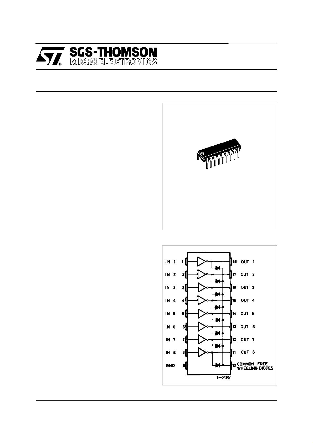
EIGHTDARLINGTONARRAYS
DIP18
DESCRI PT I ON
TheULN2801A-ULN2805Aeachcontaineightdarlingtontransistorswith common emitters and integral suppression diodes for inductive loads. Each
darlington features a peak load current rating of
600mA (500mA continuous)and can withstand at
least50Vintheoffstate.Outputsmaybeparalleled
forhighercurrentcapability.
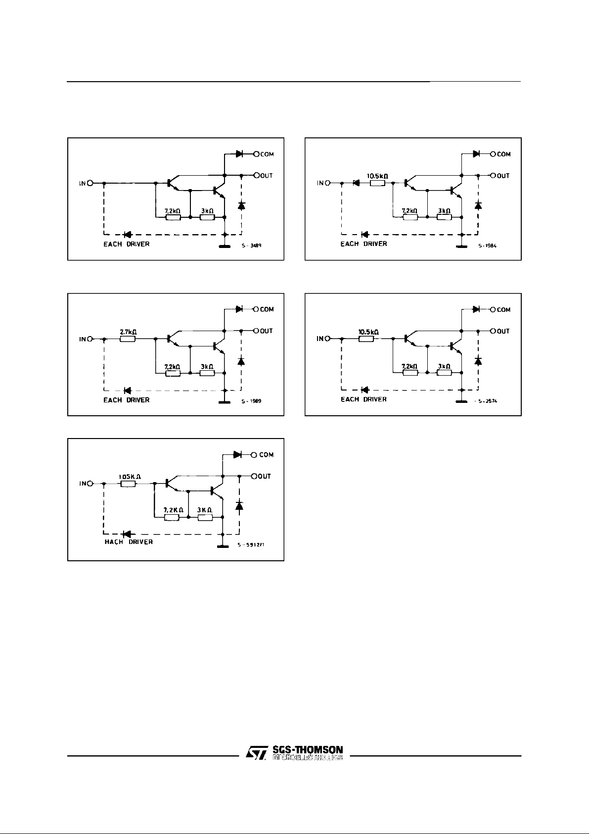
Fiveversionsareavailableto simplifyinterfacingto
standardlogicfamilies: the ULN2801Aisdesigned
forgeneralpurposeapplicationswitha currentlimit
resistor; theULN2802Ahasa 10.5kΩinputresistor
andzenerfor14-25VPMOS; theULN2803Ahas a
2.7kΩ input resistor for 5V TTL and CMOS ; the
ULN2804A has a 10.5kΩ input resistor for 6-15V
CMOS and the ULN2805A is designed to sink a
minimum of350mA for standardandSchottkyTTL
wherehigheroutputcurrent is required.
All types are supplied in a 18-leadplastic DIP with
acopperleadfromandfeaturetheconvenientinputopposite-outputpinoutto simplifyboardlayout.
PIN CONNECTI O N (top view)
September 1997
1/8
ULN2801A - ULN2802A - ULN2803A - ULN2804A - ULN2805A
SCHEMATIC DIAGRAM AND OR DER CODES
ForULN2801A(eachdriver for PMOS-CMOS) For ULN2802A(eachdriver for 14-15V PMOS)
ForULN2803A(eachdriver for 5 V, TTL/CMOS)
ForULN2805A(eachdriver for highout TTL)
For ULN2804A (each driver for 6-15 V
CMOS/PMOS
2/8
ULN2801A - ULN2802A - ULN2803A - ULN2804A - ULN2805A
ABSOLUTE MAXIMUM RATINGS
Symbol Parameter Value Unit
V
o
V
I
C
I
B
P
tot
T
amb
T
stg
Tj Junction Temperature Range – 20 to 150 °C
THERMAL DATA
Symbol Parameter Value Unit
R
th j–amb
Output Voltage 50 V
Input Voltage
i
for ULN2802A, UL2803A, ULN2804A
for ULN2805A
30
15
Continuous Collector Current 500 mA
Continuous Base Current 25 mA
Power Dissipation
(one Darlington pair)
(total package)
1.0
2.25
Operating Ambient Temperature Range – 20 to 85
Storage Temperature Range – 55 to 150 °C
Thermal Resistance Junction-ambient Max. 55
°
C/W
°
V
W
C
ELECTRICAL CHARACTERISTICS
=25oC unless otherwise specified)
(T
amb
Symbol Parameter Test Conditions Min. Typ. Max. Unit Fig.
I
CEX
V
CE(sat)
I
i(on)
I
i(off)
V
i(on)
h
C
t
PLH
t
PHL
I
V
Output Leakage Current VCE= 50V
=70°C, VCE= 50V
T
amb
=70°C
T
amb
for ULN2802A
for ULN2804A
Collector-emitter
Saturation Voltage
IC= 100mA, IB= 250µA
I
I
Input Current for ULN2802A Vi= 17V
for ULN2803A V
for ULN2804A V
for ULN2805A V
Input Current T
= 50V, Vi=6V
V
CE
= 50V, Vi=1V
V
CE
0.9
= 200mA, IB= 350µA
C
= 350mA, IB= 500µA
C
1.1
1.3
0.82
= 3.85V
i
=5V
i
= 12V
V
i
=3V
i
=70°C, IC= 500µA5065
amb
0.93
0.35
1.5
1
Input Voltage VCE=2V
for ULN2802A
= 300mA
I
C
for ULN2803A
= 200mA
I
C
= 250mA
I
C
= 300mA
I
C
for ULN2804A
= 125mA
I
C
= 200mA
I
C
= 275mA
I
C
= 350mA
I
C
for ULN2805A
= 350mA
I
C
DC Forward Current Gain for ULN2801A
FE
Input Capacitance 15 25 pF –
i
Turn-on Delay Time 0.5 Vito 0.5 V
Turn-off Delay Time 0.5 Vito 0.5 V
Clamp Diode Leakage Current VR= 50V
R
Clamp Diode Forward Voltage IF= 350mA 1.7 2 V 7
F
T
= 2V, IC= 350mA 1000 – 2
V
CE
0.25 1
0.25 1 µs–
=70°C, VR= 50V
amb
o
o
50
100
500
500
1.1
1.3
1.6
1.25
1.35
0.5
1.45
2.4
13
2.4
2.7
3
5
6
7
8
2.4
50
100
µA
µA
A
µ
A
µ
V
V
V
mA
mA
mA
mA
mA
A4
µ
V
V
V
V
V
V
V
V
V
s–
µ
µA
A66
µ
1a
1a
1b
1b
2
3
5
3/8
 Loading...