

SGS Thomson Microelectronics ULN2077B, ULN2075B, ULN2071B, ULN2069B, ULN2067B Datasheet
...
80 V - 1.5 AQUAD DARLINGTONSWITCHES
.OUTPUT CURRENT TO 1.5 A EACH DAR-
LINGTON
.MINIMUMBREAKDOWN80 V
.SUSTAININGVOLTAGEAT LEAST50V
.INTEGRAL SUPPRESSION DIODES
(ULN2065B, ULN2067B, ULN2069B and
ULN2071B)
.ISOLATEDDARLINGTONPINOUT(ULN2075B
and ULN2077B)
.VERSIONS COMPATIBLE WITH ALL POPU-
LARLOGIC FAMILIES
DESCRIP TION
Designedto interfacelogic to a widevariety of high
current,highvoltageloads,thesedeviceseachcontain four NPN darlington switches delivering up to
1.5 A with a specifiedminimumbreakdownof 80 V
and a sustainingvoltage of 50 V. The ULN2065B,
ULN2067B,ULN2069BandULN2071Bcontainintegral suppression diodes for inductive loads and
have common emitters ; the ULN2075B and
ULN2077Bfeature isolateddarlington pinoutsand
are intended for applications such as emitter follower configurations. Inputs of the ULN2065B,
ULN2069B and ULN2075B are compatible with
popular 5 V logic families and the ULN2067B,
ULN2071Band ULN2077Bare compatible with 615 VCMOS and PMOS. The ULN2069B and
ULN2071Bincludea predriverstageto provideextragain,reducingthe loadon controllogic.
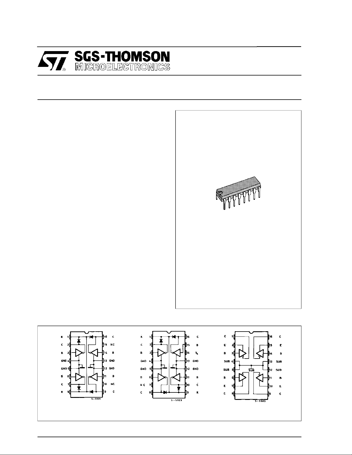
ULN2065B - ULN2067B
ULN2069B - ULN2071B
ULN2075B - ULN2077B
POWERDIP
12 + 2 + 2
PIN CONNECTIONS AND ORDER CO DES
ULN2065B
ULN2067B
April1993
ULN2069B
ULN2071B
ULN2075B
ULN2077B
1/7
ULN2065B-ULN2067B-ULN2069B-ULN2071B-ULN2075B-ULN2077B
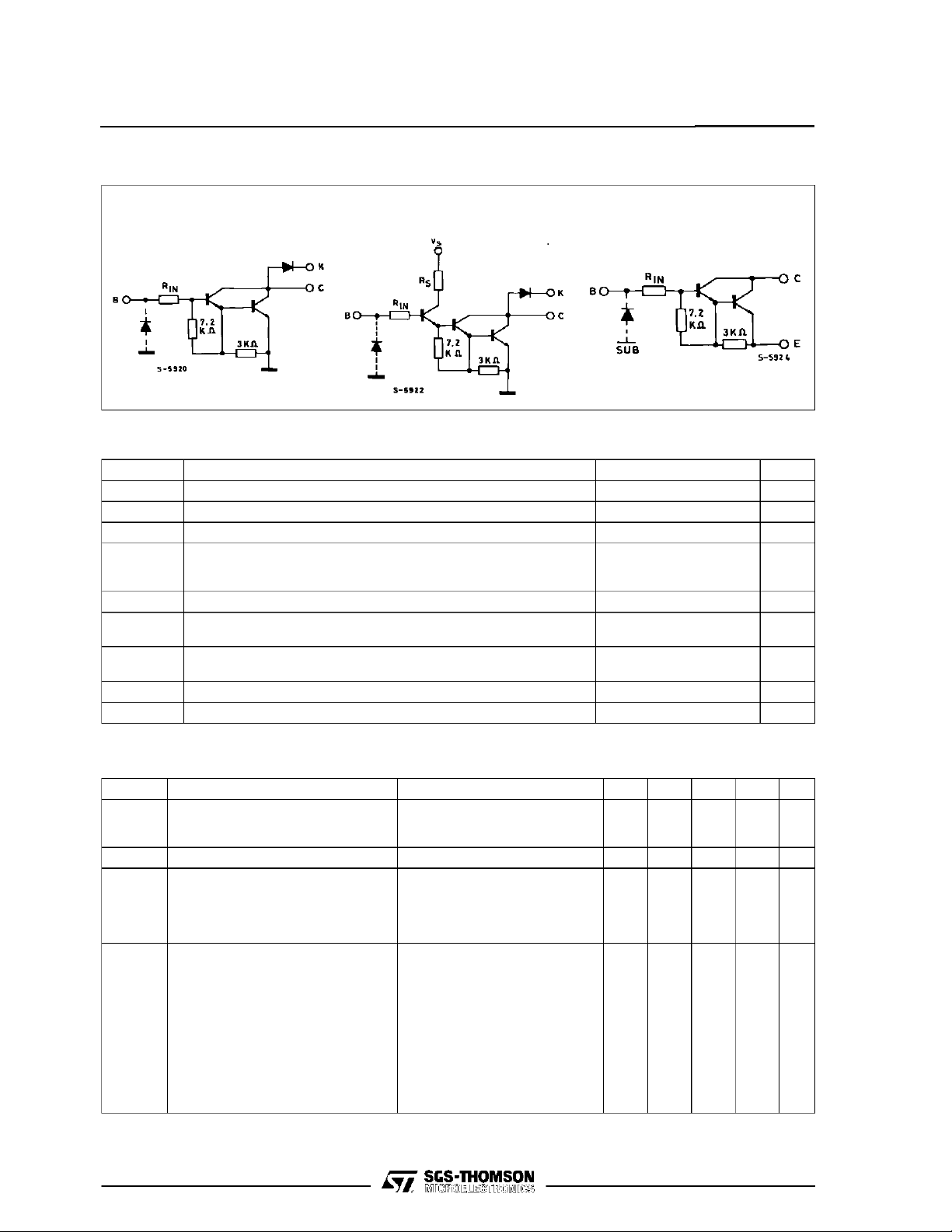
SCHEMATIC DIAG RAM
ULN2065B : RIN=350Ω
ULN2067B : R
IN
=3kΩ
ULN2069B : R
ULN2071B : R
=2.5kΩ,Rs=900Ω
IN
= 11.6kΩ,Rs=3.4kΩ
IN
ULN2075B : R
ULN2077B : R
= 350Ω
IN
=3kΩ
IN
ABSOLUTE MAXIMUM RATINGS
Symbol Parameter Value Unit
V
V
CE(sus)
P
T
T
CEX
I
O
V
I
V
amb
stg
tot
Output Voltage 80 V
Output Sustaining Voltage 50 V
Output Current 1.75 A
Input Voltage for ULN2075B – 2077B
i
for ULN2067B – 2071B
for ULN2065B – 2069B
Input Current 25 mA
I
Supply Voltage for ULN2069B
s
Power Dissipation at T
for ULN2071B
=90°C
pins
amb
=70°C
at T
60
30
15
10
20
4.3
1
Operating Ambient Temperature Range – 20 to 85 °C
Storage Temperature – 55 to 150 °C
V
V
V
V
V
W
W
ELECTRICAL CHARACTERISTICS (T
=25oC unless otherwise specified )
amb
Symbol Parameter Test Conditions Min. Typ. Max. Unit Fig.
I
V
CE(sus)
V
CE(sat)
I
Output Leakage Current VCE= 80V
CEX
T
T
amb
amb
=25°C
=70°C
Collector-emitter Sustaining Voltage IC= 100mA, Vi= 0.4V 50 V 2
Collector-emitter Saturation Voltage IC= 500mA IB= 625µA
= 750mA IB= 935µA
I
C
=1A IB= 1.25mA
I
C
= 1.25A IB= 2mA
I
C
= 1.5A IB= 2.25mA
I
C
Input Current for ULN2065B and ULN2075B
i(on)
= 2.4V
V
i
= 3.75V
V
i
for ULN2067B and ULN2077B
=5V
V
i
= 12V
V
i
for ULN2069B
= 2.75V
V
i
= 3.75V
V
i
for ULN2071B
=5V
V
i
= 12V
V
i
1.4
3.3
0.6
1.7
100
500µAµA
1.1
1.2
1.3
1.4
1.5
4.3
mA
9.6
mA
1.8
mA
5.2
mA
5.5
mA
10
mA
4
mA
12.5
mA
V
V
V
V
V
2/7
1
3
3
3
3
3
4
4
4
4
4
4
4
4
ULN2065B-ULN2067B-ULN2069B-ULN2071B-ULN2075B-ULN2077B
ELECTRICAL CHARACTERISTICS (T
=25oC unless otherwise specified ) (continued)
amb
Symbol Parameter Test Conditions Min. Typ. Max. Unit Fig.
V
t
t
Notes : 1. Input voltage is with reference to the substrate (no connection to any other pins) for the ULN2075B and ULN2077B
Input Voltage VCE= 2V, IC=1A
i(on)
ULN2065B, ULN2075B
ULN2067B, ULN2077B
= 2V, IC= 1.5A
V
CE
ULN2065B, ULN2075B
ULN2067B, ULN2077B
ULN2069B
ULN2071B
Supply Current for ULN2069B
I
s
Turn-on Delay Time 0.5 Vito 0.5 V
PLH
Turn-off Delay Time 0.5 Vito 0.5 V
PHL
Clamp Diode Leakage Current for ULN2065B-ULN2067B
I
R
Clamp Diode Forward Voltage for ULN2065B-ULN2067B
V
F
reference is ground for all other types.
2. Input current may be limited by maximum allowable input voltage.
= 500mA, Vi= 2.75V
I
C
for ULN2071B
= 500mA, Vi=5V
I
C
and ULN2069B-ULN2071B
=80V
V
R
T
T
amb
amb
=25°C
=70°C
and ULN2069B-ULN2071B
=1A
I
F
= 1.5 A
I
F
2
V
6.5
2.5
10
2.75
5
5
V
5
V
5
V
5
V
5
V
5
6
4.5mAmA88
o
o
1 µs
1.5 µs
6
50
100µAµA
7
1.752V
V
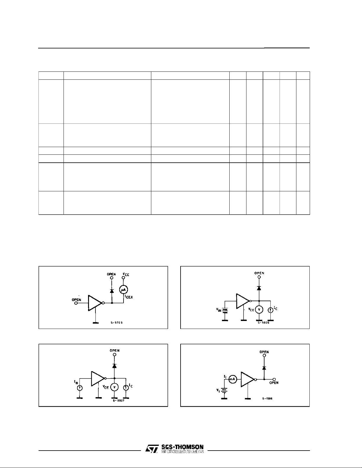
TEST CIRCUITS
Figure 1. Figure2.
Figure 3. Figure4.
3/7
 Loading...