

Datasheet TS556IN, TS556ID, TS556I, TS556CD, TS556CN Datasheet (SGS Thomson Microelectronics)
...
.
VERYLOW POWERCONSUMPTION:
.
100µA typat VCC=5V
.
HIGH MAXIMUM ASTABLE FREQUENCY
2.7MHz
.
PIN-TO-PINAND FUNCTIONALLY
COMPATIBLEWITH BIPOLARNE555
.
VOLTAGERANGE : +2Vto +18V
.
HIGHOUTPUT CURRENT CAPABILITY
.
SUPPLY CURRENT SPIKES REDUCED
DURING OUTPUTTRANSITIONS
.
HIGHINPUT IMPEDANCE: 1012Ω
.
OUTPUT COMPATIBLE WITH TTL,CMOS
ANDLOGIC MOS
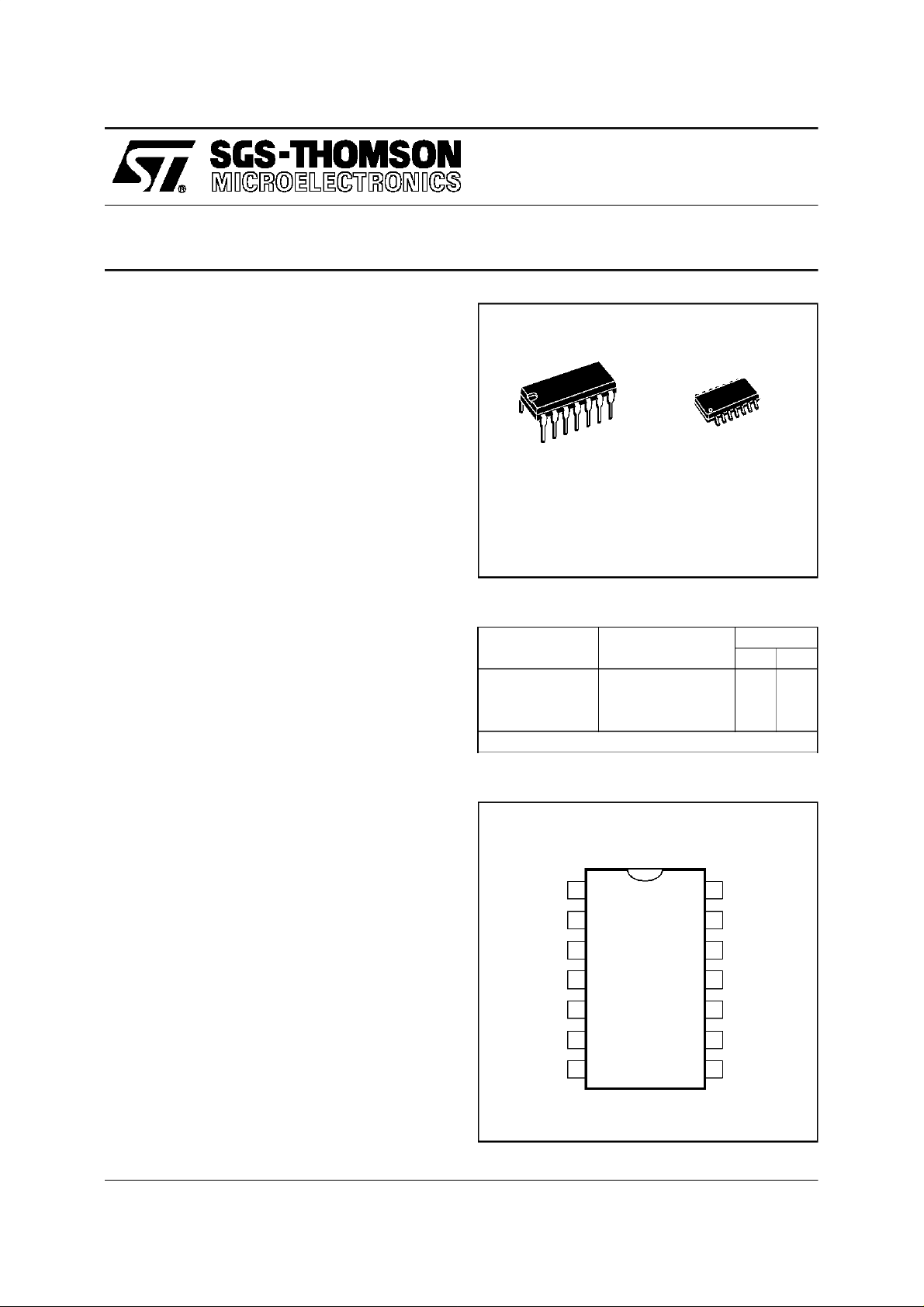
TS556C,I,M
LOW POWER DUALCMOS TIMERS
N
DIP14
(Plastic Package)
ORDER CODES
Part Number
TS556C 0
TS556I -40, +125oC ●●
TS556M -55, +125oC ●●
Examples : TS556CD , TS556IN
(Plastic Micropackage)
Temperature
Range
o
C, +70oC ●●
D
SO14
Package
ND
DESCRIPTION
TheTS556isa dualCMOStimerwhichoffersvery
low consumption(Icc
Icc
(f
Thus, eitherin Monostable or Astable mode, timing remainsvery accurate.
The TS556 provides reduced supply current
spikes during output transitions, which enables
the useof lower decouplingcapacitorscompared
to those required by bipolarNE556.
Timing capacitors can also be minimized due to
high input impedance (10
October 1997
NE556= 6mA) and high frequency
(TYP)
TS556=2.7MHz -f
(max.)
TS556= 200µA
(TYP)
(max.)
12
Ω).
NE556=0.1MHz)
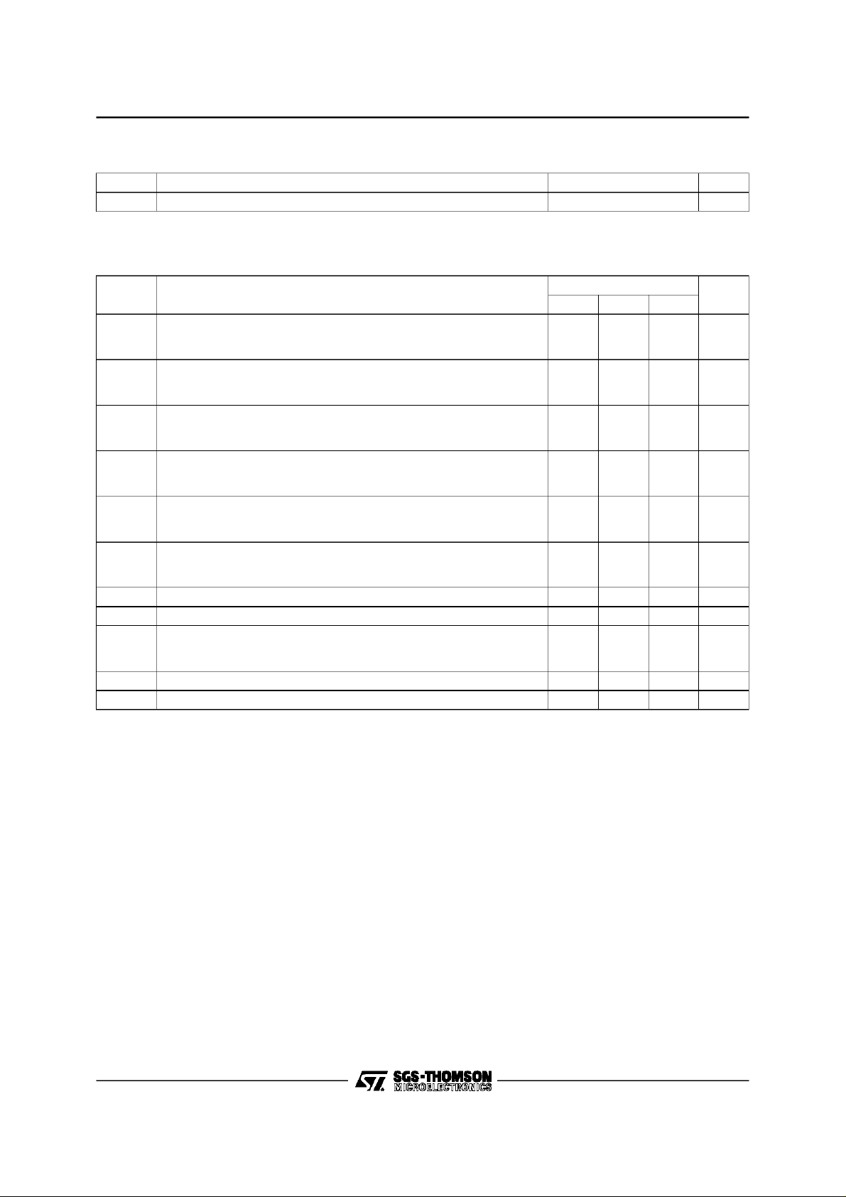
PIN CONNECTIONS (top view)
Discharge
Threshold
Control
Voltage
Reset
Output
Trigger
GND
1
2
3
4
5
6
7
14
13
12
11
10
9
8
+V
S
Discharge
Threshold
Control
Voltage
Reset
Output
Trigger
1/11

TS556C,I,M
BLOCK DIAGRAM
Threshold
Control
Voltage
Tr igger
2/12
3/11
6/8
V
CC
14
R
R
R
7
Ground
+
-
+
-
Reset
4/10
R1
Q
A
B
R
S
TS556
5/9
1/13
Output
Discharge
RESET TRIGGER THRESHOLD OUTPUT
Low x x Low
High Low x High
High High High Low
High High Low Previous State
LOW
HIGH
X
↔ Level Voltage ≤ Min voltage specified
↔ Level Voltage ≥ Max voltage specified
↔ Irrelevant
ABSOLUTEMAXIMUM RATINGS
Symbol Parameter Value Unit
V
CC
T
J
SupplyVoltage +18 V
JunctionTemperature +150
THERMALCHARACTERISTICS
Symbol Parameter Value Unit
Operating Temperature Range
TS556C
TS556I
TS556M
0 to +70
-40 to +125
-55 to +125
Storage Temperature Range -65 to +150
2/11
T
T
OPER
STG
o
C
o
C
o
C

SCHEMATIC DIAGRAM (1/2 TS556)
Τ34
TS556C,I,M
Output
Τ35
Τ33
Discharge
Τ31
Τ32
Τ29
Τ27 Τ30
Τ26
Τ25
Τ21
CC
V
Τ20
Trigger
Τ24
Τ28
Τ23
Τ17
Τ22
RESET
Τ16
GND
Τ18 Τ19
Τ15
Τ12 Τ13
Τ14
Τ11
R7
Τ10
Τ2
Threshold
Τ9
Τ7
Τ8
Τ4
Τ5 Τ6
Τ1
Ω
R1
50k
Ω
R2
50k
Control Voltage
Ω
R3
R4
50k
R5
50k Ω
50k Ω
Ω
R6
50k
3/11
TS556C,I,M
OPERATINGCONDITIONS
Symbol Parameter Value Unit
V
STATIC ELECTRICAL CHARACTERISTICS
V
CC
Symbol Parameter
I
V
V
V
V
V
I
I
V
reset
I
reset
i
Supply Voltage +2 to +16 V
CC
= +2V, T
=+25oC, Resetto VCC(unlessotherwise specified)
amb
TS556C-TS556I-TS556M
Min. Typ Max.
Supply Current (no load, High and Low States)
CC
Control Voltage
CL
Discharge Saturation Voltage (I
dis
Low Level Output Voltage (I
OL
High Level Output Voltage (I
OH
TriggerVoltage
trig
Trigger Current 10 pA
trig
Threshold Current 10 pA
TH
T
amb
T
min
T
amb
T
min
T
amb
T
min
T
amb
T
min
T
amb
T
min
T
amb
T
min
=+25oC
. ≤ T
amb
=+25oC
. ≤ T
amb
=+25oC
. ≤ T
amb
=+25oC
. ≤ T
amb
=+25oC
. ≤ T
amb
=+25oC
. ≤ T
amb
≤T
≤T
≤T
≤T
≤T
≤T
max
max
max
max
max
max
130 400
.
1.2
.
= 1mA)
dis
1.1
1.3 1.4
0.05 0.2
.
= 1mA)
sink
0.1 0.3
.
= -0.3mA)
source
.
.
1.5
1.5
0.4
0.3
1.9
0.67 0.95
Reset Voltage
T
amb
T
min
=+25oC
. ≤ T
amb
≤T
max
.
0.4
0.3
1.1 1.5
Reset Current 10 pA
Discharge Pin Leakage Current 1 100 nA
dis
400
1.5
0.25
0.35
1.05
2.0
Unit
µA
V
V
V
V
V
V
4/11

STATIC ELECTRICAL CHARACTERISTICS (continued)
= +5V, T
V
CC
Symbol Parameter
Supply Current (no load, High and Low States)
CC
Control Voltage
CL
Discharge Saturation Voltage (I
dis
Low Level Output Voltage (I
OL
High Level Output Voltage (I
OH
TriggerVoltage
trig
Trigger Current 10 pA
trig
Threshold Current 10 pA
TH
Reset Voltage
Reset Current 10 pA
Discharge Pin Leakage Current 1 100 nA
dis
V
I
V
V
V
V
V
I
I
reset
I
reset
I
=+25oC, Resetto VCC(unlessotherwise specified)
amb
=+25oC
T
amb
T
. ≤ T
≤T
≤T
≤T
≤T
≤T
≤T
≤T
max
max
max
max
max
max
max
.
.
= 10mA)
dis
.
= 8mA)
sink
.
= -2mA)
source
.
.
.
min
T
amb
T
min
T
amb
T
min
T
amb
T
min
T
amb
T
min
T
amb
T
min
T
amb
T
min
amb
=+25oC
. ≤ T
amb
=+25oC
. ≤ T
amb
=+25oC
. ≤ T
amb
=+25oC
. ≤ T
amb
=+25oC
. ≤ T
amb
=+25oC
. ≤ T
amb
TS556C,I,M
TS556C-TS556I-TS556M
Min. Typ Max.
2.9
2.8
4.4
4.4
1.36
1.26
0.4
0.3
220 500
3.3 3.8
0.2 0.3
0.3 0.6
4.6
1.67 1.96
1.1 1.5
500
3.9
0.35
0.8
2.06
2.0
Unit
µA
V
V
V
V
V
V
5/11

TS556C,I,M
STATIC ELECTRICAL CHARACTERISTICS (continued)
= +12V, T
V
CC
Symbol Parameter
Supply Current (no load, High and Low States)
CC
Control Voltage
CL
Discharge Saturation Voltage (I
dis
Low Level Output Voltage (I
OL
High Level Output Voltage (I
OH
TriggerVoltage
trig
Trigger Current 10 pA
trig
Threshold Current 10 pA
TH
Reset Voltage
Reset Current 10 pA
Discharge Pin Leakage Current 1 100 nA
dis
V
I
V
V
V
V
V
I
I
reset
I
reset
I
= +25oC, Reset to VCC(unlessotherwisespecified)
amb
=+25oC
T
amb
T
. ≤ T
≤T
≤T
≤T
≤T
≤T
≤T
≤T
max
max
max
max
max
max
max
.
.
= 80mA)
dis
.
= 50mA)
sink
.
= -10mA)
source
.
.
.
min
T
amb
T
min
T
amb
T
min
T
amb
T
min
T
amb
T
min
T
amb
T
min
T
amb
T
min
amb
=+25oC
. ≤ T
amb
=+25oC
. ≤ T
amb
=+25oC
. ≤ T
amb
=+25oC
. ≤ T
amb
=+25oC
. ≤ T
amb
=+25oC
. ≤ T
amb
TS556C-TS556I-TS556M
Min. Typ Max.
340 800
800
7.4
7.3
8 8.6
8.7
0.09 1.6
2.0
1.2 2
2.8
10.5
11
10.5
3.2
3.1
0.4
0.3
4 4.8
4.9
1.1 1.5
2.0
Unit
µA
V
V
V
V
V
V
6/11

DYNAMICELECTRICAL CHARACTERISTICS
=+25oC, Reset to VCC(unlessotherwisespecified)
T
amb
Symbol Parameter
TimingAccuracy (Monostable) - (note 1)
R = 10kΩ , C = 0.1µF
Timing Shift with supply voltage variations (Monostable)
R = 10kΩ , C = 0.1µF, V
Timing Shift with temperature
T
min.
f
max
Maximum astable frequency
= 470Ω ,RB= 200Ω, C = 200pF , VCC= + 5V 2.7
R
A
Astable frequency accuracy - (note 2)
R
A=RB
Timing Shift with supply voltage variations (Astable mode)
R
A=RB
t
Output Rise Time (VCC=+5V,C
r
Output Fall Time (VCC=+5V,C
t
f
t
t
rpw
Notes : 1. SeeFigure 2
TriggerPropagation Delay (VCC= + 5V) 100 ns
pd
Minimum Reset Pulse Width(V
2. SeeFigure 4
≤T
≤T
amb
max.,VCC
=1kΩto 100kΩ,C=0.1µF
=1kΩto 100kΩ, C = 0.1µF,VCC= 5 to+ 12V
= + 5V +/-1V 0.38
CC
=+5V
= 10pF) 25 ns
load
= 10pF) 20 - ns
load
= + 5V) 350 ns
trig
V
V
V
V
V
CC
CC
CC
CC
CC
=+5V
=+2V
=+5V
= +12V
= + 12V
TS556C,I,M
TS556C-TS556I-TS556M
Min Typ Max
1
2
4
75
3
3
0.1
Unit
%
%/V
ppm/°C
MHz
%
%/V
7/11

TS556C,I,M
TYPICALCHARACTERISTICS
Figure 1 : Supply Current (each timer) versus
SupplyVoltage
300
µ
CC
200
100
SUPPLY CURRENT, I ( A)
0481216
SUPPLY VOLTAGE, V (V)
CC
APPLICATION INFORMATION
MONOSTABLEOPERATION
In the monostable mode,the timer functions as a
one-shot. Referringto figure2 the externalcapacitor is initiallyheld dischargedby a transistor inside
the timer.
Figure2
Thecircuittriggersona negative-goinginputsignal
whenthelevelreaches1/3V
. Oncetriggered,the
CC
circuit remains in this state until the set time has
elapsed,even if it is triggered again during this
interval. The duration of the output HIGH state is
given by t = 1.1 R x C.
Noticethat sincethe chargerateand thethreshold
level of the comparator are both directly proportional to supplyvoltage, the timing intervalis independent of supply. Applying a negative pulse
simultaneouslyto the Reset terminal (pin 4 or 10)
and the Trigger terminal (pin 2 or 8) during the
timing cycledischargesthe externalcapacitorand
causesthecycletostart over.Thetimingcyclenow
starts on the positive edge of the reset pulse.
During the time the reset pulse is applied, the
output is driven to its LOWstate.
When a negative trigger pulse is applied to the
trigger terminal, the flip-flop is set, releasing the
shortcircuit acrossthe externalcapacitorand driving the output HIGH. The voltage across the capacitor increases exponentially with the time
constant τ =R xC.
Whenthe voltage across the capacitor equals 2/3
V
, thecomparatorresetsthe flip-flopwhich then
CC
discharges the capacitor rapidly and drives the
output to its LOWstate.
Figure3 showsthe actualwaveformsgeneratedin
this mode of operation.
When Reset is not used, it should be tied high to
avoid any possible or false triggering.
Trigger
8/11
V
CC
Out
Reset
1/2
TS556
R
C
Control Voltage
µ
0.01 F
Figure3
t = 0.1 ms / div
INPUT = 2.0V/div
OUTPUT VOLTAGE = 5.0V/div
CAPACITOR VOLTAGE = 2.0V/div
Ω
R = 9.1k , C= 0.01 F , R = 1.0k
µ
L
Ω

TS556C,I,M
ASTABLEOPERATION
When the circuitis connectedas shown in figure 4
it triggersitselfandfree runsas amultivibrator.The
externalcapacitor chargesthrough R
discharges through R
only. Thus the duty cycle
B
andRBand
A
may be precisely set by the ratio of these two
resistors.
In the astable mode of operation, C charges and
dischargesbetween1/3 V
and2/3 VCC.Asinthe
CC
triggered mode, the charge and discharge times
and therefore frequency, are independent of the
supplyvoltage.
Figure5 shows actualwaveformsgeneratedinthis
Figure4
V
CC
Reset
R
A
Out
mode of operation.
The charge time (output HIGH) is given by :
t1 = 0.693 (R
A+RB
)C
and the discharge time (outputLOW) by :
t2 = 0.693 (R
B
)C
Thus the total period T is given by :
T = t1 + t2 =0.693 (R
+2RB)C
A
The frequencyof oscillationis then :
1
f =
T
The duty cycle is given by : D =
=
(R
A
1.44
+ 2RB)C
R
B
RA+ 2R
B
Figure5
t = 0.5ms / div
OUTPUTVOLTAGE = 5.0V/div
Control
Voltage
µ
0.01 F
1/2
TS556
R
B
C
CAPACITOR VOLTAGE = 1.0V/div
R = R = 4.8 k , C= 0.1 F , R = 1.0k
AB
µ
L
ΩΩ
9/11

TS556C,I,M
PACKAGE MECHANICAL DATA
14 PINS- PLASTICDIP
Dimensions
Min. Typ. Max. Min. Typ. Max.
Millimeters Inches
a1 0.51 0.020
B 1.39 1.65 0.055 0.065
b 0.5 0.020
b1 0.25 0.010
D 20 0.787
E 8.5 0.335
e 2.54 0.100
e3 15.24 0.600
F 7.1 0.280
i 5.1 0.201
L 3.3 0.130
Z 1.27 2.54 0.050 0.100
PM-DIP14.EPS
DIP14.TBL
10/11

PACKAGE MECHANICAL DATA
14 PINS- PLASTICMICROPACKAGE (SO)
TS556C,I,M
Dimensions
Min. Typ. Max. Min. Typ. Max.
Millimeters Inches
A 1.75 0.069
a1 0.1 0.2 0.004 0.008
a2 1.6 0.063
b 0.35 0.46 0.014 0.018
b1 0.19 0.25 0.007 0.010
C 0.5 0.020
c1 45
o
(typ.)
D 8.55 8.75 0.336 0.334
E 5.8 6.2 0.228 0.244
e 1.27 0.050
e3 7.62 0.300
F 3.8 4.0 0.150 0.157
G 4.6 5.3 0.181 0.208
L 0.5 1.27 0.020 0.050
M 0.68 0.027
S8
Information furnished is believed tobe accurate and reliable. However, SGS-THOMSON Microelectronics assumes no responsibility
for the consequences of use of suchinformation nor for any infringement of patents or other rights of third parties which may result
from its use. No license isgranted by implication or otherwiseunder anypatent or patent rights of SGS-THOMSON Microelectronics.
Specification mentioned in this publication are subject to change without notice. This publication supersedes and replaces all
information previously supplied. SGS-THOMSON Microelectronics products are not authorized for useas critical components in life
support devices or systems withoutexpress written approval of SGS-THOMSON Microelectronics.
o
(max.)
SO14.TBL
1997 SGS-THOMSON Microelectronics – Printed in Italy – AllRights Reserved
SGS-THOMSONMicroelectronics GROUP OF COMPANIES
Australia - Brazil - Canada - China - France - Germany -Hong Kong - Italy - Japan - Korea - Malaysia - Malta - Morocco
The Netherlands - Singapore - Spain - Sweden - Switzerland - Taiwan- Thailand -United Kingdom - U.S.A.
ORDER CODE : PM-SO14.EPS
11/11
 Loading...