

QUAD OPERATIONAL AMPLIFIERS
.
LOW INPUT OFFSET VOLTAGE : 950µV max.
.
LOW VOLTAGE NOISE : 4.5nV/√√Hz
.
HIGH GAIN BANDWIDTH PRODUCT : 15M Hz
.
HIGH SLEW RATE : 7V/µµs
.
LOW DISTORTION : 0.002%
.
ESD INTERNAL PROTECTION : 2kV
DESCRIPTIO N
The TS524 is a monolithic quad operational amplifier particularly well-suited for audio applications.
The TS524 offers a very low input of fset v oltage as
well as low voltage noise (4.5nV/√Hz ) and high
dynamic performances (15MHz gain bandwidth
product, 7V/µs slew rate).
The output stage allows a large output voltage
swing and symmetrical source and sink curre nts.
PRECISIO N LO W NO ISE
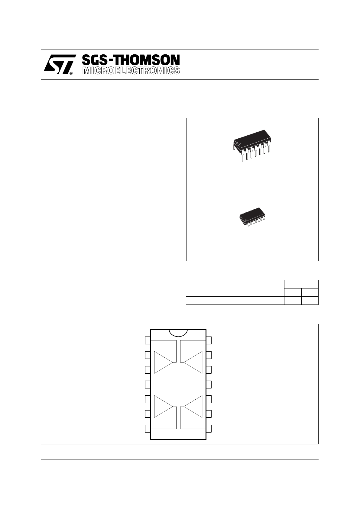
N
DIP14
(Plastic Package)
D
SO14
(Plastic Micropackage)
ORDER CODES
Part Number Temperature Range
o
TS524I -40, +125
C ••
TS524
Package
ND
PIN CONNECTIONS (top view)
Output 1
Inverting Input 1
Non-inverting Input 1
V
CC
Non-inverting Input 2
Inverting Input 2
Output 2
September 1997
14
1
2
3
+
4
5
6
7
-
+
+
-
-
+
+
-
Output 4
13
Inverting Input 4
12
Non-inverting Input 4
11
10
9
8
-
V
CC
Non-inverting Input 3
Inverting Input 3
Output 3
1/5
TS524
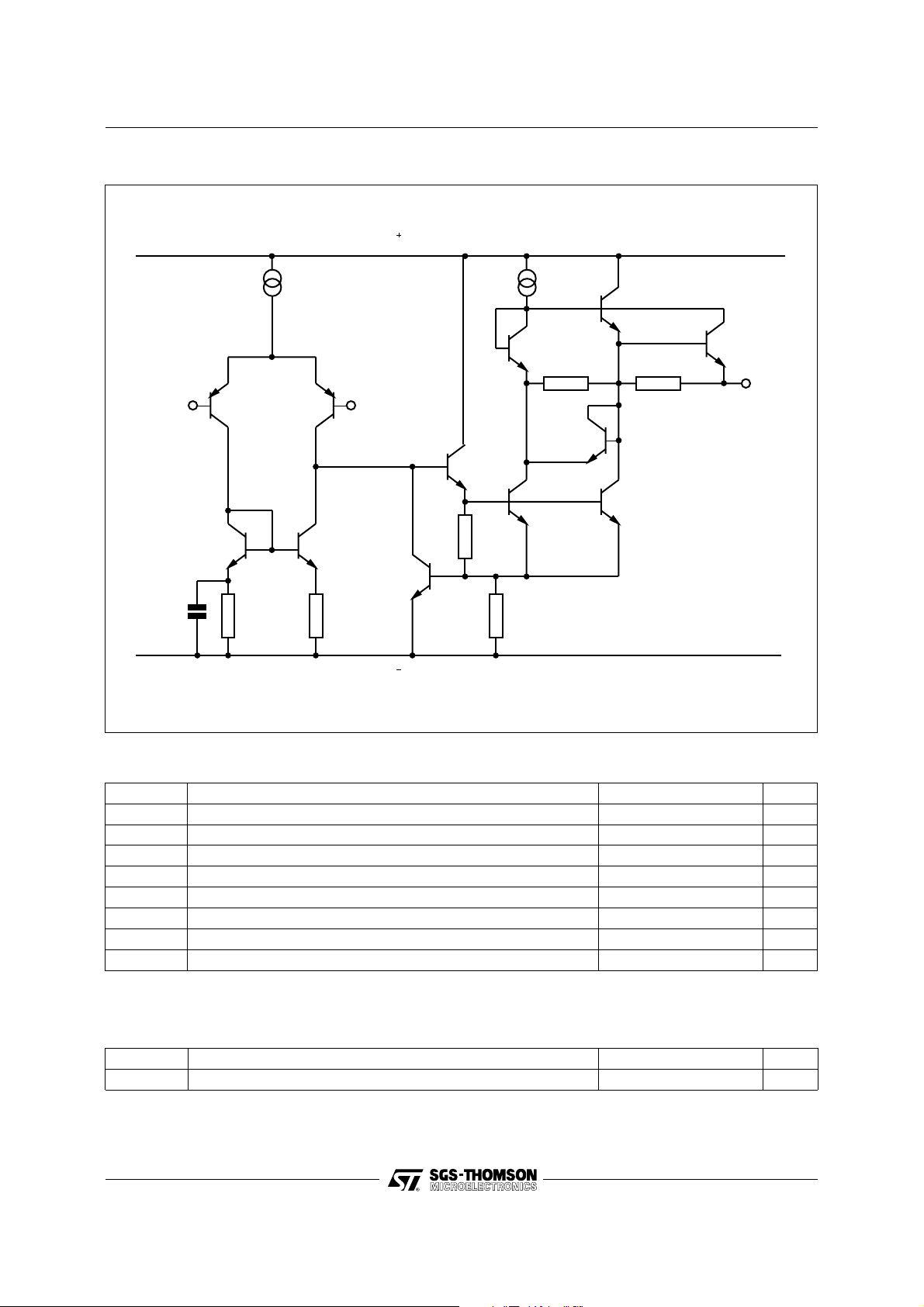
SCHEMATIC DIAGRAM (1/4 T S524)
V
CC
Inverting
Input
Non-inverting
Input
V
CC
ABSOLUTE MAXIMUM RATINGS
Symbol Parameter Value Unit
Output
V
CC
V
id
V
T
oper
T
T
stg
P
tot
Notes : 1. Either or both input voltages must not exceed the magnitude of V
Supply Voltage ±18 or +36 V
Differential Input Voltage - (note 1) ±30 V
Input Voltage - (note 1) ±15 V
i
Output Short-Circuit Duration - (note 2) Infinite
Operating Free-air Temperature Range -40 to +105
Maximum Junction Temperature +150
j
Storage Temperature -65 to +150
Maximum Power Dissipation - (note 2) 500 mW
+
-
or V
CC
2. Power dissipation must b e considered to ensure maximum junction temperature (Tj) is not exceeded
CC
o
C
o
C
o
C
OPERATING CONDITIONS
Symbol Parameter Value Unit
Supply Voltage ±2.5 to ±15 V
2/5
V
CC

ELECTRICAL CHARACTERISTICS
V
CC
+
= +15V, V
-
= -15V , T
CC
= 25oC (unless otherwise specified)
amb
Symbol Parameter Min. Typ. Max. Unit
DV
±V
V
io
I
io
I
ib
V
icm
A
vd
opp
Input Offset Voltage (Vo = 0V, Vic = 0V)
≤ T
T
min.
Input Offset Voltage Drift
io
Vic = 0V, Vo = 0V, T
Input Offset Current (V
T
amb
T
min.
Input Bias Current (V
T
amb
T
min.
amb
= +25oC
≤ T
amb
= +25oC
≤ T
amb
≤ T
≤ T
≤ T
max.
max.
ic
max.
≤ T
amb
≤ T
min.
= 0V, VO = 0V)
ic
= 0V, VO = 0V)
max.
10 150
250 750
Common Mode Input Voltage Range (∆VIO = 5mV, VO = 0V) ±13 ±14 V
Large Signal Voltage Gain (RL = 2kΩ, VO = ±10V)
T
amb
T
min.
= +25oC
≤ T
amb
≤ T
max.
90
85
100
Output Voltage Swing (Vid = ±1V)
RL = 600Ω
RL = 600Ω
12.2
-12.7
0.95
1.8
2
175
800
TS524
mV
µV/oC
nA
nA
dB
V
CMR Common Mode Rejection Ratio (V
SVR Supply Voltage Rejection Ratio
I
o
+
V
CC
-
/ V
= +15V / -15V to +5V / -5V 80 105
CC
Output Short Circuit Current (Vid = ±1V, Output to Ground)
Source
Sink
I
CC
Supply current (VO = 0V, All Amplifiers)
= +25oC
T
amb
T
≤ T
amb
≤ T
max.
min.
= 2.0kΩ
R
L
RL = 2.0kΩ
= 10kΩ
R
L
RL = 10kΩ
= ±13V) 80 100 dB
ic
13.2
13.5
15
20
14
-14.2
-13.2
14.3
-14.6
-14
29
37
810
12
SR Slew Rate
V
= -10V to +10V, RL = 2kΩ, CL = 100pF, AV = +1 5 7
i
GBP Gain Bandwidth Product (f = 100kHz, R
= 2kΩ, CL = 100pF) 10 15 MHz
L
B Unity Gain Bandwidth (Open loop) 9 MHz
A
m
Gain Margin (RL = 2kΩ)C
∅m Phase Margin (R
e
n
i
n
Equivalent Input Noise Voltage (RS = 100Ω, f = 1kHz) 4.5
Equivalent Input Noise current (f = 1kHz) 0.5
= 0pF
L
= 100pF
C
L
= 2kΩ)C
L
= 0pF
L
CL = 100pF
-11
-6
55
30
THD Total Harmonic Distortion
RL = 2kΩ, f = 20Hz to 20kHz, VO = 3V
V
O1/VO2
Channel Separation (f = 20Hz to 20kHz) 120 dB
FPB Full Power Bandwidth (V
Z
o
R
C
Output Impedance (VO = 0V, f = 9MHz) 37 Ω
Input Resistance (Vic = 0V) 175 kΩ
i
Input Capacitance (Vic = 0V) 12 pF
i
= 27Vpp, RL = 2kΩ, THD ≤ 1%) 120 kHz
O
, AV = +1 0.002
rms
dB
mA
mA
V/µs
dB
Degrees
nV
Hz
√
pA
Hz
√
%
3/5

TS524
PACKAGE MECHANICAL DATA
14 PINS - PLASTIC DIP
Dimensions
Min. Typ. Max. Min. Typ. Max.
Millimeters Inches
a1 0.51 0.020
B 1.39 1.65 0.055 0.065
b 0.5 0.020
b1 0.25 0.010
D 20 0.787
E 8.5 0.335
e 2.54 0.100
e3 15.24 0.600
F 7.1 0.280
i 5.1 0.201
L 3.3 0.130
Z 1.27 2.54 0.050 0.100
PM-DIP14.EPS
DIP14.TBL
4/5

PACKAGE MECHANICAL DATA
14 PINS - PLASTIC MICROPACKAGE (SO)
TS524
Dimensions
Min. Typ. Max. Min. Typ. Max.
Millimeters Inches
A 1.75 0.069
a1 0.1 0.2 0.004 0.008
a2 1.6 0.063
b 0.35 0.46 0.014 0.018
b1 0.19 0.25 0.007 0.010
C 0.5 0.020
c1 45
o
(typ.)
D 8.55 8.75 0.336 0.334
E 5.8 6.2 0.228 0.244
e 1.27 0.050
e3 7.62 0.300
F 3.8 4.0 0.150 0.157
G 4.6 5.3 0.181 0.208
L 0.5 1.27 0.020 0.050
M 0.68 0.027
S8
Information furnished i s believed to be accurate and rel iabl e. However, S GS-THOMSON Microel ectroni cs assumes no responsibil ity
for the consequences of use of such information nor for any infringement of patents or other rights of third parties which may result
from its use. No license is granted by implication or otherwise under any patent or patent rights of SGS-THOMSON Microelectronics.
Specification mentioned in this publication are subject to change without notice. This publication supersedes and replaces all
information previously supplied. SGS-THOMSON Microelectronics products are not authorized for use as critical components in life
support devices or systems without express written approval of SGS-THOMSON Microelectronics.
o
(max.)
SO14.TBL
© 1997 SGS-THOMSON Microelectronics – Printed in Italy – All Rights Reserved
SGS-THOMSON Microelectronics GROUP OF COMPANIES
Australia - Brazil - Canada - China - France - Germany - Hong Kong - Italy - Japan - Korea - Malaysia - Malta - Morocco
The Netherlands - Singapore - Spain - Sweden - Switzerland - Taiwan - Thailand - United Kingdom - U.S.A.
ORDER CODE : PM-SO14.EPS
5/5
 Loading...