

Datasheet TS5070, TS5071N, TS5071, TS5070FN, TS5070FNTR Datasheet (SGS Thomson Microelectronics)
PROGRAMMABLE CODEC/FILTER
COMPLETE CODEC AND FILTER SYSTEM
INCLUDING:
– TRANSMIT ANDRECEIVE PCM CHANNEL
FILTERS
– µ-LAW OR A-LAW COMPANDING CODER
AND DECODER
– RECEIVE POWER AMPLIFIER DRIVES
300 Ω
– 4.096 MHz SERIAL PCM DATA(max)
PROGRAMMABLE FUNCTIONS :
– TRANSMIT GAIN : 25.4 dB RANGE, 0.1 dB
STEPS
– RECEIVE GAIN : 25.4 dB RANGE, 0.1 dB
STEPS
– HYBRID BALANCE CANCELLATION FIL-
TER
– TIME-SLOT ASSIGNMENT: UP TO 64
SLOTS/FRAME
– 2 PORTASSIGNMENT (TS5070)
– 6 INTERFACELATCHES (TS5070)
–AORµ-LAW
– ANALOG LOOPBACK
– DIGITAL LOOPBACK
DIRECT INTERFACE TO SOLID-STATE
SLICs
SIMPLIFIES TRANSFORMER SLIC, SINGLE
WINDINGSECONDARY
STANDARDSERIALCONTROL INTERFACE
80 mW OPERATINGPOWER (typ)
1.5mWSTANDBYPOWER(typ)
MEETS OR EXCEEDS ALL CCITT AND
LSSGRSPECIFICATIONS
TTL AND CMOS COMPATIBLE DIGITAL IN-
TERFACES
DESCRIPTION
TheTS5070seriesarethesecondgenerationcombined PCM CODEC and Filter devices optimized
for digital switching applicationson subscriberand
trunk line cards.
Usingadvancedswitchedcapacitortechniquesthe
TS5070 and TS5071 combine transmit bandpass
and receive lowpass channel filters with a companding PCM encoder and decoder. The devices
are A-lawand µ-law selectableand employ a conventional serial PCM interface capable of being
clockedup to 4.096MHz.A numberofprogrammable functionsmay be controlled via a serial control
port.
TS5070
TS5071
COMBO 2
ORDERING NUMBER:TS5071N
ORDERING NUMBERS: TS5070FN
Channel gains are programmableover a 25.4 dB
range in each direction, and a programmablefilter
is included to enable Hybrid Balancing to be adjustedto suit a wide range of loop impedanceconditions.
Both transformerand activeSLIC interfacecircuits
with real or complex termination impedances can
be balanced by this filter, with cancellation in excessof 30 dBbeingreadilyachievablewhenmeasuredacrossthepassbandagainststandardtesttermination networks.
ToenableCOMBOIIG to interfaceto theSLICcontrol leads, a number of programmable latches are
included; each may be configuredas eitheran input or an output. The TS5070 provides 6 latches
and the TS5071 5 latches.
ND GENERATION
DIP20 (Plastic)
PLCC28
TS5070FNTR
December 1997
1/32
TS5070 - TS5071
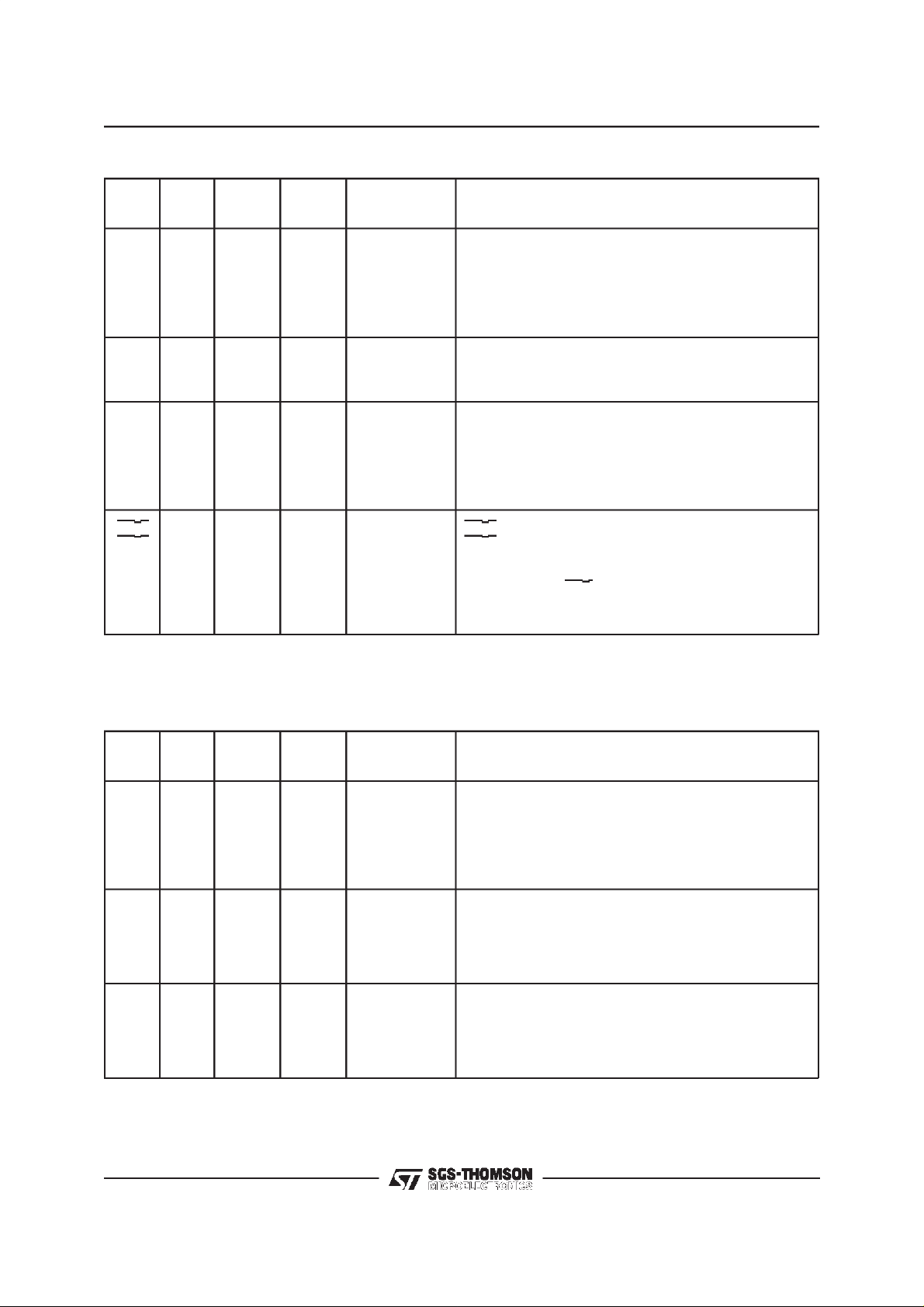
TS5070 PIN FUNCTIONALITY (PLCC28)
No. Name Function
1 GND Ground Input(+0V)
2VF
3V
4 NC Not Connected
5 NC Not Connected
6 IL3 Digital Input or Outputdefined by LDR register content
7 IL2 Digital Input or Outputdefined by LDR register content
8FS
9D
10 D
11 CO Digital output (shiftedout on CCLK rising edge)
12 CI Digital input (sampled on CCLK falling edge)
13 CCLK Digital input (clock)
14 CS Digital input (chip select forCI/CO)
15 MR Digital Input
16 BCLK Digital input (clock)
17 MCLK Digital input
18 D
19 D
20 TS
21 TS
22 FS
23 IL5 Digital input or output defined by LDR register content
24 IL4 Digital input or output defined by LDR register content
25 IL1 Digital input or output defined by LDR register content
26 IL0 Digital input or output defined by LDR register content
27 V
28 VF
0 Analog Output
R
SS
R
1 Digital input sampled by BCLK falling edge
R
0 Digital input sampled by BCLK falling edge
R
0 Digital output clocked by BCLK rising edge
X
1 Digital output clocked by BCLK rising edge
X
X
X
X
CC
X
Supply Input(-5V)
Digital input
0 Open drain output (pulled low by active DX0 time slot)
1 Open drain output (pulled low by active DX1 time slot)
Digital input
Supply input (+5V)
I Analog input
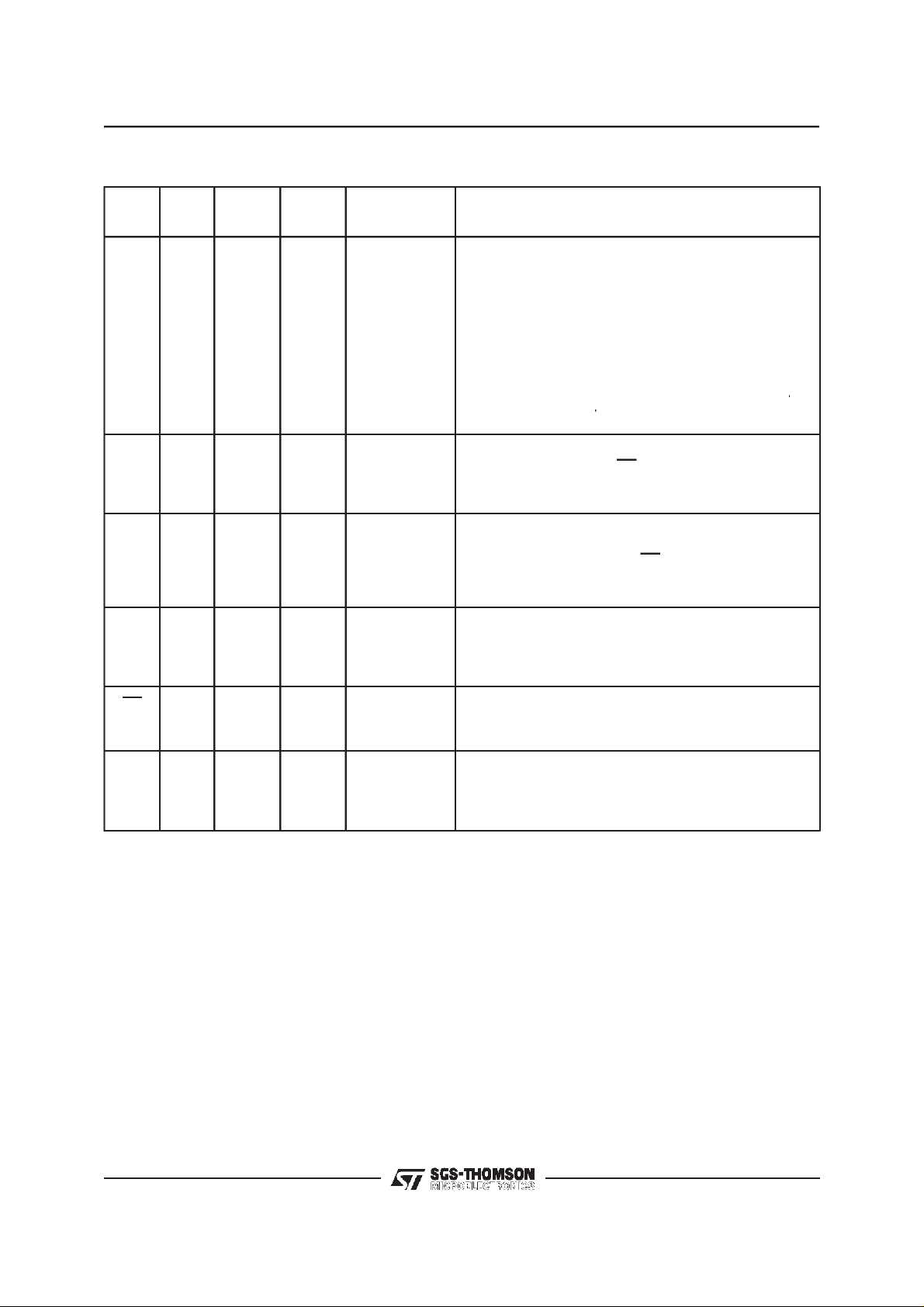
TS5070 FUNCTIONALDIAGRAM
VFXI
HYBAL 1
HYBAL 2
HYBAL 3
VFRO
GND
IL5
IL4
IL3
IL2
IL1
IL0
TS5070/71
INTERFACE
LATCHES
TX GAIN
HYBRID
BALANCE
FILTER
RX GAIN
LATCH DIR
LATCH CONT.
VSS=-5VVCC=+5V
Vref
TX TIME SLOT
CTL REG.
RX TIME SLOT
ENCODER
REGISTER
TIME-SLOT
ASSIGNMENT
REGISTER
DECODER
CONTROL
INTERFACE
D94TL135
TX
RX
AZ
DX0
DX1
TSX0
TSX1
FSX
BCLK
FSR
DR0
DR1
MCLK
MR
CS
CCLK
CO
CI
2/32
BLOCK DIAGRAM
TS5070 - TS5071
ABSOLUTE MAXIMUM RATINGS
Symbol Parameter Value Unit
V
V
V
I
T
T
lead
VCCto GND 7 V
CC
VSSto GND – 7 V
SS
Voltage at VFXI V
Voltage at Any Digital Input VCC+ 0.5 to GND – 0.5 V
IN
+ 0.5 to VSS– 0.5 V
CC
Current at VFRO ± 100 mA
Current at Any DigitalOutput ± 50 mA
O
Storage Temperature Range – 65, + 150 °C
stg
Lead Temperature Range (soldering, 10 seconds) 300 °C
3/32
TS5070 - TS5071
PIN CONNECTIONS
PLCC28
TS5070FN
DIP20
TS5071N
POWERSUPPLY, CLOCK
Name
V
CC
V
GND
BCLK I 16 12 Bit Clock Bit clockinput used to shift PCM data into and out of the
MCLK I 17 12 Master Clock Master clock input used by the switched capacitor filters
Pin
Type
SS
TS5070FNTS5071
S
S
S
27
N
19
3
1
3
1
Function Description
Positive Power
Supply
Negative
Power Supply
Ground
+5V±5%
–5V±5%
All analog and digital signals are referenced to this pin.
and DXpins. BCLK may vary from 64 kHz to 4.096
D
R
MHz in 8 kHz increments, andmust be synchronous with
MCLK (TS5071 only).
and the encoder and decoder sequencing logic. Must be
512 kHz, 1. 536/1. 544 MHz,
2.048 MHz or 4.096 MHz and synchronous with BCLK.
BCLK and MCLK arewired together in the TS5071.
4/32
TRANSMITSECTION
TS5070 - TS5071
Name
FS
VF
D
D
TS
TS
Pin
Type
X
I I 28 20 Transmit
X
0
X
1
X
0
X
1
X
TS5070FNTS5071
N
I 22 15 Transmit
0
0
0
0
18
19
20
21
13
–
14
–
Function Description
Normally apulse or squarewave waveform with an 8 kHz
Frame Sync.
repetition rate is applied to this input to definethe startof
the transmit time-slot assigned to this device (non-delayed
data mode) or the start of the transmit frame (delayed
data mode using the internal time-slot assignment
counter).
This is a high–impedance input. Voice frequency signals
Analog
present on this input are encoded as an A–law or µ–law
PCM bit stream and shifted out on the selected D
Transmit Data D
1 is available on the TS5070 only, DX0 is available on
X
all devices. These transmit data TRI–STATEoutputs
remain in the high impedance state except during the
assigned transmit time–slot on the assigned port, during
which the transmit PCM data byte is shifted out on the
rising edges of BCLK.
Transmit
Time–slot
1 is available on the TS5070 only.
TS
X
TS
0 is available on all devices. Normally these opendrain
X
outputs are floating in a high impedance state except
when a time–slot is activeon one of the D
the apppropriate TS
output pulls low to
X
enable a backplane line–driver. Should be strapped to
ground (GND) when not used.
pin.
X
outputs, when
X
RECEIVESECTION
Name
FS
VF
D
D
Pin
Type
R
0 0 2 2 Receive Analog The receive analog power amplifier output, capable of
R
0
R
1
R
TS5070FNTS5071
N
Function Description
I 8 6 Receive Frame
Sync.
I
I
10
7
9
Receive Data D
–
Normally apulse or squarewave waveform with an 8 kHz
repetition rate is applied to this input to definethe startof
the receive time–slot assigned to this device (non-delayed
frame mode) or the startof the receive frame (delayed
frame mode using the internal time-slot assignment
counter.
driving load impedances as low as 300Ω(depending on
the peak overload levelrequired). PCM data received on
the assigned D
pin is decoded and appears at this output
R
as voice frequency signals.
1 is availableon the TS5070 only, DR0 isavailable on
R
all devices. These receive data input(s) are inactive
except during the assigned receive time–slot of the
assigned port when the receive PCM data is shifted inon
the falling edges of BCLK.
5/32
TS5070 - TS5071
INTERFACE, CONTROL, RESET
Name
IL5
IL4
IL3
IL2
IL1
IL0
CCLK I 13 9 Control Clock This clock shifts serial control information into or out of CI
CI/O I/O – 8 Control Data
CI
CO
Pin
Type
TS5070FNTS5071
I/O
I/O
I/O
I/O
I/O
I/O
I
O
23
24
25
26
12
11
N
–
16
6
7
4
5
17
18
–
–
Function Description
Interface
Latches
Input/output
Control Data
Input
Control Data
Output
IL5 throughIL0 are available on the TS5070,
IL4 throughIL0 are available on the TS5071.
Each interfaceLatch I/O pin may be individually
programmed as an input or an output determined by the
state of the corresponding bit in the Latch Direction
Register (LDR) . For pins configured as inputs, thelogic
state sensed on each input is latched into the interface
Latch Register (ILR) whenever control data is written to
COMBO IIG, while CS is low, and the information is
shifted out on the CO (or CI/O) pin. Whenconfigured as
outputs, control data written into the ILR appears at the
corresponding IL pins.
or CO (or CI/O) when the CS input is low depending on
the currentinstruction. CCLK may be asynchronous with
the othersystem clocks.
This is Control Data I/O pin wich is provided on the
TS5071. Serial control information is shifted into orout of
COMBO IIG on this pinwhen CS is low. The directionof
the datais determined by the current instruction as defined
in Table 1.
These are separate controls, availables only on the
TS5070. They can be wired together if required.
CS I 14 10 Chip Select When this pins is low, control information can be written to
MR I 15 11 Master Reset This logicinput must be pulled lowfor normal operation of
FUNCTIONAL DESCRIPTION
POWER-ONINITIALIZATION
When power is first applied, power-on reset cir-
cuitry initializes COMBO IIG and puts it into the
power-down state. The gain control registers for
the transmit and receive gain sections are programmed for no output, the hybrid balance circuit
is turned off, the power amp is disabled and the
device is in the non-delayed timing mode. The
Latch Direction Register (LDR) is pre-set with all
IL pins programmed as inputs, placing the SLIC
interface pins in a high impedance state. The
or readfrom the COMBO IIG via the CI and CO pins (or
CI/O).
COMBO IIG. When pulled momentarily high, all
programmable registers in the device are resetto the
states specified under ”Power–on Initialization”.
CI/O pin is set as an input ready for the first control byte of the initializationsequence.Other initial
states in the Control Register are indicated in Table 2.
Aresetto thesesameinitialconditionsmayalsobe
forcedby drivingtheMR pinmomentarilyhigh. This
maybedone eitherwhenpowered-upor down.For
normaloperationthispin must be pulledlow. If not
used,MR shouldbe hard-wired to ground.
The desired modesforall programmablefunctions
may be initialized via the control port prior to a
Power-upcommand.
6/32

TS5070 - TS5071
POWER-DOWN STATE
Following a period of activity in the powered-up
state the power-down state may be re-entered by
writing any of the control instructionsinto the serial
control port with the ”P” bit set to ”1” It is recommendedthat thechipbepowereddownbefore writing any additional instructions. In the power-down
state, all non-essential circuitry is de-activated and
0andDX1outputsarein the highimpedance
theD
X
TRI-STATEcondition.
Thecoefficientsstoredin theHybridBalancecircuit
and the Gain Controlregisters,the data in the LDR
and ILR, and all control bits remain unchanged in
the power-down state unless changed by writing
new data via the serialcontrolport,whichremains
operational. The outputs of the Interface Latches
also remainactive, maintaining the ability to monitor and control a SLIC.
TRANSMITFILTERAND ENCODER
The Transmitsection input, VF
I, is a high imped-
X
ance summinginputwhichis usedas thedifferencingpointfortheinternalhybridbalancecancellation
signal. No external componentsare needed to set
the gain. Following this circuit is a programmable
gain/attenuationamplifierwhichiscontrolledbythe
contents of the Transmit Gain Register (see Programmable Functions section). An active prefilter
then precedesthe 3rd order high-pass and 5th order low-pass switched capacitor filters. The A/D
converterhas acompressingcharacteristicaccording to the standard CCITT A orµ255 coding laws,
whichmustbe selectedbya controlinstructionduring initialization(see table 1 and 2). A precisiononchipvoltagereferenceensuresaccurateand highly
stable transmissionlevels. Any offset voltage arising in the gain-set amplifier, the filters or the comparatoris cancelledbyaninternalauto-zerocircuit.
Each encode cycle begins immediately following
the assigned Transmit time-slot. The total signal
delay referencedto the start of thetime-slot is approximately 165µs (due to the Transmit Filter)
plus 125 µs (due to encoding delay), which totals
290 µs. Data is shifted out on D
0orDX1 during
X
the selected time slot on eight rising edges of
BCLK.
Register,isincluded,andfinallyaPost-Filter/Power
Amplifier capable of driving a 300Ωload to±3.5
V, a 600 Ω load to ± 3.8 Vor 15 kΩ loadto ± 4.0 V
at peakoverload.
A decode cycle begins immediately after each receive time-slot, and 10µs later the Decoder DAC
output is updated. The total signal delay is 10µs
plus 120 µs (filter delay) plus 62.5 µs (1/2 frame)
whichgives approximately190 µs.
PCM INTERFACE
TheFS
and FSRframe syncinputsdeterminethe
X
beginning of the 8-bit transmit and receive timeslots respectively. They may have any duration
from a single cycle of BCLK to one MCLK period
LOW. Two different relationships may be establishedbetweentheframesyncinputsandtheactual
time-slotson thePCMbussesby settingbit 3 inthe
Control Register (see table 2). Non delayed data
mode is similar to long-frame timing on the
ETC5050/60 series of devices : time-slots being
nominallycoincident with the rising edge ofthe appropriate FS input. The alternative is to use Delayed Data mode which is similar to short-frame
sync timing, in which each FS input must be high
at least a half-cycleof BCLK earlier than the timeslot.
TheTime-SlotAssignmentcircuit onthedevicecan
onlybeusedwithDelayedDatatiming.Whenusing
Time-Slot Assignment, the beginning of the first
time-slot in a frameis identified by the appropriate
FSinput.Theactualtransmitandreceivetime-slots
are then determined by the internalTime-Slot Assignment counters. Transmit and Receive frames
and time-slots may be skewedfrom each other by
any number of BCLK cycles.
During each assigned transmit time-slot, the selected D
register on the rising edges of BCLK. TS
TS
0/1 output shifts data out from the PCM
X
1 as appropriate)also pulls low for the first 7
X
0 (or
X
1/2 bit times of the time-slot to control the TRISTATE Enable of a backplane line driver. Serial
PCM data is shifted into the selected D
0/1 input
R
during each assigned Receive time slot on the
falling edges of BCLK. D
1 are selectableon the TS5070 only.
D
R
0orDX1 and DR0or
X
DECODERAND RECEIVE FILTER
PCM data is shifted into the Decoder’s Receive
PCMRegistervia theD
0orDR1pinduringthe se-
R
lectedtime-slotonthe8fallingedgesofBCLK.The
Decoder consistsof an expandingDAC with either
Aorµ255law decodingcharacteristic, which is selectedby thesamecontrolinstructionusedtoselect
the Encode law during initialization. Following the
Decoderisa 5thorder low-passswitched capacitor
filter with integral Sin x/x correction for the 8 kHz
sample and hold. A programmablegain amplifier,
which must be set by writing to the Receive Gain
SERIALCONTROL PORT
Control information and data are written into or
readback from COMBO IIG via the serial control
portconsistingof the controlclockCCLK; theserial
data input/output CI/O (or separate input CI, and
output CO on the TS5070only); and the ChipSelect input CS. All control instructions require 2
bytes,as listedintable1, withtheexceptionof asingle bytepower-up/downcommand. Thebyte1bits
are used as follows: bit 7 specifies power-up or
power-down;bits 6, 5, 4 and 3 specifythe register
address; bit 2 specifies whetherthe instructions is
read or write; bit 1 specifies a one or two byte in-
7/32

TS5070 - TS5071
struction;and bit0 is not used.Toshiftcontroldata
into COMBO IIG, CCLK must be pulsed high 8
timeswhile CS is low. DataontheCI or CI/Oinput
is shifted into the serial input registeron the falling
edge of each CCLK pulse. After all data is shifted
in, the contentsof the input shift register are decoded, and may indicate that a 2nd byte of control
data willfollow.Thissecondbyte mayeitherbe definedby asecondbyte-wideCSpulseormayfollow
the firstcontinuously,i.e. it isnotmandatoryfor CS
to returnhigh in betweenthe first and secondcontrol bytes.Onthefalling edgeofthe8
th
CCLKclock
pulse in the 2nd controlbytethedataisloadedinto
theappropriateprogrammableregister.CSmayremain low continuouslywhen programmingsucces-
siveregisters,ifdesired.HoweverCS shouldbe set
high when no data transfersare in progress.
ToreadbackinterfaceLatch dataor statusinformationfromCOMBOIIG,thefirstbyteofthe appropriateinstructionisstrobedinduringthe firstCSpulse,
asdefinedin table1.CS must thenbetakenlowfor
a further 8 CCLK cycles, during which the data is
shiftedontotheCO or CI/O pin on therisingedges
of CCLK. When CS ishighthe CO or CI/Opin is in
thehigh-impedanceTRI-STATE,enablingtheCI/O
pins of many devices to be multiplexed together.
Thus, to summarize, 2-byte READ and WRITE instructionsmay use eithertwo 8-bit wideCSpulses
or a single 16-bit wide CS pulse.
Table 1: ProgrammableRegister Instructions
Function
76543210
Single Byte Power–up/down PXXXXX0X None
Write Control Register
Read–back Control Register
Write Latch Direction Register (LDR)
Read Latch Direction Register
Write Latch Content Register (ILR)
Read Latch Content Register
Write Transmit Time–slot/port
Read–back Transmit Time–slot/port
Write Receive Time–slot/port
Read–back Receive Time–slot/port
Write Transmit Gain Register
Read Transmit Gain Register
Write Receive Gain Register
Read Receive Gain Register
Write Hybrid Balance Register ≠ 1
Read Hybrid Balance Register ≠ 1
Write Hybrid Balance Register≠2
Read Hybrid Balance Register ≠ 2
Write Hybrid Balance Register ≠ 3
Read Hybrid Balance Register≠3
PP000000000111X
PP000011000111X
PP000000110111X
PP110011000111X
PP110000110111X
PP001100110111X
PP001100000111X
PP001111000111X
PP001111110111X
PP110000000111X
Byte 1
X
X
X
X
X
X
X
X
X
X
See Table 2
See Table 2
See Table 4
See Table 4
See Table 5
See Table 5
See Table 6
See Table 6
See Table 6
See Table 6
See Table 7
See Table 7
See Table 8
See Table 8
See Table 9
See Table 9
See Table 10
See Table 10
Byte 2
Notes: 1. Bit 7 of bytes 1 and 2 is always the first bit clocked into or out of the CI, CO or CI/CO pin.
PROGRAMMABLE FUNCTIONS
POWER-UP/DOWN CONTROL
Following power-on initialization, power-up and
power-down control may be accomplished by
writing any of the control instructions listed in table 1 into COMBO IIG with the ”P” bit set to ”0”
for power-up or ”1” for power-down. Normally it is
recommendedthat all programmable functions be
initially programmed while the device is powered
down. Power state control can then be included
with the last programming instruction or the sepa-
8/32
2. ”P” is the power-up/down control bit, see ”Power-up” section (”0” = Power Up ”1” = Power Down).
rate single-byte instruction. Any of the programmable registers may also be modified while the
device is powered-up or down be setting the ”P”
bit as indicated.When the power up or down control is entered as a single byte instruction, bit one
(1) must be set to a 0.
When a power-up command is given, all de-activated circuits are activated, but the TRI-STATE
PCM output(s), D
0 (and DX1), will remain in the
X
high impedance state until the second FS
after power-up.
X
pulse
TS5070 - TS5071
CONTROLREGISTERINSTRUCTION
The first byte of a READ or WRITE instruction to
the Control Register is as shown in table 1. The
second byte functionsare detailed in table 2.
MASTER CLOCKFREQUENCY SELECTION
A Master clock must be provided to COMBO IIG
for operation of the filter and coding/decoding
functions. The MCLK frequency must be either
512 kHz, 1.536 MHz, 1.544 MHz, 2.048 MHz, or
4.096 MHz and must be synchronouswith BCLK.
Bits F1 and F0 (see table 2) must be set during
initializationto selectthe correctinternal divider.
ANALOGLOOPBACK
Analog Loopback mode is entered by setting the
”AL”and”DL” bits in theControl Registeras shown
in table2. In the analogloopbackmode,theTransmit input VF
ternally connected to the VF
loop from the Receive PCM Register back to the
TransmitPCM Register.The VF
tive, and the programmed settings of the Transmit
and Receive gains remain unchanged, thus care
must be taken to ensure that overload levels are
notexceededanywherein theloop.
Hybrid balancing must be disabled for meaning
ful analogloopbackFunction.
CODINGLAW SELECTION
Bits ”MA” and ”IA” in table 2 permit the selection
of µ255 coding or A-law coding with or without
even-bit inversion.
DIGITALLOOPBACK
Digital Loopback mode is entered by setting the
”DL”bitintheControlRegisterasshownintable2.
Table 2: ControlRegister Byte 2 Functions
Bit Number
76543210
F1 F0 MA IA DN DL AL PP
0
0
1
1
0
1
0
1
0
1
1
X
0
1
0
1
0
1
0
0
X
1
I is isolatedfromthe inputpin and in-
X
Function
MCLK = 512kHz
MCLK = 1.536 or 1. 544 MHz
MCLK = 2.048 MHz
MCLK = 4.096 MHz
Select µ. 255 Law
A–law, Including Even Bit Inversion
A–Law, No Even Bit Inversion
Delayed Data Timing
Non–delayed Data Timing
Normal Operation
Digital Loopback
Analog Loopback
0
Power Amp Enabled in PDN
1
Power Amp Disabled in PDN
*
*
O output, forming a
R
O pin remainsac-
R
*
*
*
(*) State at power-on initialization (bit 4 = 0)
Table 3: Coding Law Conventions.
m255 Law
MSB LSB
V
= +Full Scale 100000001010101011111111
IN
=0V 10111111111111111011001100110011100000000000000
V
IN
V
= -Full Scale 000000000010101001111111
IN
Note: The MSB is always the first PCM bitshifted in or out ofCOMBO IIG.
True A-law with
even bit inversion
MSB LSB
A-law without
even bit inversion
MSB LSB
0
9/32
TS5070 - TS5071
This mode provides another stage of path verificationby enablingdata written into the ReceivePCM
Register to be read back from that register in any
Transmittime-slotat D
0orDX1.
X
For Analog Loopback as well as for Digital Loopback PCM decoding continues and analog output
appears at VF
O. The output can be disabled by
R
pro gramming ”No Output” in the Receive Gain
Register (see table 8).
INTERFACELATCHDIRECTIONS
Immediately following power-on, all Interface
Latches assume they are inputs, and therefore all
IL pins are in a high impedance state. Each IL pin
maybe individuallyprogrammedasa logicinputor
output by writing the appropriateinstructionto the
LDR, see table 1 and 4. Bits L
must be set by
5-L0
writing the specific instruction to the LDR with the
L bits in thesecondbyte setasspecifiedin table4.
Unused interface latches should be programmed
as outputs.For the TS5071, L5 should always be
programmedas an output.
Table4: Byte2 Functionof LatchDirection Register
Bit Number
76543210
L0 L1 L2 L3 L4 L5 X X
LNBit IL Direction
0
1
(*) State atpower-on initilization.
Note: L5 should be programmed as an output for the TS5071.
Input
Output
*
INTERFACE LATCH STATES
Interface Latches configured as outputs assume
the state determinedby theappropriate data bit in
the 2-byte instruction written to the Latch Content
Register (ILR) as shown in tables 1 and 5.
Latches configured as inputs will sense the state
applied by an external source, such as the OffHook detect output of a SLIC. All bits of the ILR,
i.e. sensed inputs and the programmed state of
outputs, can be read back in the 2nd byte of a
READ from the ILR. It is recommended that, during initialization, the state of IL pins to be configured as outputs should first be programmed, followed immediately by the Latch Direction
Register.
Table 5: Interface LatchData Bit Order
Bit Number
76543210
D0 D1 D2 D3 D4 D5 X X
TIME-SLOTASSIGNMENT
COMBOIIGcan operatein eitherfixedtime-slotor
time-slotassignmentmodeforselectingthe Transmitand ReceivePCM time-slots.Followingpoweron,the deviceis automaticallyinNon-DelayedTimingmode,in whichthe time-slotalwaysbegins with
the leading (rising) edge of frame sync inputsFS
and FSR. Time-SlotAssignment may only be used
with Delayed Data timing : see figure 6. FS
FS
may have any phase relationship with each
R
X
and
other in BCLKperiod increments.
X
Table 6: Byte 2 of Time-slotand Port Assignment Instructions
Bit Number Function
7
EN
0X X XXXXX
10
11
Notes:
1. The ”PS” bit MUST always be set to 0 for theTS5071.
2. T5 is the MSB of thetime-slot assignment.
(*) State at power-on initialization
10/32
6
PS
(note 1)
5
T5
(note 2)
Assign One Binary CodedTime-slot from0–63
Assign One Binary CodedTime-slot from0–63
Assign One Binary CodedTime-slot from0–63
Assign One Binary CodedTime-slot from0–63
4
T4
3
T3
T2
2
1
T1
0
T0
Disable D
Disable D
Enable D
(Transmit instruction)
Enable D
(Receive Instruction)
Enable D
(Transmit instruction)
Enable D
(Receive Instruction)
Outputs (transmit instruction) *
X
Inputs(receive instruction) *
R
0 Output,Disable DX1 Output
X
0 Input, Disable DR1 Input
R
1 Output,Disable DX0 Output
X
1 Input, Disable DR0 Input
R

TS5070 - TS5071
Alternatively, the internal time-slot assignment
counters and comparatorscan be used to access
anytime-slotinaframe,usingtheframesyncinputs
as markerpulsesforthe beginning of transmitand
receivetime-slot0. In this mode, a frame may consist ofup to64time-slotsof 8 bits each.A time-slot
isassignedby a2-byteinstructionasshownintable
1 and6. The last6 bitsof thesecondbyteindicate
the selected time-slot from 0-63 using straight bi-
assignmentinstructionusingthe”PS”bit in thesecond byte.
On the TS5071,only ports D
0 and DR0 are avail-
X
able,thereforethe”PS”bit MUST always be setto
0 for thesedevices.
Table 6 shows the format for the second byte of
bothtransmitand receivetime-slotandport assignmentinstructions.
nary notation. A new assignment becomes active
on the second frame following the end of the Chip
Select for the second control byte. The ”EN”bit allowsthePCMinputsD
0/1 oroutputsDX0/1 asap-
R
propriate,to be enabled ordisabled.
Time-Slot Assignmentmoderequires that the FS
and FSRpulsesmustconformtothedelayedtiming
format shown in figure 6.
TRANSMITGAININSTRUCTION BYTE2
The transmit gain can be programmed in 0.1 dB
steps by writing to the Transmit Gain Register as
defined in tables 1 and 7. This corresponds to a
range of 0 dBm0 levels at VF
X
I between 1.619
X
Vrms and 0.087 Vrms (equivalent to + 6.4 dBm to
– 19.0 dBm in 600 Ω).
To calculate the binary code for byte 2 of this in-
PORT SELECTION
On the TS5070 only, an additional capability is
available : 2 Transmit serial PCM ports, D
1,and2receiveserialPCMports,DR0 andDR1,
D
X
0 and
X
are provided to enabletwo-wayspace switchingto
be implemented. Port selections for transmit and
receive are made within the appropriate time-slot
struction for any desired input 0 dBm0 level in
Vrms, take the nearest integer to the decimal
numbergiven by :
200 X log
(V/√6) + 191
10
and convert to the binary equivalent. Some examples are given in table7.
Table 7: Byte 2 of Transmit Gain Instructions.
Bit Number 0dBm0 Test Leve at VFXI
7 6 5 4 3 2 1 0 In dBm (Into 600Ω) In Vrms (approx.)
0 0 0 0 0 0 0 0 No Output
0
0
0
0
0
0
0
0
0
0
0
0
0
1 0 1 1 1 1 1 1 0 0.775
1
1
1
1
1
1
1
1
1
1
1
1
1
1
0
1
0
1
1
–19
– 18.9
+6.3
+6.4
0.087
0.088
1.60
1.62
(*) State at power initialization
RECEIVEGAIN INSTRUCTIONBYTE2
The receive gain can be programmed in 0.1 dB
stepsbywritingto theReceiveGainRegisteras definedin table1 and 8. Notethe followingrestriction
on outputdrive capability :
a) 0 dBm0 levels ≤ 8.1dBm at VF
O may be
R
driven into a load of ≥ 15 kΩ to GND,
b) 0 dBm0 levels ≤ 7.6dBm at VF
O may be
R
driven into a load of ≥ 600 Ω to GND,
c) 0 dBm levels≤6.9dBmat VF
O may be driven
R
into a load of ≥ 300 Ω to GND.
To calculate the binary code for byte 2 of this in-
struction for any desired output 0 dBm0 level in
Vrms,takethe nearestintegerto thedecimalnumber given by :
√
6
(V/
a
200 X log
10
) + 174
n
d convert to the binary equivalent. Some examples are given in table 8.
11/32

TS5070 - TS5071
Table 8: Byte 2 of ReceiveGain Instructions.
Bit Number 0dBm0 Test Leve at VFR0
7 6 5 4 3 2 1 0 In dBm (Into 600Ω) In Vrms (approx.)
0 0 0 0 0 0 0 0 No Output
0
0
0
0
0
0
0
0
0
0
0
0
0
1 0 1 0 1 1 1 0 0 0.775
1 1 1 1 0 0 1 1 + 6.9 (note 1) 1.71
1 1 1 1 1 0 1 0 + 7.6 (note 2) 1.86
1 1 1 1 1 1 1 1 + 8.1 (note 3) 1.07
Notes:
1. Maximum level into 300Ω ; 2.Maximum level into 600Ω;3.R
HYBRID BALANCEFILTER
The Hybrid Balance Filter on COMBO IIG is a
programmable filter consisting of a second-order
Bi-Quad section, Hybal1, followed by a first-order
section, Hybal2, and a programmable attenuator.
Either of the filter sections can be bypassed if
only one is required to achieve good cancellation.
A selectable 180 degree inverting stage is included to compensate for interface circuits which
also invert the transmit input relative to the receive output signal. The Bi-Quad is intended
mainly to balance low frequency signals across a
transformer SLIC, and the first order section to
balance midrange to higher audio frequency signals. The attenuatorcan be programmed to compensate for VF
OtoVFXI echos in the range
R
of -2.5 to – 8.5 dB.
As a Bi-Quad, Hybal1 has a pair of low frequency
zeroes and a pair of complex conjugate poles.
When configuring the Bi-Quad, matching the
phase of the hybrid at low to midband frequencies
is most critical. Once the echo path is correctly
balanced in phase, the magnitudeof the cancella-
1
1
0
≥15KΩ (*)State at power on initialization
L
attenuator.
The Bi-Quad mode of Hybal1 is most suitable for
balancinginterfaceswith transformershavinghigh
inductance of 1.5 Henries or more. An alternative
configuration for smaller transformers is available
byconvertingHybal1 to a simplefirst-ordersection
witha singlereal lowfrequencypole and0Hzzero.
In this mode, the pole/zero frequencymay be programmed.
Many line interfaces can be adequately balanced
by use of the Hybal1 section only, in which case
the Hybal2 filter should be de-selected to bypass
it.
Hybal2, the higher frequencyfirst-order section, is
provided for balancing an electronic SLIC, and is
also helpful with a transformer SLIC in providing
additionalphase correctionfor mid and high-band
frequencies, typically 1 kHz to 3.4 kHz. Such a
correction is particularly useful if the test balance
impedanceincludes a capacitor of 100 nF or less,
such as the loaded and non-loaded loop test networks in the United States. Independent placementof the poleand zero location is provided.
tion signal can be corrected by the programmable
– 17.3
– 17.2
0.106
0.107
Table 9: Hybrid Balance Register1 Byte 2 Instruction.
Bit State Function
7 0 Disable Hybrid Balance Circuit Completely.
1 Enable Hybrid Balance Cancellation Path
6 0 Phase of the internal cancellation signal assumes inverted phase of the echo
1 Phase of the internal cancellation signal assumes no phase inversion in the line
5 0 Bypass Hybal 2 Filter Section
1 Enable Hybal 2 Filter Section
G4–G0 Attenuation Adjustment for the Magnitude of the CancellationSignal. Range is
(*) State at power on initialization
Setting = Please refer tosoftware TS5077 2
12/32
No internal cancellation is provided.
path from VF
interface.
– 2.5 dB (00000) to – 8.5 dB (11000)
OtoVFXI.
R
*

TS5070 - TS5071
Figure 1 shows a simplified diagram of the local
echo path for a typical application with a transformer interface. The magnitude and phase of the
local echo signal,measuredat VF
of the termination impedance Z
I, areafunction
X
, the line trans-
T
Figure 1: SimplifiedDiagramof Hybrid Balance Circuit
formerandtheimpedanceofthe2Wloop,Z
. Ifthe
L
impedancereflected back into the transformerprimaryis expressedasZ
fer function from VF
H(W) = Z
’ /(ZT+ZL’) (1)
L
’ then the echopathtrans-
L
OtoVFXIis:
R
PROGRAMMING THE FILTER
On initial power-up the Hybrid Balance filter is dis-
abled. Before the hybrid balance filter can be programmedit isnecessarytodesignthe transformer
andterminationimpedanceinorderto meetsystem
2 Winput return loss specifications,which are normally measured against a fixed test impedance
(600or900Ωinmost countries).Onlythencan the
echo path be modeledandthehybridbalancefilter
programmed. Hybrid balancing is also measured
against a fixed test impedance, specified by each
national Telecom administration to provide adequate control of talker and listener echo over the
majorityof theirnetworkconnections.This testimpedance is Z
in figure 1. The echo signal and the
L
degree of transhybrid loss obtained by the programmablefilter must be measuredfromthe PCM
digital input D
0, to the PCM digital output DX0,
R
eitherbydigitaltestsignalanalysisorby conversion
back to analogbya PCM CODEC/Filter.
Three registers must be programmed in COMBO
IIG to fully configure the Hybrid Balance Filter as
follows :
Register 1: select/de-select Hybrid Balance Filter;
invert/non-invert cancellation signal;
select/de-selectHybal2 filter section;
attenuatorsetting.
Register2: select/de-select Hybal1 filter;
set Hybal1 to Bi-Quad or 1st order;
programpole and zero frequency.
Table 10: Hybrid Balance Register 2 Byte 2 instructions
Bit Number
76543210
0 0 0 0 0 0 0 0 By Pass Hybal 1
XXXXXXXXPole/zero Setting
Function
Filter
Register3 : programpolefrequencyin Hybal2filter ;
programzerofrequencyinHybal 2filter;
settings = Please refer to software
TS5077-2.
Standard filter design techniques may be used to
modeltheechopath(seeequation(1)) and design
amatchinghybridbalancefilterconfiguration.Alternatively, the frequency response of the echo path
canbe measuredand the hybrid balancefilterprogrammedto replicate it.
An Hybrid Balance filter design guide and software optimization program are available under license from SGS-THOMSONMicroelectronics (order TS5077-2).
13/32

TS5070 - TS5071
APPLICATIONINFORMATION
Figure 2 shows a typical applicationoftheTS5070
together with a transformerSLIC.
The design of the transformer is greatly simplified
duetotheon-chiphybridbalancecancellationfilter.
Onlyonesinglesecondarywindingis required(see
application note AN.091 - Designing a subscriber
line card module using the TS5070/COMBOIIG).
Figures 3 and 4 show an arrangement with SGSThomson monolithicSLICS.
POWERSUPPLIES
Whilethepins of theTS5070and TS5071/COMBO
IIG devices are well protected against electrical
misuse, it is recommended that the standard
CMOS practice of applying GND to the device be-
foreany otherconnectionsaremadeshouldalways
befollowed.Inapplicationswheretheprintedcircuit
card may be pluggedinto a hot socket with power
and clocks already present, an extra long ground
pinontheconnectorshouldbeusedandaSchottky
diode connected between V
and GND. To mini-
SS
mizenoise sourcesall groundconnectionsto each
deviceshouldmeetat a commonpointas close as
possible to the GND pin in order to preventthe interactionof ground return currents flowing through
a common bus impedance. Power supply decouplingcapacitorsof0.1µF shouldbeconnectedfrom
this common device ground point to V
ascloseto thedevicepinsaspossible.VCCandV
CC
and V
SS
SS
should also be decoupledwithlow effective series
resis-tancecapacitorsof atleast10µFlocatednear
the card edgeconnector.
14/32

Figure 2: TransformerSLIC + COMBOIIG.
TS5070 - TS5071
15/32

TS5070 - TS5071
Figure 4: Interfacewith L3092 + L3000 Silicon SLIC.
16/32
L3092
L3000

TS5070 - TS5071
ELECTRICAL OPERATINGCHARACTERISTICS
Unlessotherwisenoted,limitsin BOLDcharacters
are guaranteedfor V
V±5%.T
= -40 °Cto85°C by correlation with
A
=+5V±5%;VSS=–5
CC
100%electricaltestingat T
are assured by correlation with other production
tests and/or product design and characterisation.
Allsignalsreferencedto GND.Typicalsspecified at
V
+ 5 V, VSS= −
CC =
=25°C.Allotherlimits
A
5V,TA=25°C.
DIGITALINTERFACE
Symbol Parameter Min. Typ. Max. Unit
V
V
V
V
I
Input Low Voltage All Digital Inputs(DC measurement) 0.7 V
IL
Input High Voltage All Digital Inputs (DC measurement) 2.0 V
IH
Output Low Voltage
OL
D
0 and DX1, TSX0, TSX1 and CO, IL= 3.2mA
X
All Other Digital Outputs, I
Output High Voltage DX0 and DX1 and CO, IL= -3.2mA
OH
All other digital outputs exceptTS
All Digital Outputs, I
Input Low Current all Digital Inputs (GND < VIN<VIL) -10 10
I
IL
Input High Current all Digital Inputs Except MR (VIH<VIN<VCC) -10 10 µA
I
IH
Input High Current on MR -10 100 µA
I
IH
Output Current in High Impedance State (TRI-STATE)
OZ
= 1mA 0.4 V
L
= -100µA
L
X,IL
= -1mA
2.4
VCC-0.5
-10 10 µA
DX0 and DX1, CO and CI/O (asan input) IL5-IL0 as inputs
(GND < V
O<VCC
)
ANALOG INTERFACE
V
V
A
µ
Symbol Parameter Min. Typ. Max. Unit
I
VFXI
R
VOS
RL
CL
RO
V
Input Current VFXI (-3.3V < VFXI < 3.3V) -10 10 µA
Input Resistance VFXI (-3.3V < VFXI < 3.3V) 390 620 kΩ
VFXI
Input offset voltage at VFXI
X
0dBm0 = -19dBm
0dBm0 = +6.4dBm
Load Resistance at VFRO
VFRO
0dBm0 = 8.1dBm
0dBm0 = 7.6dBm
0dBm0 = 6.9dBm
Load Capacitance CLVFRO from VFRO to GND 200 pF
VFRO
Output Resistance VFRO (steady zero PCM code applied to DR0 or
VFRO
D
1)
R
Output Offset Voltage at VFRO (alternating ±zero PCM code applied
OSR
to D
0orDR1, 0dBm0 = 8.1dBm)
R
15
600
300
13
-200 200 mV
10
200
mV
mV
k
Ω
Ω
Ω
Ω
17/32

TS5070 - TS5071
ELECTRICALOPERATING CHARACTERISTICS (continued)
POWERDISSIPATION
Symbol Parameter Min. Typ. Max. Unit
ICC0 Power Down Current (CCLK, CI/O, CI = 0.4V, CS = 2.4V)
Interface Latches set as Outputs with no load
All over Inputs active, Power Amp Disabled
-ISS0 Power Down Current (as above) 0.1 0.3 mA
ICC1 Power Up Current (CCLK, CI/O, CI = 0.4V, CS = 2.4V)
No Load on Power Amp
Interface Latches set as Outputs with no Load 7 11 mA
-ISS1 Power Up Current (as above) 7 11 mA
ICC2 Power Down Current with Power Amp Enabled 2 4 mA
-ISS2 Power Down Current with Power Amp Enabled 2 4 mA
0.3 1.5 mA
TIMING SPECIFICATIONS
Unlessotherwisenoted,limitsinBOLDcharactersare
±
guaranteedforV
T
=-40°Cto85°C bycorrelationwith100%elec-
A
trical testing at T
=+ 5V±5%;VSS= -5V
CC
=25°C. All other limits are as-
A
5%
sured by correlation with other production tests
and/orproduct design and characterization.All signals referenced to GND. Typicals specified at
=+5V,VSS=-5V,TA=25°C. All timingpa-
V
.
CC
rametersaremeasuredatV
=2.0VandVOL=0.7V.
OH
See Definitions and Timing Conventions section
for test methods information.
MASTER CLOCKTIMING
Symbol Parameter Min. Typ. Max. Unit
f
MCLK
t
WMH
t
WML
t
RM
t
FM
t
HBM
t
WFL
(*) MCLK period
Frequency of MCLK
(selection of frequency is programmable, see table 2)
Period ofMCLK High (measured from VIHto VIH, see note 1) 80 ns
Period ofMCLK Low (measured from VILto VIL, see note 1 ) 80 ns
Rise Time of MCLK (measured from VILor VIH)30ns
Fall Time of MCLK (measured from VIHto VIL)30
Hold Time, BCLK Low to MCLK High (TS5070 only) 50 ns
Period ofFSXor FSRLow (Measured from VILto VIL) 1 (*)
512
1.536
1.544
2.048
4.096
kHz
MHz
MHz
MHz
MHz
18/32

TS5070 - TS5071
TIMING SPECIFICATIONS (continued)
PCM INTERFACE TIMING
Symbol Parameter Min. Typ. Max. Unit
f
BCLK
Frequency of BCLK (may vary from 64KHz to 4.096MHz in 8KHz
increments, TS5070only)
t
WBH
t
WBL
t
t
t
HBF
t
SFB
t
DBD
Period of BCLK High (measuredfrom VIHto VIH) 80 ns
Period of BCLK Low (measured from VILto VIL) 80 ns
Rise Time of BCLK (measured from VILto VIH)30ns
RB
Fall Time of BCLK (measured from VIHto VIL)30ns
FB
Hold Time, BCLK Low to FS
Setup Time FS
High to BCLK Low 30 ns
X/R
High or Low 30 ns
X/R
Delay Time, BCLK High to Data Valid (load = 100pF plus 2 LSTTL
loads)
t
DBZ
Delay Time from BCLK8 Low to Dx Disabled (ifFSx alreadylow);
FSx Low to Dx Disabled (if BCLK8 low);
BCLK9 High to Dx Disabled (if FSx still high) 15 80 ns
t
DBT
DelayTime fromBCLKand FSx BothHigh to TSx Low (Load= 100pF
plus 2 LSTTL loads) 60 ns
t
ZBT
Delay Time from BCLK8 low to TSx Disabled (if FSx already low);
FSx Low to TSx Disabled (if BCLK8 low);
BCLK9 High to TSx Disabled (if FSx still high);
t
DFD
Delay Time, FSx High to Data Valid (load = 100pF plus 2 LSTTL
loads, applies if FSx rises later than BCLK rising edge in nondelayed data mode only)
t
SDB
t
HBD
Setup Time, DR0/1 Validto BCLK Low 30 ns
Hold Time, BCLK Low to DR0/1 Invalid 20 ns
64 4096 kHz
80 ns
15 60 ns
80 ns
Figure 5: Non Delayed Data Timing (short frame mode)
19/32

TS5070 - TS5071
Figure 6: DelayedData Timing (short frame mode)
SERIALCONTROL PORT TIMING
Symbol Parameter Min. Typ. Max. Unit
f
CCLK
t
WCH
t
WCL
t
t
t
HCS
t
HSC
t
SSC
t
SSCO
Frequency of CCLK 2.048 MHz
Period of CCLK High (measured from VIHto VIH) 160 ns
Period of CCLK Low (measured from VILto VIL) 160 ns
Rise Time of CCLK (measured from VILto VIH)50ns
RC
Fall Time of CCLK (measured from VIHto VIL)50ns
FC
Hold Time, CCLK Low to CS Low (CCLK1) 10 ns
Hold Time, CCLK Low to CS High (CCLK8) 100 ns
Setup Time, CS Transition to CCLK Low 70 ns
Setup Time, CS Transition to CCLK High (to insure CO is not
50 ns
enabled for single byte)
t
SDC
t
HCD
t
DCD
Setup Time, CI (CI/O) Data in to CCLK low 50 ns
Hold Time, CCLK Low to CI (CI/O) Invalid 50 ns
Delay Time, CCLK High to CO (CI/O) Data Out Valid
80 ns
(load = 100 pF plus 2 LSTTL loads)
t
DSD
Delay Time, CS Low to CO (CI/O) Valid
80 ns
(applies only if separate CS used for byte 2)
t
DDZ
Delay Time, CS or CCLK9 High to CO (CI/O) High Impedance
15 80 ns
(applies to earlier of CS high or CCLK9 high)
INTERFACELATCHTIMING
Symbol Parameter Min. Typ. Max. Unit
t
t
t
SLC
HCL
DCL
Setup Time, ILValid to CCLK 8 of Byte 1 Low.ILas Input 100 ns
Hold Time, ILValid from CCLK8 of Byte 1 Low. ILas Input 50 ns
Delay Time, CCLK 8 of Byte 2Low to IL.CL= 50 pF. ILas Output 200 ns
MASTER RESETPIN
Symbol Parameter Min. Typ. Max. Unit
t
WMR
Duration of Master Reset High 1 µs
20/32

TS5070 - TS5071
Figure 7:
ControlPortTiming
21/32

TS5070 - TS5071
TRANSMISSIONCHARACTERISTICS
Unless otherwise noted, limits printed in BOLD
characters are guaranteedfor V
=–5 V± 5%,TA=-40°Cto85 °C bycorrelation
V
SS
with 100 % electrical testing at T
=+5V±5%;
CC
=25°C (-40°C
A
to85°C for TS5070-Xand TS5071-X).
f = 1031.25 Hz, VF
dBm0PCM code,HybridBalancefilterdisabled.All
other limits are assured by correlation with other
production tests and/or product design and characterization. All signals referenced to GND. dBm
levels are into 600 ohms. Typicals specified at
=+5V,VSS=-5V,TA=25°C.
V
CC
I = 0 dBm0, DR0orDR1=0
X
AMPLITUDERESPONSE
Symbol Parameter Min. Typ. Max. Unit
Absolute levels
The nominal 0 dBm 0 levels are :
I 0 dB Tx Gain
VF
X
25.4 dB Tx Gain
O 0 dB Rx Attenuation (RL≥15 kΩ)
VF
R
0.5 dB Rx Attenuation (RL ≥ 600 Ω)
1.2 dB Rx Attenuation (RL ≥ 300 Ω)
25.4 dB Rx Attenuation
Maximum Overload
The nominal overload levels are :
A-law
VF
I 0 dB Tx Gain
X
25.4 dB Tx Gain
1.618
86.9
1.968
1.858
1.714
105.7
2.323
124.8
Vrms
mVrms
Vrms
Vrms
Vrms
mVrms
Vrms
mVrms
GXA
GXAG
VF
O 0 dB Rx Attenuation (RL≥ 15 kΩ)
R
0.5 dB Rx Attenuation (R
1.2 dB Rx Attenuation (R
L
L
25.4 dB Rx Attenuation
-law
µ
VF
I 0 dB Tx Gain
X
25.4 dB Tx Gain
O 0 dB Rx Attenuation (R
VF
R
0.5 dB Rx Attenuation (R
1.2 dB Rx Attenuation (R
L
L
25.4 dB Rx Attenuation
≥ 300 Ω)
300Ω)
≥
15 kΩ)
≥
L
≥ 600 Ω)
≥ 300 Ω)
2.825
2.667
2.461
151.7
2.332
125.2
2.836
2.677
2.470
152.3
Transmit Gain Absolute Accurary
Transmit Gain Programmed for 0 dBm0 = 6.4 dBm, A-law
Measure Deviation of Digital Code from Ideal 0 dBm0 PCM Code
at D
0/1, f = 1031.25 Hz
X
T
=25°C, VCC= 5 V, VSS=–5V – 0.15 0.15 dB
A
Transmit gain Variation with Programmed Gain
Programmed level from
-12.6dBm ≤ 0dBm ≤ 6.4dBm
– 0.1
0.1
Programmed level from
-19dBm≤0dBm≤12.7dBm
– 0.3
0.3
Note:±0.1dB min/max is available as a selected part
Calculate the Deviation from the Programmed Gain Relative to
GXA
i.e., GXAG = Gactual – Gprog – GXA
T
=25°C, VCC= 5 V, VSS=–5V
A
Vrms
Vrms
Vrms
mVrms
Vrms
mVrms
Vrms
Vrms
Vrms
mVrms
dB
dB
22/32

TS5070 - TS5071
AMPLITUDERESPONSE(continued)
Symbol Parameter Min. Typ. Max. Unit
GXAF Transmit Gain Variation with Frequency
Relative to1031.25 Hz (note 2)
-19 dBm < o dBm0 < 6.4 dBm
D
0 (or DR1) = 0 dBm0 Code
R
f = 60Hz
f = 200 Hz
f = 300 Hz to 3000 Hz
f = 3400 Hz
f = 4000 Hz
f > 4600HzMeasure Response atAlias Frequency from0 kHzto 4kHz
0 dBm0= 6.4dBm
VFXI= -4 dBm0(note2)
f = 62.5Hz
f = 203.125 Hz
f = 2093.750 Hz
f = 2984.375 Hz
f = 3296.875 Hz
f = 3406.250 Hz
f = 3984.375 Hz
f = 5250Hz, Measure2750Hz
f = 11750Hz, Measure 3750 Hz
f = 49750Hz, Measure1750Hz
GXAT Transmit Gain Variation with Temperature
MeasuredRelativetoGXA,VCC= 5V,VSS=-5V-19dBm<0dBm< 6.4dBm -0.1 0.1 dB
GXAV Transmit Gain Variation with Supply
-1.8
-0.15
-0.7
-1.7
-0.15
-0.15
-0.15
-0.74
-26
-0.1
0.15
0
-14
-32
-24.9
-0.1
0.15
0.15
0.15
0
-13.5
-32
-32
-32
dB
dB
dB
dB
dB
dB
dB
dB
dB
dB
dB
dB
dB
dB
dB
dB
V
=5V±5%, VSS= -5V±5%
CC
Measured Relativeto GXA
T
=25°C, o dBm0 = 6.4dBm -0.05 0.05 dB
A
GXAL Transmit Gain Variation with Signal Level
Sinusoidal Test Method, Reference Level = 0 dBm0
VF
I = -40 dBm0 to + 3 dBm0
X
VF
I = -50 dBm0 to -40 dBm0
X
VF
I = -55 dBm0 to -50 dBm0
X
GRA Receive Gain Absolute Accuracy
0 dBm0 = 8.1 dBm, A-law
Apply0 dBm0 PCM Codeto D
T
=25 °C, VCC=5V,VSS= -5V
A
0orDR1 Measure VFRO, f =1015.625Hz
R
GRAG Receive Gain Variation with Programmed Gain
Programmed levelfrom
-10.9dBm ≤ 0dBm ≤ 8.1dBm
Programmed levelfrom
-17.3dBm≤0dBm≤-11dBm
Note: ±0.1dB min/max is available as a selected part
Calculate the Deviation from the Programmed Gain Relative to GRA
I.e. GRAG = Gactual -Gprog - GRA T
=25°C, VCC= 5V, VSS= -5V
A
-0.2
-0.4
-1.2
0.2
0.4
1.2
dB
dB
dB
-0.15 0.15 dB
-0.1
-0.3
0.1
0.3
dB
dB
23/32

TS5070 - TS5071
AMPLITUDERESPONSE (continued)
Symbol Parameter Min. Typ. Max. Unit
GRAT Receive Gain Variation with Temperature
Measure Relative to GRA
= 5V, VSS= -5V -17dBm < 0dBm0 < 8.1dBm -0.1 0.1 dB
V
CC
GRAV Receive Gain Variation with Supply
Measured Relativeto GRA
=5V±5%, VSS= -5V±5%
V
CC
T
=25°C, 0dBm 0 = 8.1dBm
A
GRAF Receive Gain Variation with Frequency
Relative to1015.625 Hz, (note 2)
0orDR1 = 0 dBm0 Code
D
R
-17.3dBm < 0 dBm0 < 8.1dBm
f = 200Hz
f = 300Hz to 3000Hz
f = 3400Hz
f = 4000Hz
GR = 0dBm0 = 8.1dBm
D
0 = -4dBm0
R
Relative to1015.625 (note 2)
f = 296.875 Hz
f = 1906.250Hz
f = 2812.500Hz
f = 2984.375Hz
f = 3406.250Hz
f = 3984.375Hz
GRAL Receive Gain Variation with Signal Level
-0.05 0.05 dB
-0.25
-0.15
-0.7
0.15
0.15
0
-14
-0.15
-0.15
-0.15
-0.15
-0.74
0.15
0.15
0.15
0.15
0
-13.5
dB
dB
dB
dB
dB
dB
dB
dB
dB
dB
Sinusoidal Test Method Reference Level = 0dBm0
D
0 = -40dBm0 to +3dBm0
R
D
0 = -50dBm0 to -40dBm0
R
D
0 = -55dBm0 to -50dBm0
R
DR0 = 3.1dBm0
R
= 600Ω, 0dBm0 = 7.6dBm
L
R
= 300Ω, 0dBm0 = 6.9dBm
L
-0.2
-0.4
-1.2
-0.2
-0.2
0.2
0.4
1.2
0.2
0.2
dB
dB
dB
dB
dB
24/32

TS5070 - TS5071
ENVELOPEDELAYDISTORTIONWITH FREQUENCY
Symbol Parameter Min. Typ. Max. Unit
DXA Tx Delay Absolute
f = 1600 Hz 315 µs
DXR Tx Delay, Relative to DXA
f = 500 – 600 Hz
f = 600 – 800 Hz
f = 800 – 1000 Hz
f = 1000 – 1600 Hz
f = 1600 – 2600 Hz
f = 2600 – 2800 Hz
f = 2800 – 3000 Hz
DRA Rx Delay, Absolute
f = 1600 Hz 200 µs
DRR Rx Delay, Relative to DRA
f = 500 – 1000 Hz
f = 1000 – 1600 Hz
f = 1600 – 2600 Hz
f = 2600 – 2800 Hz
f = 2800 – 3000 Hz
–40
–30
220
145
75
40
75
105
155
90
125
175
µ
µs
µ
µ
µs
µs
µ
µ
µs
µ
µ
µs
s
s
s
s
s
s
s
25/32

TS5070 - TS5071
NOISE
Symbol Parameter Min. Typ. Max. Unit
NXC Transmit Noise, C Message Weighted
-law Selected (note 3)
µ
0 dBm0 = 6.4dBm
NXP Transmit Noise, Psophometric Weighted
A-law Selected (note 3)
0 dBm0 = 6.4dBm
NRC Receive Noise, C Message Weighted
-law Selected
µ
PCM code is alternating positiveand negative zero
NRP Receive Noise, Psophometric Weighted
A-law Selected
PCM Code Equals Positive Zero
NRS Noise, Single Frequency
f = 0Hz to 100kHz, Loop Around Measurement VF
I = 0Vrms
X
PPSRX Positive Power Supply Rejection Transmit
V
=5VDC+ 100mVrms
CC
f = 0Hz to 4000Hz (note 4)
f = 4kHz to 50kHz
NPSRX Negative Power Supply Rejection Transmit
V
= -5VDC+ 100mVrms
SS
f = 0Hz to 4000Hz (note 4)
f = 4kHz to 50kHz
PPSRR Positive Power Supply Rejection Receive
PCM Code Equals Positive Zero
V
=5VDC+ 100mVrms
CC
Measure VFR0
f = 0Hz to 4000Hz
f = 4kHz to 25kHz
f = 25kHz to 50kHz
NPSRR Negative Power Supply Rejection Receive
PCM Code Equals Positive Zero
V
= -5VDC+ 100mVrms
SS
Measure VFR0
f = 0Hz to 4000Hz
f = 4kHz to 25kHz
f = 25kHz to 50kHz
SOS Spurious Out-of Band Signals at the Channel Output
0dBm0 300Hz to 3400Hz input PCM code applied at D
Relative tof = 1062.5Hz
4600Hz to 7600Hz
7600Hz to 8400Hz
8400Hz to 50000Hz
0(DR1)
R
30
30
30
30
30
40
36
30
40
36
12 15 dBrnC0
-74 -67 dBm0p
811dBrnC0
-82 -79 dBm0p
-53 dBm0
-30
-40
-30
dBp
dBp
dBp
dBp
dBp
dB
dB
dBp
dB
dB
dB
dB
dB
26/32

TS5070 - TS5071
DISTORTION
Symbol Parameter Min. Typ. Max. Unit
STDX Signal to Total Distortion Transmit
Sinusoidal Test Method
Half Channel
Level = 3dBm0
Level = -30dBm0 to 0dBm0
Level = -40dBm0
Level = -45dBm0
33
36
30
25
STDR Signal to Total Distortion Receive
Sinusoidal Test Method
Half Channel
Level = 3dBm0
Level = -30dBm0 to 0dBm0
Level = -40dBm0
Level = -45dBm0
33
36
30
25
SFDX Single Frequency Distortion Transmit -46 dB
SFDR Single Frequency Distortion Receive -46 dB
IMD Intermodulation Distortion Transmit or Receive
-41 dB
Two Frequencies in the Range 300Hz to 3400Hz
CROSSTALK
Symbol Parameter Min. Typ. Max. Unit
CTX-R Transmit to Receive Crosstalk,
0dBm0 Transmit Level
f = 300 to 3400Hz
DR = Idle PCM Code
CTR-X Receive to Transmit Crosstalk,
0dBm0 Receive Level
f = 300 to 3400Hz (note 4)
Notes:
1. Applies only to MCLK frequencies≥1.536 MHz. At 512kHz A50:50±2 % dutycycle must be used.
2. A multi-tone testtechnique is used (peak/rms≤9.5 dB).
3. Measured by grounded input at VF
4. PPSRX, NPSRX and CTR-X are measured witha – 50 dBm0 activationsignal applied to VF
A signalis Valid ifit is aboveV
apply :
a) All input signals are defined as V
b) t
ismeasuredfrom VILto VIH,tFis measured from VIHto V
R
c) Delay Times are measured from the input signal Validto theclock input invalid
d) Setup Times are measured from the data inputValidto the clock input invalid
e) Hold Times are measured from the clock signal Valid to thedata inputinvalid
f) Pulse widths are measured from V
I.
X
I.
X
or belowVILand invalidif it is betweenVILand VIH.For the purpose of thespecification the followingconditions
IH
= 0.4 V, VIH= 2.7 V,tR< 10 ns,tF10ns
IL
IL
toVILor from VIHto V
IL
IH
-90 -75 dB
-90 -70 dB
dBp
dBp
dBp
dBp
dBp
dBp
dBp
dBp
27/32

TS5070 - TS5071
DEFINITIONSAND TIMINGCONVENTIONS
DEFINITIONS
V
IH
VIH is the D.C. input level above which an input level is guaranteed to appear as a logical one.
This parameter is to be measured by performing a functional test at reduced clock speeds and
nominal timing (i.e. not minimum setup and hold times or output strobes), with the high level of
all driving signals set to V
V
IL
VIL is the D.C. input level below which an input level is guaranteed to appear as a logical zero
the device. This parameter is measured in the same manner as V
low levels set to V
V
OH
VOH is the minimmum D.C. output level to which an output placed in a logical one state will
IL
and maximum supply voltages applied to the device.
IH
IH
and minimum supply voltage applied to the device.
but with all driving signal
converge when loaded at the maximum specified load current.
V
OL
VOL is the maximum D.C. output level to which an output placed in a logical zero state will
converge when loaded at the maximum specified load current.
Threshold Region
Valid Signal
The threshold region is the range ofinput voltages between V
and VIH.
IL
A signal is Valid if it is in one of the valid logic states. (i.e. above V
or below VIL). In timing
IH
specifications, a signal is deemed valid at the instant it enters a valid state.
Invalid signal A signal is invalid if it is not in a valid logic state, i.e., when it is in the threshold region between
V
and VIH. In timing specifications, a signal is deemed Invalid at the instant it enters the
IL
threshold region.
TIMING CONVENTIONS
For the purpose of this timing specifications the followingconventions apply :
Input Signals All input signals may be characterized as : V
Period The period of the clock signal is designated as tPxx where xx represents the mnemonic of the
clock signal being specified.
Rise Time Rise times are designated as tRyy, where yy represents a mnemonic of the signal whose rise
time is being specified, tRyy is measured from V
Fall Time Fall times are designated as tFyy, where yy represents a mnemonic of the signal whose fall
time is being specified, tFyy is measuredfrom V
Pulse Width High The high pulse width is designated as tWzzH, where zz represents the mnemonic of the input
or output signal whose pulse width is being specified. High pulse width are measured from V
to VIH.
Pulse Width Low The low pulse is designated as tWzzL’ where zz represents the mnemonic of the input or output
signal whose pulse width is being specified. Low pulse width are measuredfrom V
Setup Time Setup times are designated as tSwwxx where ww represents the mnemonic of the input signal
whose setup time is being specified relative to a clock or strobe input represented by mnemonic
xx. Setup times are measured from the ww Valid to xx Invalid.
Hold Time Hold times are designated as THwwxx where ww represents the mnemonic of the input signal
whose hold time is being specified relative to a clock or strobe input represented by the
mnemonic xx. Hold times are measured from xx Valid to ww Invalid
Delay Time Delay times are designated as TDxxyy [H/L], where xx represents the mnemonic of the input
reference signal and yy represents the mnemonic of the output signal whose timing is being
specified relative to xx. The mnemonic may optionally be terminated by an H or L to specify the
high going or low going transitionof the output signal. Maximum delay times are measured from
xx Valid to yy Valid. Minimum delay times are measured from xx Valid to yy Invalid. This
parameter is tested under the load conditions specified in the Conditions column of the Timing
Specifications section of this datasheet.
= 0.4 V, VH= 2.4 V, tR < 10 ns, tF < 10 ns.
L
to VIH.
IL
to VIL.
IH
IL
to VIL.
IH
28/32

COMBO II SALESTYPE LIST
TS5070 - TS5071
Ordering
Number
TS5070FN Stdandard
TS5070FNTR PLCC28 TS5070FN Tape
TS5071N PDIP20 TS5071N Tubes
TSW5070FN Relaxed
TSW5070FNTR PLCC28 TS5070FN Tape
TSW5071N PDIP20 TS5071N Tubes Gxag 22 -6.3dBm<0dbm0<6.4dBm -0.1 0.1 dB
TSP5070FN Special
TSP5070FNTR PLCC28 TS5070FN Tape
TSP5071N PDIP20 TS5071N Tubes Grag 23 all programmed gains -0.1 0.1 dB
Electrical
description
Selection
Datasheet
December
1997
selection
(Gxa, Gra,
Grag, Gxag)
selection
for
Grag/Gxag
Package Marking Packing
PLCC28 TS5070FN Tubes
and reel
PLCC28 TS5070FN Tubes
and reel
PLCC28 TS5070FN Tubes Param Page Conditions Min Max Unit
and reel
Param Page Conditions Min Max Unit
Gxa 22 -- -0.2 0.2 dB
-12.7dBm<0dBm0<-6.4dBm -0.2 0.2 dB
-19dBm<0dBm0<-12.8dBm -0.5 0.5 dB
Gra 23 -- -0.2 0.2 dB
Grag 23 -4.6dBm<0dBm0<8.1dBm -0.1 0.1 dB
-11dBm<0dBm0<-4.7dBm -0.2 0.2 dB
-17.3dBm<0dBm0<-11.1dBm -0.5 0.5 dB
Gxag 22 all programmed gains -0.1 0.1 dB
29/32

TS5070 - TS5071
PLCC28 PACKAGEMECHANICAL DATA
DIM.
MIN. TYP. MAX. MIN. TYP. MAX.
A 12.32 12.57 0.485 0.495
B 11.43 11.58 0.450 0.456
D 4.2 4.57 0.165 0.180
D1 2.29 3.04 0.090 0.120
D2 0.51 0.020
E 9.91 10.92 0.390 0.430
e 1.27 0.050
e3 7.62 0.300
F 0.46 0.018
F1 0.71 0.028
G 0.101 0.004
M 1.24 0.049
M1 1.143 0.045
mm inch
30/32

DIP20 PACKAGE MECHANICAL DATA
TS5070 - TS5071
DIM.
MIN. TYP. MAX. MIN. TYP. MAX.
a1 0.254 0.010
B 1.39 1.65 0.055 0.065
b 0.45 0.018
b1 0.25 0.010
D 25.4 1.000
E 8.5 0.335
e 2.54 0.100
e3 22.86 0.900
F 7.1 0.280
I 3.93 0.155
L 3.3 0.130
Z 1.34 0.053
mm inch
31/32

TS5070 - TS5071
Information furnished is believed to be accurate and reliable. However, SGS-THOMSON Microelectronics assumes no responsibility for the
consequences of use of such information nor for any infringement of patents or other rights of third partieswhich may result from its use. No
license is granted by implicationor otherwise under any patent or patentrights of SGS-THOMSON Microelectronics. Specification mentioned
in this publication are subject to change without notice. This publication supersedes and replaces all information previously supplied. SGSTHOMSON Microelectronics products are not authorized for use as critical components in life support devices or systems without express
written approval of SGS-THOMSON Microelectronics.
1997 SGS-THOMSON Microelectronics – Printedin Italy– All Rights Reserved
SGS-THOMSON Microelectronics GROUP OF COMPANIES
Australia - Brazil - Canada- China - France - Germany - Italy- Japan - Korea - Malaysia - Malta - Morocco - The Netherlands-
Singapore - Spain - Sweden - Switzerland- Taiwan - Thailand - UnitedKingdom - U.S.A.
32/32
 Loading...