

TS4900
300mW at 3.3V SUPPLY AUDIO POWER AMPLIFIER
WITH STANDBY MODE ACTIVE HIGH
■OPERATING FROM V
= 2.5V to 5.5V
CC
■0.7W OUTPUT POWER @ Vcc=5V, THD=1%,
f=1kHz, with an 8
Ω load
■0.3W OUTPUT POWER @ Vcc=3.3V,
THD=1%, f=1kHz, with an 8
Ω load
■ULTRA LOW CONSUMPTION IN STANDBY
MODE (10nA)
■75dB PSRR @ 217Hz from 5V to 2.6V
■ULTRA LOW POP & CLICK
■ULTRA LOW DISTORTION (0.1%)
■UNITY GAIN STABLE
■AVAILABLE IN MiniSO8 & SO8
DESCRIPTION
The TS4900 is an audio power amplifier designed
to provide the best pri ce to power ratio while preserving high audio quality.
Available in MiniSO8 & SO8 package, it is capable
of delivering up to 0.7W of continuous RMS ouput
power into an 8
TS4900 is also exhibiting an outstanding 0.1%
distortion level (THD) from a 5V supply for a Pout
of 200mW RMS.
Ω load @ 5V.
PIN CONNECTIONS (top view)
TS4900IST - MiniSO8
Standby
Bypass
V+
Standby
Bypass
V+
VIN-
1
2
3
IN
4
VIN-
TS4900ID-TS4900IDT - SO8
1
2
3
IN
4
8
V2OUT
7
GND
6
CC
V
5
VOUT1
8
V2OUT
7
GND
6
CC
V
5
VOUT1
An externally controlle d standby m ode control reduces the supply current to less than 10nA. It also
includes an internal thermal shutdown protection.
The unity-gain stable amplifier can be configured
by external gain setting resistors.
APPLICATIONS
■Mobile Phones (Cellular / Cordless)
■PDAs
■Portable Audio Devices
ORDER CODE
Part Number
TS4900IS
TS4900ID
S = MiniSO Package (MiniSO) only available in Tape & Reel (ST)
D = Small Outline Package (SO) - also available in Tape & Reel (DT)
Temperature
Range
-40, +85°C
January 2002
Package
SD
•
•
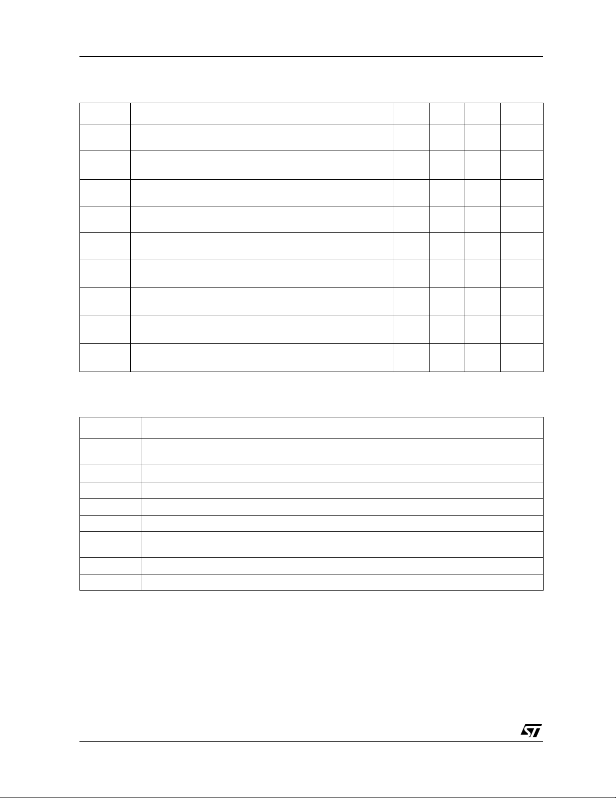
TYPICAL APPLICATION SCHEMATIC
1/19
TS4900
ABSOLUTE MAXIMUM RATINGS
Symbol Parameter Value Unit
V
T
T
R
Supply voltage
CC
V
Input Voltage
i
Operating Free Air Temperature Range -40 to + 85 °C
oper
Storage Temperature -65 to +150 °C
stg
T
Maximum Junction Temperature 150 °C
j
Thermal Resistance Junction to Ambient
thja
SO8
MiniSO8
Pd Power Dissipation
ESD Human Body Model 2 kV
ESD Machine Model 200 V
Latch-up Latch-up Immunity Class A
Lead Temperature (soldering, 10sec ) 250 °C
1. All voltages values are measured with respect to the ground pin.
2. The magnitude of input signal must never exceed V
3. Device is protected in case of over temperature by a thermal shutdown active @ 150°C.
4. Exceeding the power derating curves during a long period, will cause abnormal operation.
OPERATING CONDITIONS
1)
2)
3)
6V
GND to V
CC
175
215
4)
+ 0.3V / GND - 0.3V
CC
Internally Limited
V
°C/W
Symbol Parameter Value Unit
V
V
Supply Voltage 2.5 to 5.5 V
CC
to VCC - 1.5V
Common Mode Input Voltage Range
ICM
G
ND
Standby Voltage Input :
≤ V
V
STB
Device ON
Device OFF
R
Load Resistor 4 - 32
L
R
Thermal Resistance Junction to Ambient
thja
1)
SO8
MiniSO8
1. This thermal resistance can be reduced with a suitable PCB layout (see Power Derating Curves)
G
V
- 0.5V ≤ V
CC
ND
STB
150
190
≤ 0.5V
≤ V
STB
CC
V
V
Ω
°C/W
2/19
TS4900
ELECTRICAL CHARACTERISTICS
= +5V, GND = 0V , T
V
CC
Symbol Parameter Min. Typ. Max. Unit
= 25°C (unless otherwise specified)
amb
I
CC
I
STANDBY
Voo
Po
THD + N
PSRR
Φ
GM
GBP
1. Standby mode i s actived when Vstdby is tied to Vcc
2. Dynamic measurements - 20*log(r m s(Vout)/rms(Vripple)). Vripple is the surim posed sinus signal to Vc c @ f = 217Hz
= +3.3V, GND = 0V, T
V
CC
Supply Current
No input signal, no load
Standby Current
1)
No input signal, Vstdby = Vcc, RL = 8
Output Offset Voltage
No input signal, RL = 8
Output Power
THD = 1% Max, f = 1kHz, RL = 8
Total Harmonic Distortion + Noise
Po = 250mW rms, Gv = 2, 20Hz < f < 20kHz, RL = 8
Power Supply Rejection Ratio
f = 217Hz, RL = 8
Phase Margin at Unity Gain
M
R
= 8Ω, CL = 500pF
L
Gain Margin
R
= 8Ω, CL = 500pF
L
Gain Bandwidth Product
R
= 8
Ω
L
amb
Ω
Ω
Ω
Ω
2)
RFeed = 22K
Ω,
Vripple = 200mV rms
Ω,
= 25°C (unless otherwise specified)3)
68mA
10 1000 nA
520mV
0.7 W
0.15 %
75 dB
70 Degrees
20 dB
2MHz
Symbol Parameter Min. Typ. Max. Unit
I
CC
I
STANDBY
Voo
Po
THD + N
PSRR
Φ
GM
GBP
1. Standby mode i s actived when Vstdby is tied to Vcc
2. Dynamic measurements - 20*log(r m s(Vout)/rms(Vripple)). Vripple is the surim posed sinus signal to Vc c @ f = 217Hz
3. All electrical values are made by correlation between 2.6V and 5V measurement s
Supply Current
No input signal, no load
Standby Current
1)
No input signal, Vstdby = Vcc, RL = 8
Output Offset Voltage
No input signal, RL = 8
Output Power
THD = 1% Max, f = 1kHz, RL = 8
Total Harmonic Distortion + Noise
Po = 250mW rms, Gv = 2, 20Hz < f < 20kHz, RL = 8
Power Supply Rejection Ratio
f = 217Hz, RL = 8
Phase Margin at Unity Gain
M
R
= 8Ω, CL = 500pF
L
Gain Margin
R
= 8Ω, CL = 500pF
L
Gain Bandwidth Product
R
= 8
Ω
L
Ω
2)
RFeed = 22K
Ω,
Ω
Ω
Vripple = 200mV rms
Ω,
5.5 8 mA
10 1000 nA
520mV
300 mW
Ω
0.15 %
75 dB
70 Degrees
20 dB
2MHz
3/19
TS4900
ELECTRICAL CHARACTERISTICS
V
= 2.6V, GND = 0V, T
CC
Symbol Parameter Min. Typ. Max. Unit
= 25°C (unless otherwise specified)
amb
I
CC
I
STANDBY
Voo
Po
THD + N
PSRR
Φ
GM
GBP
1. Standby mode i s actived when Vstdby is tied to Vcc
2. Dynamic measurements - 20*log(r m s(Vout)/rms(Vripple)). Vripple is the surim posed sinus signal to Vc c @ f = 217Hz
Supply Current
No input signal, no load
Standby Current
1)
No input signal, Vstdby = Vcc, RL = 8
Output Offset Voltage
No input signal, RL = 8
Output Power
THD = 1% Max, f = 1kHz, RL = 8
Total Harmonic Distortion + Noise
Po = 200mW rms, Gv = 2, 20Hz < f < 20kHz, RL = 8
Power Supply Rejection Ratio
f = 217Hz, RL = 8
Phase Margin at Unity Gain
M
R
= 8Ω, CL = 500pF
L
Gain Margin
R
= 8Ω, CL = 500pF
L
Gain Bandwidth Product
R
= 8
Ω
L
Ω
2)
RFeed = 22K
Ω,
Ω
Ω
Vripple = 200mV rms
Ω,
5.5 8 mA
10 1000 nA
520mV
180 mW
Ω
0.15 %
75 dB
70 Degrees
20 dB
2MHz
Components Functional Description
Rin
Cin
Inverting input resistor which sets the closed loop gain in conjunction with Rfeed. This resistor also
forms a high pass filter with Cin (fc = 1 / (2 x Pi x Rin x Cin))
Input coupling capacitor which blocks the DC voltage at the amplifier input terminal
Rfeed Feed back resistor which sets the closed loop gain in conjunction with Rin
Cs Supply Bypass capacitor which provides power supply filtering
Cb Bypass pin capacitor which provides half supply filtering
Cfeed
Low pass filter capacitor allowing to cut the high frequency
(low pass filter cut-off frequency 1 / (2 x Pi x Rfeed x Cfeed))
Rstb Pull-up resistor which fixes the right supply level on the standby pin
Gv Closed loop gain in BTL configuration = 2 x (Rfeed / Rin)
REMARKS
1. All measurements, except PSRR measurements, are made with a supply bypass capacitor Cs = 100µF.
2. The standby response time is about 1µs.
4/19
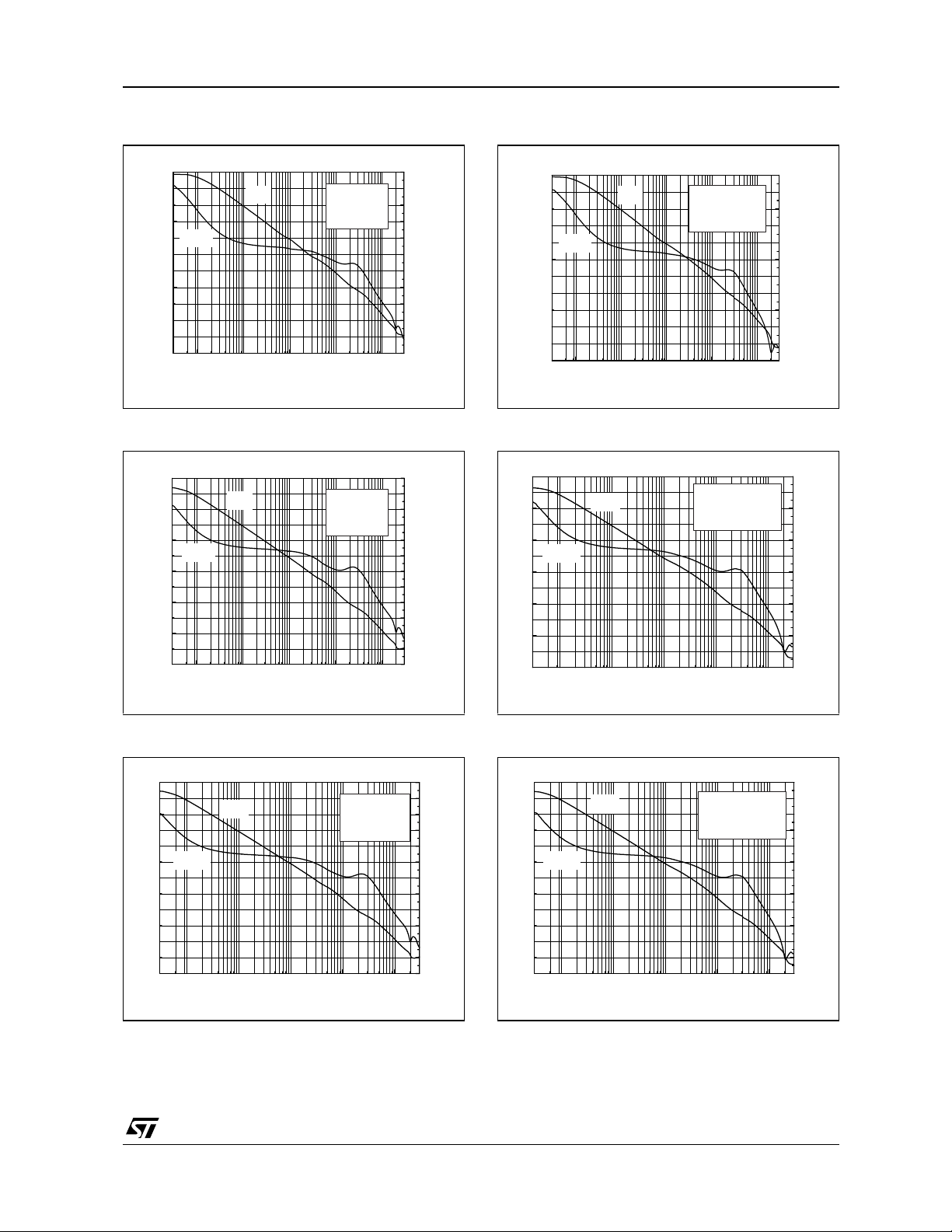
TS4900
0.3 1 10 100 1000 10000
-40
-20
0
20
40
60
80
-240
-220
-200
-180
-160
-140
-120
-100
-80
-60
-40
-20
0
Gain (dB)
Frequency (kHz)
Vcc = 3.3V
ZL = 8Ω + 560pF
Tamb = 25°C
Gain
Phase
Phase (Deg)
0.3 1 10 100 1000 10000
-40
-20
0
20
40
60
80
-240
-220
-200
-180
-160
-140
-120
-100
-80
-60
-40
-20
0
Gain (dB)
Frequency (kHz)
Vcc = 2.6V
ZL = 8Ω + 560pF
Tamb = 25°C
Gain
Phase
Phase (Deg)
Fig. 1 : Open Loop Frequency Response
0
60
40
Phase
20
Gain (dB)
0
-20
-40
0.3 1 10 100 1000 10000
Gain
Frequency (kHz)
Vcc = 5V
RL = 8
Tamb = 25°C
Ω
-20
-40
-60
-80
-100
-120
-140
-160
-180
-200
-220
Fig. 3 : Open Loop Frequency Response
80
60
40
20
Gain (dB)
0
-20
-40
0.3 1 10 100 1000 10000
Gain
Phase
Frequency (kHz)
Vcc = 33V
RL = 8
Ω
Tamb = 25°C
0
-20
-40
-60
-80
-100
-120
-140
-160
-180
-200
-220
-240
Phase (Deg)
Phase (Deg)
Fig. 2 : Open Loop Frequency Response
0
60
40
Phase
20
Gain (dB)
0
-20
-40
0.3 1 10 100 1000 10000
Gain
Frequency (kHz)
Vcc = 5V
ZL = 8Ω + 560pF
Tamb = 25°C
-20
-40
-60
-80
-100
-120
-140
-160
-180
-200
-220
Fig. 4 : Open Loop Frequency Response
Phase (Deg)
Fig. 5 : Open Loop Frequency Response
80
60
40
20
Gain (dB)
0
-20
-40
0.3 1 10 100 1000 10000
Gain
Phase
Frequency (kHz)
Vcc = 2.6V
RL = 8
Tamb = 25°C
Fig. 6 : Open Loop Frequency Response
0
-20
Ω
-40
-60
-80
-100
-120
-140
-160
-180
-200
-220
-240
Phase (Deg)
5/19
TS4900
0.3 1 10 100 1000 10000
-40
-20
0
20
40
60
80
100
-240
-220
-200
-180
-160
-140
-120
-100
-80
Gain (dB)
Frequency (kHz)
Vcc = 3.3V
CL = 560pF
Tamb = 25°C
Gain
Phase
Phase (Deg)
Fig. 7 : Open Loop Frequency Response
100
80
60
Gain
40
20
Gain (dB)
0
Vcc = 5V
CL = 560pF
-20
Tamb = 25°C
-40
0.3 1 10 100 1000 10000
Phase
Frequency (kHz)
-80
-100
-120
-140
-160
-180
-200
-220
Fig. 9 : Open Loop Frequency Response
100
80
60
Gain
40
20
Gain (dB)
0
Vcc = 2.6V
-20
CL = 560pF
Tamb = 25°C
-40
0.3 1 10 100 1000 10000
Phase
Frequency (kHz)
-80
-100
-120
-140
-160
-180
-200
-220
-240
Fig. 8 : Open Loop Frequency Response
Phase (Deg)
Phase (Deg)
6/19

TS4900
10 100 1000 10000 100000
-60
-50
-40
-30
-20
-10
Vcc = 5, 3.3 & 2.6V
Rfeed = 22kΩ, Rin = 22k
Cb = 1µF
Rg = 100Ω, RL = 8
Ω
Tamb = 25°C
Cin=22nF
Cin=100nF
Cin=220nF
Cin=330nF
Cin=1µF
PSRR (dB)
Frequency (Hz)
Fig. 10 : Power Supply Rejection Ratio (PSRR)
vs Power supply
-30
Vripple = 200mVrms
Rfeed = 22
-40
Input = floating
RL = 8
Tamb = 25°C
-50
PSRR (dB)
-60
-70
-80
10 100 1000 10000 100000
Ω
Ω
Vcc = 5V, 3.3V & 2.6V
Cb = 1µF & 0.1µF
Frequency (Hz)
Fig. 12 : Power Supply Rejection Ratio (PSRR)
vs Bypass Capacitor
-10
-20
-30
-40
-50
PSRR (dB)
-60
Cb=1µF
Cb=10µF
Vcc = 5, 3.3 & 2.6V
Rfeed = 22k
Rin = 22k, Cin = 1µF
Rg = 100Ω, RL = 8
Tamb = 25°C
Cb=47µF
Ω
Fig. 11 : Power Supply Rejection Ratio (PSRR)
vs Feedback Capacitor
-10
Vcc = 5, 3.3 & 2.6V
-20
Cb = 1µF & 0.1µF
Rfeed = 22k
-30
Vripple = 200mVrms
Input = floating
-40
RL = 8
Tamb = 25°C
-50
PSRR (dB)
-60
-70
-80
10 100 1000 10000 100000
Ω
Ω
Frequency (Hz)
Cfeed=0
Cfeed=150pF
Cfeed=330pF
Cfeed=680pF
Fig. 13 : Power Supply Rejection Ratio (PSRR)
vs Input Capacitor
-70
Cb=100µF
-80
10 100 1000 10000 100000
Frequency (Hz)
Fig. 14 : Power Supply Rejection Ratio (PSRR)
vs Feedback Resistor
-10
Vcc = 5, 3.3 & 2.6V
-20
Cb = 1µF & 0.1µF
Vripple = 200mVrms
-30
Input = floating
RL = 8
-40
-50
PSRR (dB)
-60
-70
-80
Ω
Tamb = 25°C
10 100 1000 10000 100000
Rfeed=110k
Rfeed=47k
Frequency (Hz)
Ω
Ω
Rfeed=22k
Rfeed=10k
Ω
Ω
7/19

TS4900
Fig. 15 : Pout @ THD + N = 1% vs Supply
Voltage vs RL
1.0
Gv = 2 & 10
Cb = 1µF
0.8
F = 1kHz
BW < 125kHz
Tamb = 25οC
0.6
0.4
0.2
Output power @ 1% THD + N (W)
0.0
2.5 3.0 3.5 4.0 4.5 5.0
4
Ω
Vcc (V)
8
Ω
16
Ω
32
Ω
Fig. 17 : Power Dissipation vs Pout
1.4
Vcc=5V
1.2
f=1kHz
THD+N<1%
1.0
0.8
0.6
Power Dissipation (W)
0.4
0.2
0.0
0.0 0.2 0.4 0.6 0.8 1.0
RL=16
Ω
Output Power (W)
RL=8
RL=4
Ω
Ω
Fig. 16 : Pout @ THD + N = 10% vs Supply
Voltage vs RL
1.2
Gv = 2 & 10
Cb = 1µF
1.0
F = 1kHz
BW < 125kHz
Tamb = 25°C
0.8
0.6
0.4
0.2
Output power @ 10% THD + N (W)
0.0
2.5 3.0 3.5 4.0 4.5 5.0
4
Ω
Vcc (V)
8
Ω
16
Ω
32
Ω
Fig. 18 : Power Dissipation vs Pout
0.6
Vcc=3.3V
f=1kHz
0.5
THD+N<1%
0.4
0.3
0.2
Power Dissipation (W)
0.1
0.0
0.0 0.2 0.4 0.6
RL=16
Output Power (W)
RL=8
Ω
RL=4
Ω
Ω
Fig. 19 : Power Dissipation vs Pout
0.40
Vcc=2.6V
0.35
f=1kHz
THD+N<1%
0.30
0.25
0.20
0.15
Power Dissipation (W)
8/19
0.10
0.05
0.00
0.0 0.1 0.2 0.3
RL=16
Ω
Output Power (W)
RL=8
RL=4
Ω
Fig. 20 : Power Derating Curves
Ω

TS4900
8 162432
0.0
0.2
0.4
0.6
0.8
1.0
1.2
Vcc=2.5V
Vcc=4.5V
Vcc=4V
Vcc=3.5V
Vcc=3V
Vcc=5V
THD+N=10%
Gv = 2 & 10
Cb = 1µF
F = 1kHz
BW < 125kHz
Tamb = 25°C
Output Power (W)
Load Resistance ( )
Fig. 21 : Output Power vs Load Resistance
1.0
0.8
0.6
0.4
Output power (W)
0.2
Vcc=3.5V
0.0
Vcc=5V
Vcc=4.5V
Vcc=3V
81616 24 3232
Vcc=2.5V
Load Resistance ( )
THD+N=1%
Gv = 2 & 10
Cb = 1µF
F = 1kHz
BW < 125kHz
Tamb = 25°C
Vcc=4V
Fig. 23 : Clipping Voltage vs Supply Voltage
1.0
Tamb = 25°C
0.9
0.8
0.7
0.6
0.5
Dropout Voltage (V)
0.4
0.3
0.2
2.5 3.0 3.5 4.0 4.5 5.0
4Ω Low Side
8Ω Low Side
Supply Voltage (V)
4Ω High Side
8Ω High Side
Fig. 22 : Output Power vs Load Resistance
Fig. 24 : Frequency response vs Cin & Cfeed
10
5
0
-5
-10
Gain (dB)
-15
-20
-25
10 100 1000 10000
Cin = 22nF
Cin = 82nF
Cfeed = 330pF
Cin = 470nF
Frequency (Hz)
Cfeed = 680pF
Cfeed = 2.2nF
Rin = Rfeed = 22kΩ
Tamb = 25°C
Fig. 25 : Noise Floor
100
Vcc = 2.5V to 5V
Rin = Rfeed = 22k
80
Cb = Cin = 1µF
Input Grounded
BW < 22kHz
60
Tamb = 25°C
40
Output Noise Voltage ( V)
20
0
20
Ω
V
+ V
OUT1
OUT2
100 1000 10000
Frequency (Hz)
Standby = ON
9/19

TS4900
1E-3 0.01 0.1 1
0.1
1
10
RL = 4Ω, Vcc = 5V
Gv = 10
Cb = Cin = 1µF
BW < 125kHz, Tamb = 25°C
20kHz
20Hz
1kHz
THD + N (%)
Output Power (W)
1E-3 0.01 0.1 1
0.1
1
10
RL = 4Ω, Vcc = 3.3V
Gv = 10
Cb = Cin = 1µF
BW < 125kHz
Tamb = 25°C
20kHz
20Hz
1kHz
THD + N (%)
Output Power (W)
1E-3 0.01 0.1
0.1
1
10
RL = 4Ω, Vcc = 2.6V
Gv = 10
Cb = Cin = 1µF
BW < 125kHz
Tamb = 25°C
20kHz
20Hz
1kHz
THD + N (%)
Output Power (W)
Fig. 26 : THD + N vs Output Power
10
Rl = 4
Ω
Vcc = 5V
Gv = 2
Cb = Cin = 1µF
BW < 125kHz
Tamb = 25°C
1
THD + N (%)
0.1
1E-3 0.01 0.1 1
20kHz
20Hz, 1kHz
Output Power (W)
Fig. 28 : THD + N vs Output Power
10
RL = 4Ω, Vcc = 3.3V
Gv = 2
Cb = Cin = 1µF
BW < 125kHz
Tamb = 25°C
1
THD + N (%)
20kHz
Fig. 27 : THD + N vs Output Power
Fig. 29 : THD + N vs Output Power
0.1
1E-3 0.01 0.1 1
Output Power (W)
Fig. 30 : THD + N vs Output Power
10
RL = 4Ω, Vcc = 2.6V
Gv = 2
Cb = Cin = 1µF
BW < 125kHz
Tamb = 25°C
1
THD + N (%)
20Hz, 1kHz
0.1
1E-3 0.01 0.1
10/19
Output Power (W)
20Hz, 1kHz
Fig. 31 : THD + N vs Output Power
20kHz

TS4900
1E-3 0.01 0.1 1
0.1
1
10
RL = 8
Ω
Vcc = 5V
Gv = 10
Cb = Cin = 1µF
BW < 125kHz
Tamb = 25°C
20kHz20Hz
1kHz
THD + N (%)
Output Power (W)
1E-3 0.01 0.1 1
0.1
1
10
RL = 8Ω, Vcc = 3.3V
Gv = 10
Cb = Cin = 1µF
BW < 125kHz
Tamb = 25°C
20kHz
20Hz
1kHz
THD + N (%)
Output Power (W)
1E-3 0.01 0.1
0.1
1
10
RL = 8Ω, Vcc = 2.6V
Gv = 10
Cb = Cin = 1µF
BW < 125kHz
Tamb = 25°C
20kHz
20Hz
1kHz
THD + N (%)
Output Power (W)
Fig. 32 : THD + N vs Output Power
10
RL = 8
Ω
Vcc = 5V
Gv = 2
Cb = Cin = 1µF
BW < 125kHz
Tamb = 25°C
1
THD + N (%)
0.1
1E-3 0.01 0.1 1
20Hz, 1kHz
20kHz
Output Power (W)
Fig. 34 : THD + N vs Output Power
10
RL = 8Ω, Vcc = 3.3V
Gv = 2
Cb = Cin = 1µF
BW < 125kHz
Tamb = 25°C
1
Fig. 33 : THD + N vs Output Power
Fig. 35 : THD + N vs Output Power
THD + N (%)
20Hz, 1kHz
0.1
1E-3 0.01 0.1 1
Output Power (W)
Fig. 36 : THD + N vs Output Power
10
RL = 8Ω, Vcc = 2.6V
Gv = 2
Cb = Cin = 1µF
BW < 125kHz
Tamb = 25°C
1
THD + N (%)
20Hz, 1kHz
0.1
1E-3 0.01 0.1
Output Power (W)
20kHz
Fig. 37 : THD + N vs Output Power
20kHz
11/19

TS4900
Fig. 38 : THD + N vs Output Power
10
RL = 16Ω, Vcc = 5V
Gv = 2
Cb = Cin = 1µF
BW < 125kHz
1
Tamb = 25°C
20kHz
THD + N (%)
0.1
20Hz, 1kHz
0.01
1E-3 0.01 0.1 1
Output Power (W)
Fig. 40 : THD + N vs Output Power
10
RL = 16Ω, Vcc = 3.3V
Gv = 2
Cb = Cin = 1µF
BW < 125kHz
1
Tamb = 25°C
THD + N (%)
0.1
20kHz
Fig. 39 : THD + N vs Output Power
10
RL = 16Ω, Vcc = 5V
Gv = 10
Cb = Cin = 1
BW < 125kHz
1
Tamb = 25
THD + N (%)
0.1
0.01
1E-3 0.01 0.1 1
µ
F
°
C
1kHz
Output Power (W)
20kHz
20Hz
Fig. 41 : THD + N vs Output Power
10
RL = 16
Ω
Vcc = 3.3V
Gv = 10
Cb = Cin = 1µF
1
BW < 125kHz
Tamb = 25°C
20kHz
THD + N (%)
0.1
0.01
1E-3 0.01 0.1
20Hz, 1kHz
Output Power (W)
Fig. 42 : THD + N vs Output Power
10
RL = 16
Ω
Vcc = 2.6V
Gv = 2
Cb = Cin = 1µF
1
BW < 125kHz
Tamb = 25°C
THD + N (%)
0.1
0.01
1E-3 0.01 0.1
20kHz
20Hz, 1kHz
Output Power (W)
1kHz
0.01
1E-3 0.01 0.1
20Hz
Output Power (W)
Fig. 43 : THD + N vs Output Power
10
RL = 16
Ω
Vcc = 2.6V
Gv = 10
Cb = Cin = 1µF
1
BW < 125kHz
Tamb = 25°C
THD + N (%)
0.1
1kHz
0.01
1E-3 0.01 0.1
Output Power (W)
20Hz
20kHz
12/19

TS4900
2.5 3.0 3.5 4.0 4.5 5.0
50
60
70
80
90
RL=16
Ω
RL=4
Ω
RL=8
Ω
Gv = 10
Cb = Cin = 1µF
THD+N < 0.7%
Tamb = 25°C
SNR (dB)
Vcc (V)
2.5 3.0 3.5 4.0 4.5 5.0
50
60
70
80
90
RL=16
Ω
RL=4
Ω
RL=8
Ω
Gv = 10
Cb = Cin = 1µF
THD+N < 0.7%
Tamb = 25°C
SNR (dB)
Vcc (V)
0.0 0.5 1.0 1.5 2.0 2.5 3.0 3.5 4.0 4.5 5.0
0
1
2
3
4
5
6
7
Vcc = 5V
Tamb = 25°C
Icc (mA)
Vstandby (V)
Fig. 44 : Signal to Noise Ratio vs Power Supply
with Unweighted Filter (20Hz to 20kHz)
100
90
RL=4
RL=8
RL=16
80
70
SNR (dB)
60
50
2.5 3.0 3.5 4.0 4.5 5.0
Ω
Ω
Vcc (V)
Ω
Gv = 2
Cb = Cin = 1µF
THD+N < 0.4%
Tamb = 25°C
Fig. 46 : Signal to Noise Ratio vs Power Supply
with Weig h t e d Filt e r t y p e A
110
100
RL=4
RL=8
RL=16
90
Ω
Ω
Ω
Fig. 45 : Signa l to Nois e Ratio Vs Power Supply
with Unweighted Filter (20Hz to 20kHz)
Fig. 47 : Signal to Noise Ratio vs Power Supply
with Weighted Filter Type A
80
SNR (dB)
70
60
2.5 3.0 3.5 4.0 4.5 5.0
Fig. 48 : Current C onsumpt i on vs Powe r
Supply Voltage
7
Vstandby = 0V
Tamb = 25°C
6
5
4
3
Icc (mA)
2
1
0
012345
Gv = 2
Cb = Cin = 1µF
THD+N < 0.4%
Tamb = 25°C
Vcc (V)
Fig. 49 : C urrent Consumpt ion vs Standby
Voltage @ Vcc = 5V
Vcc (V)
13/19

TS4900
0.0 0.5 1.0 1.5 2.0 2.5
0
1
2
3
4
5
6
Vcc = 2.6V
Tamb = 25°C
Icc (mA)
Vstandby (V)
Fig. 50 : C urrent Consumpt ion vs Standby
Voltage @ Vcc = 3.3V
6
5
4
3
Icc (mA)
2
1
0
0.0 0.5 1.0 1.5 2.0 2.5 3.0
Vstandby (V)
Vcc = 3.3V
Tamb = 25°C
Fig. 51 : C urrent Consumpt ion vs Standby
Voltage @ Vcc = 2.6V
14/19

TS4900
)W(
R
)Vout2(
Pout
L
2
RMS
=
■BTL Configuration Principle
The TS4900 is a monolithic power amplifier with a
BTL (Bridge Tied Load) output configuration. BTL
means that each end of the load is connected t o
two single ended output amplifiers. Thus, we have:
Single ended output 1 = Vout1 = Vout (V)
Single ended output 2 = Vout2 = -Vout (V)
And Vout1 - Vout2 = 2Vout (V)
The output power is :
For the same power supply voltage, the output
power in BTL configuration is four times higher
than the output power in single ended
configuration.
■Gain In Typical Application Schematic
(cf. page 1)
In flat region (no effect of Cin), the output voltage
of the first stage is :
Vout1 = Vin –
For the second stage : Vout2 = -Vout1 (V)
The differential output voltage is
Vout2
V o ut 1 = 2Vin –
Rfeed
------------------- - (V)
Rin
Rfeed
------------------- - (V)
Rin
bandwidth by adding a capacitor (Cfeed) in
parallel with Rfeed. Its form a low pass filter with a
-3dB cut off frequency
F
CH =
---------------------------------------------- - Hz()
2π Rf eed Cfeed
1
■Power dissipation and efficiency
Hypothesis :
• Voltage and current in the load are sinusoidal
(Vout and Iout)
• Supply voltage is a pure DC source (Vcc)
Regarding the load we have:
V
OUT = V
and
I
OUT =
and
P
OUT =
Then, the average current delivered by the supply
voltage is:
CC
AVG
= 2
I
The power delivered by the supply voltage is
Psupply = Vcc Icc
AVG
(W)
sinωt (V)
PEAK
V
OUT
---------------- - (A)
R
L
2
PEAK
V
---------------------- (W)
L
2R
PEAK
V
-------------------- (A)
L
πR
The differential gain named gain (Gv) for more
convenient usage is :
Vout2 Vout1–
Gv =
--------------------------------------- = 2
Vin
Rfeed
------------------- Rin
Remark : Vout2 is in phase with Vin and Vout1 is
180 phased with Vin. It means that the positive
terminal of the loudspeaker should be connected
to Vout2 and the negative to Vout1.
■Low and high frequency response
In low frequency region, the effect of Cin starts.
Cin with Rin forms a high pass filter with a -3dB cut
off frequency
CL =
F
In high frequency region, you can limit the
1
------------------------------- - Hz()
2π Rin Cin
Then, the po wer dissip ated by the amplifier is
Pdiss = Psupply - Pout (W)
P
22Vcc
diss =
---------------------- P OUT POUT (W)–
πR
L
and the maximum value is obtained when:
∂Pdiss
--------------------- - = 0
OUT
∂P
and its value is:
2
Vcc2
=
maxPdiss
2
π
R
)W(
L
Remark : This maximum valu e is only depending
on power supply voltage and load values.
The efficiency is the ratio between the output
15/19

TS4900
power and the power supply
η =
P
OUT
----------------------- - =
Psupply
πV
PEAK
----------------------4VCC
The maximum theoret ical value is reached when
Vpeak = Vcc, so
π
----- = 78.5%
4
■Decoupl i ng of the ci rc u it
Two capacitors are needed to bypass properly the
TS4900, a power supply bypass capacitor Cs and
a bias voltage bypass capacitor Cb.
Cs has especially an influence on the THD+N in
high frequency (above 7kHz) and indirectly on the
power supply disturbances.
With 100µF, you can expect similar THD+N
performances like shown in the datasheet.
If Cs is lower than 100µF, in high frequency
increases, THD+N and disturbances on the power
supply rail are less filtered .
To the contrary, if Cs is higher than 100µF, those
disturbances on the power supply rail are more
filtered.
Cb has an influence on THD+N in lower frequency,
but its function is critical on the final result of PSRR
with input grounded in lower frequency.
If Cb is lower than 1µF, THD+N increase in lower
frequency (see THD+N vs frequency curves) and
the PSRR worsens up
If Cb is higher than 1µF, the benefit on THD+N in
lower frequency is small but the ben efit on PSRR
is substantial (see PSRR vs. Cb curve : fig.12).
Moreover, Cb determines the speed that the
amplifier turns ON. The slower th e speed is, the
softer the turn ON noise is.
The charge time of Cb is directly proportional to
the internal generator resistance 50kΩ.
Then, the charge time constant for Cb is
τb = 50kΩxCb (s)
As Cb is directly connected to the non-inverting
input (pin 2 & 3) and if we want to minimize, in
amplitude and duration, the output spike on Vout1
(pin 5), Cin must be charged faster than Cb. T he
charge time constant of Cin is
τin = (Rin+Rfeed)xCin (s)
Thus we have the relation
τin << τb (s)
The respect of this relation permits to minimize the
pop and click noise.
Remark
: Minimize Cin and Cb has a benefit on
pop and click phenomena but also on cost and
size of the application.
Example
: your target for the -3dB cut off
frequency is 100 Hz. With Rin=Rfeed=22 kΩ,
Cin=72nF (in fact 82nF or 100nF).
With Cb=1µF, if you choose the one of the latest
two values of Cin, the pop and click phenomena at
power supply ON or standby function ON/OFF will
be very small
50 kΩx1µF >> 44kΩx100nF (50ms >> 4.4ms).
Increasing Cin value increas es the pop and click
phenomena to an unpleasant sound at power
supply ON and standby function ON/OFF .
Why Cs is not important in pop and click
consideration ?
Note that Cin has a non-negligible effect on PSRR
in lower frequency. Lower is its value, higher is the
PSRR (see fig. 13 ).
■Pop and Click performanc e
Pop and Click performance is intimately linked
with the size of the input capacitor Cin and the bias
voltage bypass capacitor Cb.
Size of Cin is du e to the lower cut-off frequency
and PSRR value requested. Size of Cb is due to
THD+N and PSRR requested always in lower
frequency.
16/19
Hypothesis :
• Cs = 100µF
• Supply voltage = 5V
• Supply voltage internal resistor = 0.1Ω
• Supply current of the amplifier Icc = 6mA
At power ON of the supply, the supply capacitor is
charged through the internal power supply
resistor. So, to reach 5V you need about five to ten
times the charging time constant of Cs (τs =
0.1xCs (s)).
Then, this time equal 50µs to 100µs << τb in the
majority of application.

TS4900
At power OFF of the supply, Cs is discharged by a
constant current Icc. The di scharge time from 5V
to 0V of Cs is
tDischCs =
5Cs
------------- - = 83 ms
Icc
Now, we must consider the discharge time of Cb.
At power OFF or standby ON, Cb is discharged by
a 100kΩ resistor. So the discharge time i s about
τb
≈ 3xCbx100kΩ (s).
Disch
In the majority of application, Cb=1µF, then
τb
≈300ms >> t
Disch
dischCs
.
■ How to use the PSRR curves (page 7)
We have finished a design and we have ch osen
the components values :
• Rin=Rfeed=22kΩ, Cin=100nF, Cb=1µF
Now, on fig. 13, we can see the PSRR (input
grounded) vs frequency curves. At 217Hz we have
a PSRR value of -36dB.
In fact, we want a value of abou t -70dB. So, we
need a gain of +34dB !
Now, on fig. 12 we can see the effect of Cb on the
PSRR (input grounded) vs. frequency. With
Cb=100µF, we can reach the -70dB value.
The process to obtain the final curve (Cb=100µF,
Cin=100nF, Rin=Rfeed=22kΩ) is a simple transfer
point by point on each frequency of the curve on
fig. 13 to the curve on fig. 12.
The measurement result is shown on figure A.
Fig. A : PSRR changes with Cb
■Rem ark on PSRR m easu remen t cond itions
What is the PSRR ?
The PSRR is the Power Suppl y Rejection Ratio.
It's a kind of SVR in a determined frequency range.
The PSRR of a device is the ratio between the
power supply disturbance and the result on the
output. We can say that the P SRR is t he a bility of
a device to m inimize the impact o f power supply
disturbances to the output.
How do we measure the PSRR ?
Fig. B : PSRR measurement schematic
Rfeed
-
+
Bias
6
Vcc
GND
Av=-1
+
Vout1
Vout2
5
8
TS4900
Vs-
RL
Vs+
Vripple
Vcc
Rin
Cin
Rg
100 Ohms
Cb
4
3
2
1
Vin-
Vin+
Bypass
Standby
■Measurement process:
• Fix the DC voltage supply (Vcc)
• Fix the AC sinusoidal ripple voltage (Vripple)
• No bypass capacitor Cs is used
-30
Cin=100nF
-40
Cb=1µF
-50
PSRR (dB)
-60
-70
10 100 1000 10000 100000
Cin=100nF
Cb=100µF
Vcc = 5, 3.3 & 2.6V
Rfeed = 22k, Rin = 22k
Rg = 100Ω, RL = 8
Tamb = 25°C
Frequency (Hz)
Ω
The PSRR value for each frequency is :
PSRR dB() = 20 x Log10
Remark :
The measurement of the RMS voltage is
Rms V
---------------------------------------- ----Rms Vs
ripple()
- Vs
()
+
-
not a selective RMS measurement but a full range
(2 Hz to 125 kHz) RMS measurement. This means
we have: the effective RMS signal + the noise.
17/19

TS4900
PACKAGE MECHANICAL DATA
8 PINS - PLASTIC MICROPACKAGE (SO)
A
a2
L
c1
C
a3
b
e3
D
8
M
5
s
a1
E
b1
F
1
4
Millimeters Inches
Dim.
Min. Typ. Max. Min. Typ. Max.
A 1.75 0.069
a1 0.1 0.25 0.004 0.010
a2 1.65 0.065
a3 0.65 0.85 0.026 0.033
b 0.35 0.48 0.014 0.019
b1 0.19 0.25 0.007 0.010
C 0.25 0.5 0.010 0.020
c1 45° (typ.)
D 4.8 5.0 0.189 0.197
E 5.8 6.2 0.228 0.244
e 1.27 0.050
e3 3.81 0.150
F 3.8 4.0 0.150 0.157
L 0.4 1.27 0.016 0.050
M 0.6 0.024
S 8° (max.)
18/19

PACKAGE MECHANICAL DATA
8 PINS - PLASTIC MICROPACKAGE (miniSO)
0,25mm
c
E1
.010inch
GAGEPLANE
PLANE
SEATING
TS4900
k
L
L1
C
A2
A1
D
b
C
5
8
EA
4
e
1
ccc
PIN1IDENTIFICA TION
Dim. Millimeters Inches
Min. Typ. Max. Min. Typ. Max.
A 1.100 0.043
A1 0.050 0.100 0.150 0.002 0.004 0.006
A2 0.780 0.860 0.940 0.031 0.034 0.037
b 0.250 0.330 0.400 0.010 0.013 0.016
c 0.130 0.180 0.230 0.005 0.007 0.009
D 2.900 3.000 3.100 0.114 0.118 0.122
E 4.750 4.900 5.050 0.187 0.193 0.199
E1 2.900 3.000 3.100 0.114 0.118 0.122
e 0.650 0.026
L 0.400 0.550 0.700 0.016 0.022 0.028
L1 0.950 0.037
k 0d3d6d0d3d6d
ccc 0.100 0.004
Information furnished is bel ieved to be accurate and reliable. However, STMicroe lectronics assumes no responsibility for the
consequences of use of such information nor for any infringement of patents or other rights of third parties which may result from
its use. No li cense is granted by i mp lication or otherwise under any patent or patent rights of STMicroelec tron ic s. S pec ificat ions
mentioned in this publication ar e subject to change without notice. This publication supersedes and replaces all information
previously supplied. S TMicroelectronics products are not authorized for use as critica l components in life suppo rt devices or
systems without express written approval of STMicroelectronics.
© The ST logo is a registered trademark of STMicroelectronics
© 2002 STM icroelectronics - P r i n ted in Italy - All Rights Reserved
STMicr o el ectronics GROUP OF COMPA NI ES
Australi a - Brazil - Canada - Chin a - F i nl and - France - Germany - Hong Kong - India - Israel - Italy - Japa n - Malaysia
Malta - Mor occo - Singapore - Spain - Sweden - S wi t zerland - U ni ted Kingdom - United Sta tes
© http://www.st.com
19/19
 Loading...