

TDA4443
MULTISTANDARDVIDEO IF AMPLIFIER
.
SWITCHING OFF THE IF AMPLIFIER WHEN
OPERATINGIN VTR MODE
.
DEMODULATION OF NEGATIVE OR POSITIVE IF SIGNALS. THE OUTPUT REMAINS
ON THE SAMEPOLARITYIN EVERYCASE
.
IF AGC AUTOMATICALLY ADJUSTED TO
THEACTUALSTANDARD
.
TWOAGCPOSSIBILITIESFOR B/G MODE :
1. GATEDAGC
2. UNGATED AGC ON SYNC. LEVEL AND
CONTROLLED DISCHARGE DEPENDENT
ON THE AVERAGESIGNAL LEVELFORVTR
ANDPERITV APPLICATIONS
FOR STANDARD L : FAST AGC ON PEAK
WHITEBY CONTROLLEDDISCHARGE
.
POSITIVEOR NEGATIVEGATINGPULSE
.
EXTREMELYHIGH INPUTSENSITIVITY
.
LOW DIFFERENTIALDISTORTION
.
CONSTANTINPUT IMPEDANCE
.
VERYHIGHSUPPLYVOLTAGEREJECTION
.
FEWEXTERNALCOMPONENTS
.
LOW IMPEDANCE VIDEO OUTPUT
.
SMALLTOLERANCESOF THE FIXED VIDEO
SIGNALAMPLITUDE
.
ADJUSTABLE, DELAYED AGC FOR PNP
TUNERS
DESCRIPTION
TheTDA4443 is a Video IF amplifier with standard
switchfor multistandardcolourormonochromeTV
sets,and VTR’s.
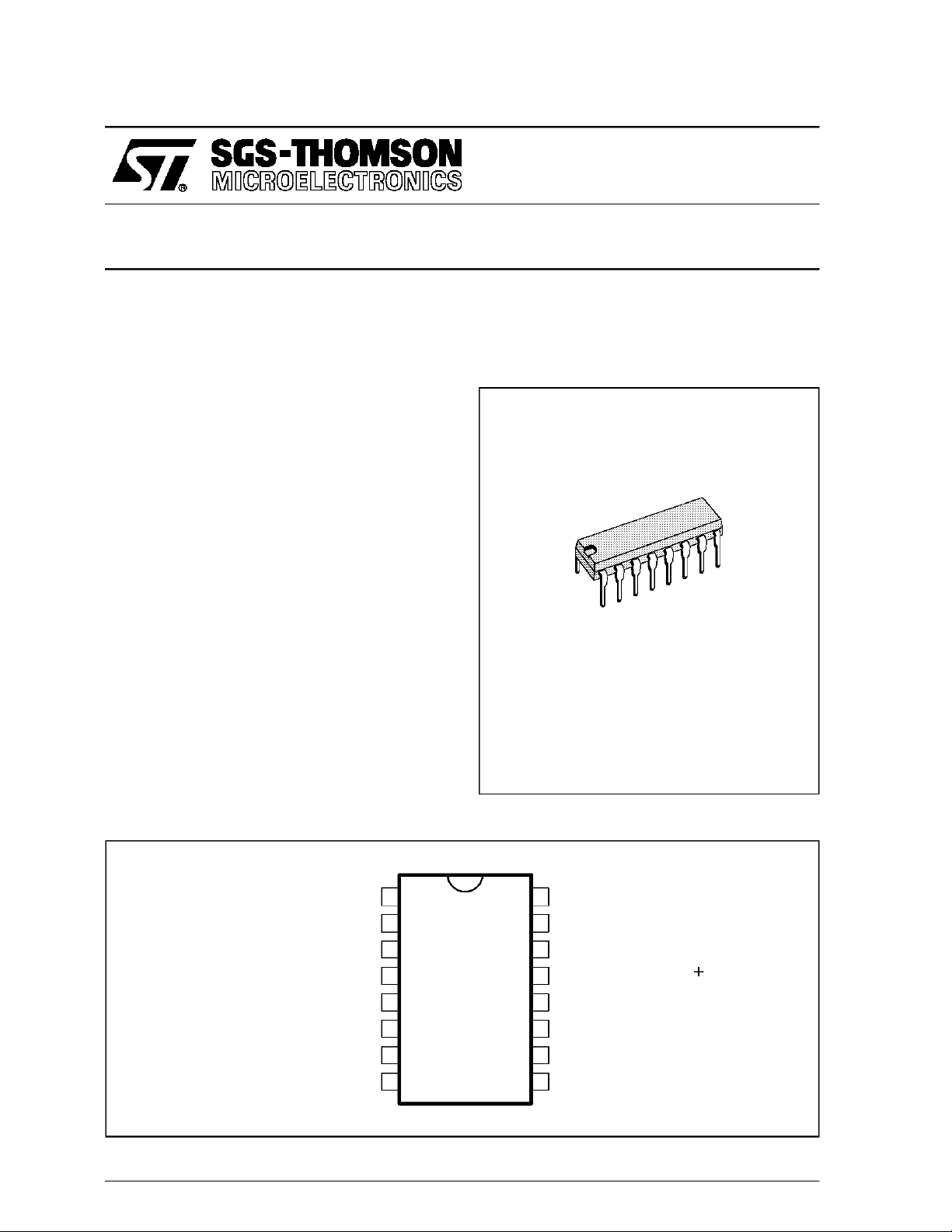
DIP16
(Plastic Package)
ORDER CODE : TDA4443
PINCONNECTIONS
STANDARD SWITCHING
IF AGC TIMECONSTANT
DELAYED TUNER AGC OUTPUT
REFERENCE LC NETWORK
December 1992
IF INPUT
GROUND
TUNERAGC ADJUST
GATINGPULSE INPUT
1
2
3
4
5
6
7
8
16
15
14
13
12
11
10
IF INPUT
GROUND
NOT TO BE CONNECTED
SUPPLYVOLTAGE V
NOT TO BE CONNECTED
VIDEO SIGNAL OUTPUT
DISCHARGETIME CONSTANT
9
REFERENCELC NETWORK
CC
4443-01.EPS
1/7
TDA4443
BLOCK DIAGRAM
VIDEO
OUTPUT
IF INPUT
IF INPUT
V
S
TDA4443
16
1
3
15
STANDARD
WIDEBANDAMPLIFIER DEMODULATOR
CONTROL
AMPLIFIER
TUNER
CONTROL
SWITCH
2
TUNER
AGC
OUTPUT
TUNER
AGC
ADJUST
SUPPLY
UNIT
1345 6
V
CC
11 10
IW
VIDEO
GATING
AMPLIFIER
9
8
GATING
7
PULSE
4443-02.EPS
GENERALDESCRIPTION
This video IF processing circuit integratesthe followingfunctionalblocks :
.
Three symmetrical, very stable, gain controlled
wideband amplifier stages - without feedback
by a quasi-galvaniccoupling.
.
Demodulatorcontrolled by the picture carrier
.
Video output amplifier with high supplyvoltage
rejection
.
Polarityswitch for the video outputsignal
.
AGC onpeakwhite level
.
GatedAGC
.
Dischargecontrol
.
Delayedtuner AGC
.
At VTR Reading mode the video output signal
isat ultrawhite level
2/7
ABSOLUTEMAXIMUM RATINGS
Symbol Parameter Value Unit
V
CC
V
0
V
ext
I
4
I
2
I
0
I
0
P
tot
T
j
T
AMB
T
stg
Supply Voltage RangePin 13 15 V
Open Loop Voltage Pin 5 max. V
CC
External Voltage Pin 4 12 V
Control Current for VTR Mode Pin 4 0.3 mA
Control Current for Standard Mode Pin 2 0.5 mA
Max. Video Output Current Pin 11 5 mA
Short Circuit Current (t ≤ 1sec) Pin 11
30 mA
Power Dissipation 1 W
Junction Temperature 125
Ambient Temperature Range 0 to +70
Storage Temperature Range -25 to +125
THERMALDATA
TDA4443
V
o
C
o
C
o
C
4443-01.TBL
Symbol Parameter Value Unit
R
th (j-a)
Junction-ambient Thermal Resistance 70
ELECTRICAL OPERATING CHARACTERISTICS
=25oC, VCC=12V,unless otherwise spacified.Test Circuit Page5.
T
AMB
Symbol Parameter Pin Min. Typ. Max. Unit
V
CC
I
CC
V
11
V
AA
V
O
V
O
∆(Vp−V
V
− V
p
blank
∆Vblack
∆Vwhite
∆Vvideo
Bvideo Video Bandwidth at -3dB 11 6 MHz
∆Vvideo
I
O
I
7
V
7
V
1
I Control Current for Status B (see status of mode switching)
Supply Voltage 13 10 12 15 V
Supply Current (VCC= 12V, V4= 3.5V,VIN=0)
13 55 75 mA
Pin 6, PIn7, PIn 2 open
Ultra White Level at Standard B/G
= 15V, V4= 3.5V
V
CC
Ultra Black Clamping Level at Standard B/G
11 4.8 5.1 5.6 V
11 1.70 1.85 2.10 V
SIGNAL 1
Picture to sync. output voltage of the video signal without load in
11 2.6 2.9 3.3 V
standard B/G (residual carrier 10%) SIGNAL 1
Picture to blanking level output voltage of thevideo signal without
11 1.80 2.1 2.40 V
load in standard L (blanking level at 28%of carrier amplitude)
SIGNAL 2 (residual carrier 5%)
)
blank
Output voltagechange of the picture to blanking level from
standard L tostandard B/G (mode BG : signal 1, mode L : signal 2)
11 10 %
Supply voltage influence on the ultra black level in standard B/G 11 0.5 %V
Supply voltage influence on the ultra white level in standard B/G 11 1 %V
Video Bandwidth
Video Signal Attenuation with V
at 4.43MHz
IN
11 1 1.5 dB
Video frequency response changes witin the AGC range 11 0.5 2.0 dB
DC Output Current(V11= 10V, VCC= 15V) 11 1.5 2 mA
Gating Pulse Current 7 0.30 1.0 mA
DC Voltage at Gating Input 7 1.3 1.6 V
Input Voltage Sensitivity VIN(with V
Standard B/G SIGNAL 1
OUT=VO
- 3dB)
1-
16
120
21040µ
=5V
V
2
o
C/W
PP
PP
µV
RMS
A
4443-02.TBL
4443-03.TBL
3/7

TDA4443
ELECTRICAL OPERATING CHARACTERISTICS (continued)
=25oC, VCC=12V, unlessotherwise spacified.TestCircuitPage 5.
T
AMB
Symbol Parameter Pin Min. Typ. Max. Unit
I Control Current Status C(see status of mode switching) - V
∆G
I
AGC
∆AGC
IF AGC Range 60 dB
IF
Available Tuner AGC Current (10dB above the AGCstarting point) 5 8 12 mA
Delay Between Tuner AGC and IF AGC (pin 6 not connected) 5 50 dB
IF residual carrier at the video o/p withing the
VIF
V2IF
AGC range 38.9MHz
77.8MHz
d Differential Distortion on Composite VIdeoSignal Amplitude
SIGNAL 3
aM Attenuationof sound tocolor carrierintermodulation signal (1.07MHz)
referred to the demodulated color carrier : PIcture Carrier = 0dB,
Color Carrier = -6dB, Sound Carrier = -24dB
∆Sync
Sync. Pulse Compression within the IF AGC Range 3 %
Sync
RI
CI
InputImpedance : Resistance
Capacitance
V Switch off Control Voltage for VTR Mode 4 9 10 V
I Switch off Current for VTR Mode 4 150 µ
= 6.3V 2 60 400 µ
2
11
11
20
50
11 5 %
11 50 dB
1-16
1-16
2.5
2
mV
mV
kΩ
pF
A
RMS
RMS
A
4443-04.TBL
SIGNAL1 (standard B/G)
DemodulatedSignal
1000mV
300mV
0mV
100%
IF Signal
100% 10%
4443-03.EPS / 4443-04.EPS
4/7

SIGNAL2 (standard L)
TDA4443
DemodulatedSignal
1000mV
300mV
0mV
SIGNAL3
100%
Demodulated Signal
900mV
500mV
IF Signal
5%
100%
4443-05.EPS/ 4443-06.EPS
4.43MHz
200mV
200mV
TEST CIRCUIT
Attenuateur
Modulator
Video
Generator
MODESWITCHING
300mV
0mV
47nF 22nF
22nF
22nF
4.43MHz
SUPPLY
VOLTAGE
22µF
10nF
V
CC
N.C.N.C.
VIDEO
OUTPUT
68nF
910111213141516
TDA4443
12345678
5k
200k
20kΩ
V4I
2.5kΩ
5
Ω
2.2µF
Ω
GATING
4443-07.EPS
33pF 0.5µH
4443-08.EPS
5/7

TDA4443
DEFINITION OF MODE SWITCHING
Status Pin 2 Pin 4 Function
A Not connected NoExternal Voltage Standard B/G mode, gatedcharge and discharge.
B 12V
HIgh Impedance
C 12V
Low Impedance
D No specifications ≥
The gating pulse at Pin 7 is internallyswitched off.
STATUSOFMODE SWITCHING, REFERRINGTO CONTROL VOLTAGE PIN2
Control Voltage
Pin 2
1.2to 2.5V* Open A Standard B/G gated sync. operation
3.0 to 5.0V High Impedance B Standard B/G, no sync., operation
> 6.5V Low Impedance C Standard L
0.0 to 0.8V Ground D Standard L
* Voltagemeasured on Pin 2.
No External Voltage Standard B/G, ungated, charging up to sync. level, discharging
dependant from average signal (peri operation).
No External Voltage At standard L ungated, charging up to peak white level,
discharge dependant from average signal level, inverted polarity
of the video output.
7.5V
In VTR reading mode the IF amplifier is blocked, turned gain
controlled down : the video output signal is fixed at constant ultra
white level forstandard B/G mode.
Connections of
Pin 2
Status Function
4443-05.TBL
4443-06.TBL
DA B CSTATUS
0.8
2.5
5.0 6.5
1.2
3.0
I2 (nA)
3
2
1
0
+12V
I2
TDA4443
V2
04812
V2
V2 (V)
4443-09.EPS
6/7

PACKAGE MECHANICAL DATA
16 PINS - PLASTICDIP
TDA4443
I
L
b1
E
Dimensions
a1
Z
b
16
18
Be
e3
D
9
F
Millimeters Inches
Min. Typ. Max. Min. Typ. Max.
a1 0.51 0.020
B 0.77 1.65 0.030 0.065
b 0.5 0.020
b1 0.25 0.010
D 20 0.787
E 8.5 0.335
e 2.54 0.100
e3 17.78 0.700
F 7.1 0.280
i 5.1 0.201
L 3.3 0.130
Z 1.27 0.050
PM-DIP16.EPS
DIP16.TBL
Information furnishedis believed to beaccurate andreliable. However, SGS-THOMSON Microelectronics assumes no responsibility
for the consequences of use ofsuch information norfor anyinfringement ofpatents or other rights of third parties which may result
from itsuse. Nolicence is granted by implication orotherwise under any patent or patent rights of SGS-THOMSON Microelectronics.
Specifications mentioned in this publication are subject to change without notice. This publication supersedes and replaces all
information previously supplied. SGS-THOMSON Microelectronics productsare not authorized for use ascritical components in life
support devices or systems without express written approval of SGS-THOMSON Microelectronics.
1994 SGS-THOMSON Microelectronics - All Rights Reserved
Purchase of I
2
I
C Patent. Rights touse these components in aI2C system, isgranted provided that thesystem conforms to
Australia - Brazil - China - France - Germany - Hong Kong - Italy - Japan- Korea - Malaysia - Malta - Morocco
The Netherlands - Singapore - Spain - Sweden - Switzerland -Taiwan - Thailand - United Kingdom - U.S.A.
2
C Components of SGS-THOMSON Microelectronics, conveys a license under the Philips
2
the I
C Standard Specifications as definedby Philips.
SGS-THOMSON Microelectronics GROUP OFCOMPANIES
7/7
 Loading...