

Page 1
TELEFUNKEN Semiconductors
TDA4439
Video IF Amplifier for Multistandard TV and VTR
Technology: Bipolar
Features
D
Standard B/G-L suitable, processes negatively and
positively modulated IF-signals with equal polarity of
the output signal
D
Ultra white inverter and ultra black limiter for reducing transmission interference
D
Internally noise protected gain control, no flyback
pulses required
D
Expanded video frequency response allows the demodulation of amplitude modulated MAC signals
Case: DIP18
D
High input sensitivity
D
Fast AGC by controlled discharge of the AGC capacitor
Standard L mode: AGC acting on peak white level,
capacitor discharge control by averaged video signal
Standard B/G: AGC acting on the sync. pulse peak
D
The direction of the AFC curve is selectable independently from the standard switch
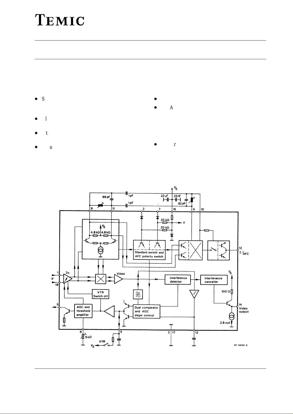
Figure 1. Block diagram
Rev . A1: 14.09.1995 1 (7)
Page 2
TDA4439
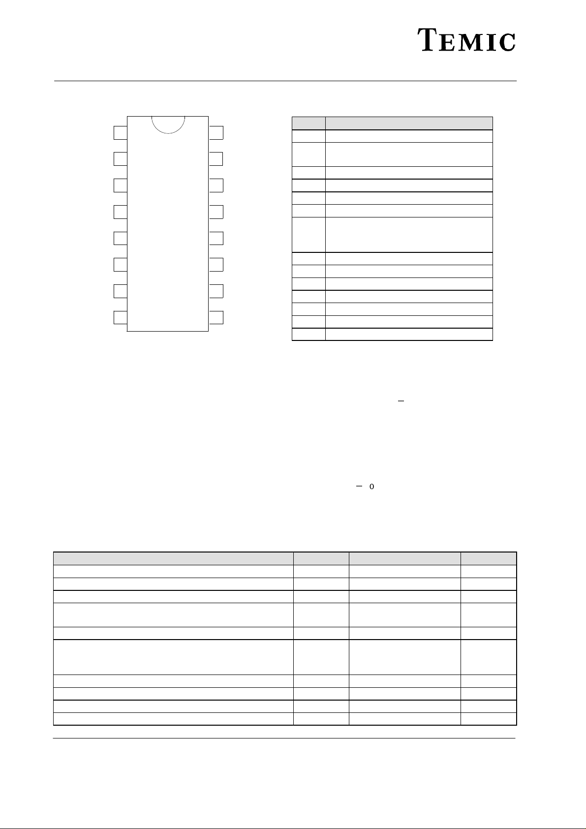
Pin Description
TELEFUNKEN Semiconductors
1
16
1, 18 IF input
2 Standard switch: open B/G
Pin Function
2
15
ground L
3, 17 Ground
3
14
4 IF-AGC storage capacitor
5 AGC (tuner control)
4
13
6 Tuner AGC take over
7 Polarity switch:
5
6
12
11
8, 11 Demodulator circuit
9, 10 AFC circuit
open AFC “DOWN”
ground AFC
“UP”
12 AFC output
7
10
13 Average capacitor standard L
14 Video output
8
95 10840
9
15 Supply voltage
16 n.c.
Circuit Description
The following function units are integrated in this circuit combination for video-IF processing:
– Three symmetric, highly stable, gain controlled wide-
band amplifier, quasi galvanic coupling eliminates
feed back
– Video carrier controlled demodulator of high linearity
– Polarity switch over for video and AFC-signal
– Video output amplifier with low-pass characteristics,
limiter for ultra black and inverter for ultra white
interference
– Disconnectable AFC * generator with push pull
current output
– High impedance, interference free controlled voltage
facilities, best possible AGC time constant with small
storage capacitor
– Controlled discharge circuit for fast gain control
– With VTR * operation the video output level is
according to the ultra white level in B/G, ultra black
level in L
Absolute Maximum Ratings
Reference point pin 3, unless otherwise specified
Parameters Symbol Value Unit
Supply voltage Pin 15 V
Supply current Pin 15 I
Open loop voltage Pin 5 V
External voltage Pin 4
Pin 14
Breaking current for VTR operation Pin 4 I
Video output current
max load Pin 14
short circuit max 1 s Pin 14
Power dissipation T
Junction temperature T
Ambient temperature range T
Storage temperature range T
≤ 60°C P
amb
V
V
I
tot
amb
stg
S
14
4
0
S
10 to 15 V
75 mA
5
4
V
10
S
8
V
V
V
0.5 mA
5
mA
50
1.0 W
j
125 °C
–25 to +70 °C
–25 to +125 °C
Rev . A1: 14.09.19952 (7)
Page 3
TELEFUNKEN Semiconductors
Thermal Resistance
Parameters Symbol Maximum Unit
Junction ambient R
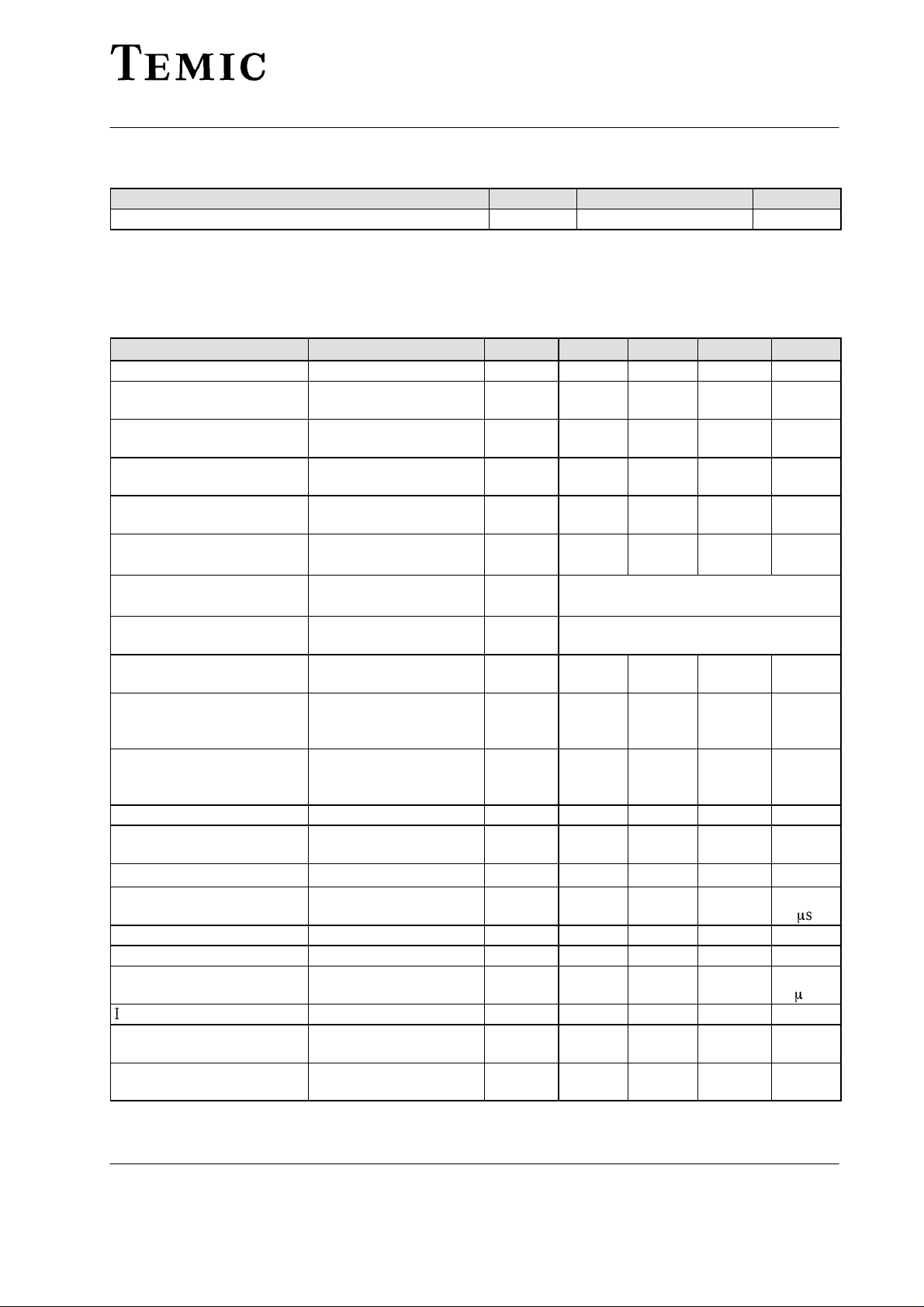
Electrical Characteristics
thJA
TDA4439
60 K/W
V
= 12 V, T
S
= 25°C, Reference point Pin 3, unless otherwise specified
amb
Parameters Test Conditions / Pins Symbol Min. Typ. Max. Unit
Supply current Pin 15 I
Ultra white level at
1)
standard B/G Pin 14 v
Ultra black clamping level
at standard B/G
Composite video output
2)
Pin 14 v
signal B/G Peak to peak Pin 14 v
Video signal standard L
3)
(black/white) Peak to peak Pin 14 v
Difference of the video
signals
standard L-B/G
Pin 14 ∆ 10 %
Clamping level of black
limiter
Pin 14 V
Threshold of the ultra white
inverter
Pin 14 V
Grey level of the ultra white
inverter
Pin 14 V
Supply voltage influence on
the ultra black level in
standard B/G
Pin 14 ∆ 0.5 %/V
Supply voltage influence on
the ultra white level in
standard B/G
Pin 14 ∆ 1.0 %/V
Video bandwidth –3 dB Pin 14 B
Video frequency response
over the AGC control range
Output DC current
Response time of the peak
V
= 8 V Pin 14
14
4)
Pin 14 ∆V
white control in standard L Pin 4 t
Voltage level standard B/G
Voltage level standard L
Input sensitivity (sym.)
5)
5)
6)
v14=3.0 Vpp,
= 0.8 V Pin 1–18 v
V
4
Pin 2 V
Pin 2 V
IF-AGC gain reduction ∆v
Available tuner AGC
10 dB via AGC use
Pin 5 I
Automatic tuner AGC with
IF-control Pin 6 n.c.
Pin 5 AGC 61 dB
S
0
0
0
0
14
14
14
video
video
I
14
r
2
2
i
p
5
65 mA
4.8 5.2 5.6 V
1.75 1.9 2.05 V
2.7 3.0 3.3 V
1.85 2.1 2.35 V
250 mV below Sync. (typ.)
900 mV upper ultra white level (typ.)
3.6 V
10 MHz
2.0 dB
2.8 mA
2 V
10
S
m
0 1.2 V
120
m
60 dB
3 4 mA
s
V
V
Rev . A1: 14.09.1995 3 (7)
Page 4
TDA4439
TELEFUNKEN Semiconductors
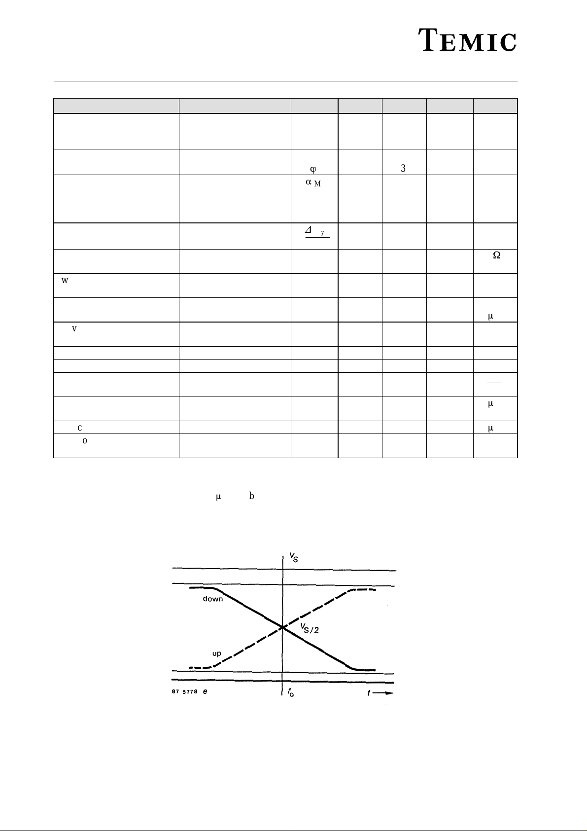
UnitMax.Typ.Min.SymbolTest Conditions / PinsParameters
IF-residual voltage at the
video output in the AGC
f = 38.9 MHz Pin 14
f = 77.8 MHz Pin 14
v 10
20
mV
area
Differential gain error Pin 14 d 3 5 %
Differential phase error Pin 14
Sound-chroma beat (1.07
MHz intermodulation) relating to demodulated auxiliary
colour carrier
Video carrier = 0 dB
Pin 14
Colour carrier = –6 dB
Sound carrier = –24 dB
Upsetting factor sync. pulse
Input impedance Pin 1–18
Pin 1–18
ö
a
IM
D
V
sync
V
sync
R
i
C
i
3 5 degree
50 dB
3 %
1.6
2
k
pF
Switch OFF voltage for
VTR-operation
Pin 4 V
4
8 10 V
Switch OFF current for
VTR-operation
Pin 4 I
4
150
m
DC voltage at the
AFC circuit
Pins 9 and 10 V 5.0 V
Scope of the AFC voltage Pin 12 V 1.0 VS–1.5 V
AFC current Pin 12 i
12
0.8 mA
AFC transconductance Pin 12 g 0.2 mA
100kHz
AFC residual current
V
= V
12
/2 Pin 12
S
±I
R
10
m
(AFC ”OFF”)
AFC current – OFF Pins 9 and 10 I
AFC polarity switching volt-
7)
age
“AFC-up” Pin 7
“AFC-down”
OFF
V
7
100 150
0
2
1.2
V
m
S
W
A
A
A
V
1)
All measurements Pin 14 without load
2)
Residual carrier 10 %3), Blanking level 30 % carrier amplitude
4)
A peak white value for at least 10 ms must be transmitted for each complete frame
5)
Direct control of standard reversing switch with TTL level
6)
Sync peak value standard B/G
7)
AFC polarity switch may be directly matched to TTL-output (i.e. processor output)
Figure 2. AFC characteristics/polarity
Rev . A1: 14.09.19954 (7)
Page 5
TELEFUNKEN Semiconductors
TDA4439
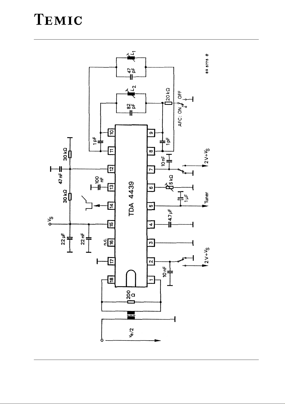
Coil data: Toko 7 KN
L
=6 turns, 0.2 CuL
1
L
=4 turns, 0.2 CuL
2
Figure 3. Test circuit
Rev . A1: 14.09.1995 5 (7)
Page 6
TDA4439
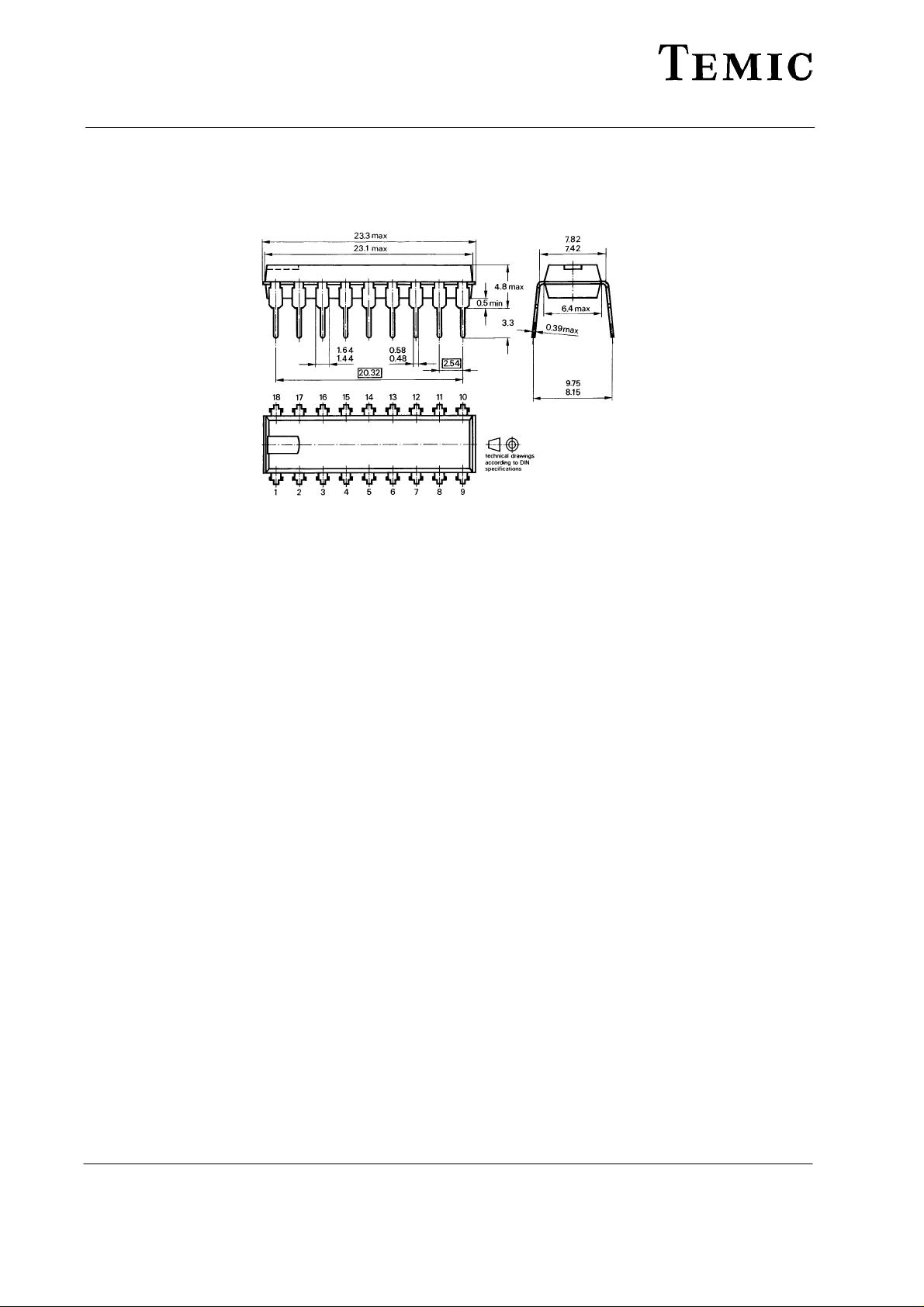
Dimensions in mm
Package: DIP 16
TELEFUNKEN Semiconductors
94 8877
Rev . A1: 14.09.19956 (7)
Page 7

TELEFUNKEN Semiconductors
TDA4439
Ozone Depleting Substances Policy Statement
It is the policy of TEMIC TELEFUNKEN microelectronic GmbH to
1. Meet all present and future national and international statutory requirements.
2. Regularly and continuously improve the performance of our products, processes, distribution and operating systems
with respect to their impact on the health and safety of our employees and the public, as well as their impact on
the environment.
It is particular concern to control or eliminate releases of those substances into the atmosphere which are known as
ozone depleting substances (ODSs).
The Montreal Protocol ( 1987) and its London Amendments (1990) intend to severely restrict the use of ODSs and
forbid their use within the next ten years. Various national and international initiatives are pressing for an earlier ban
on these substances.
TEMIC TELEFUNKEN microelectronic GmbH semiconductor division has been able to use its policy of
continuous improvements to eliminate the use of ODSs listed in the following documents.
1. Annex A, B and list of transitional substances of the Montreal Protocol and the London Amendments respectively
2. Class I and II ozone depleting substances in the Clean Air Act Amendments of 1990 by the Environmental
Protection Agency (EPA) in the USA
3. Council Decision 88/540/EEC and 91/690/EEC Annex A, B and C (transitional substances) respectively.
TEMIC can certify that our semiconductors are not manufactured with ozone depleting substances and do not contain
such substances.
We reserve the right to make changes to improve technical design and may do so without further notice.
Parameters can vary in different applications. All operating parameters must be validated for each customer
application by the customer. Should the buyer use TEMIC products for any unintended or unauthorized
application, the buyer shall indemnify TEMIC against all claims, costs, damages, and expenses, arising out of,
directly or indirectly, any claim of personal damage, injury or death associated with such unintended or
unauthorized use.
TEMIC TELEFUNKEN microelectronic GmbH, P.O.B. 3535, D-74025 Heilbronn, Germany
Telephone: 49 (0)7131 67 2831, Fax number: 49 (0)7131 67 2423
Rev . A1: 14.09.1995 7 (7)
 Loading...