


TDA2030
14W Hi-Fi AUDIO AMPLIFIER
DESCRIPTION
The TDA2030 is a monolithic integratedcircuit in
Pentawatt package, intended for use as a low
frequency class AB amplifier. Typically it provides
14W outputpower (d = 0.5%) at 14V/4Ω;at±14V
or 28V,the guaranteed output power is 12W on a
4Ω load and 8W ona 8Ω (DIN45500).
TheTDA2030provideshigh outputcurrentandhas
very lowharmonicand cross-overdistortion.
Further the device incorporates an original (and
patented) short circuit protection system comprising an arrangement for automatically limiting the
dissipated power so as to keep the working point
of the output transistorswithintheir safeoperating
ORDERING NUMBERS : TDA2030H
area.A conventionalthermal shut-down system is
also included.
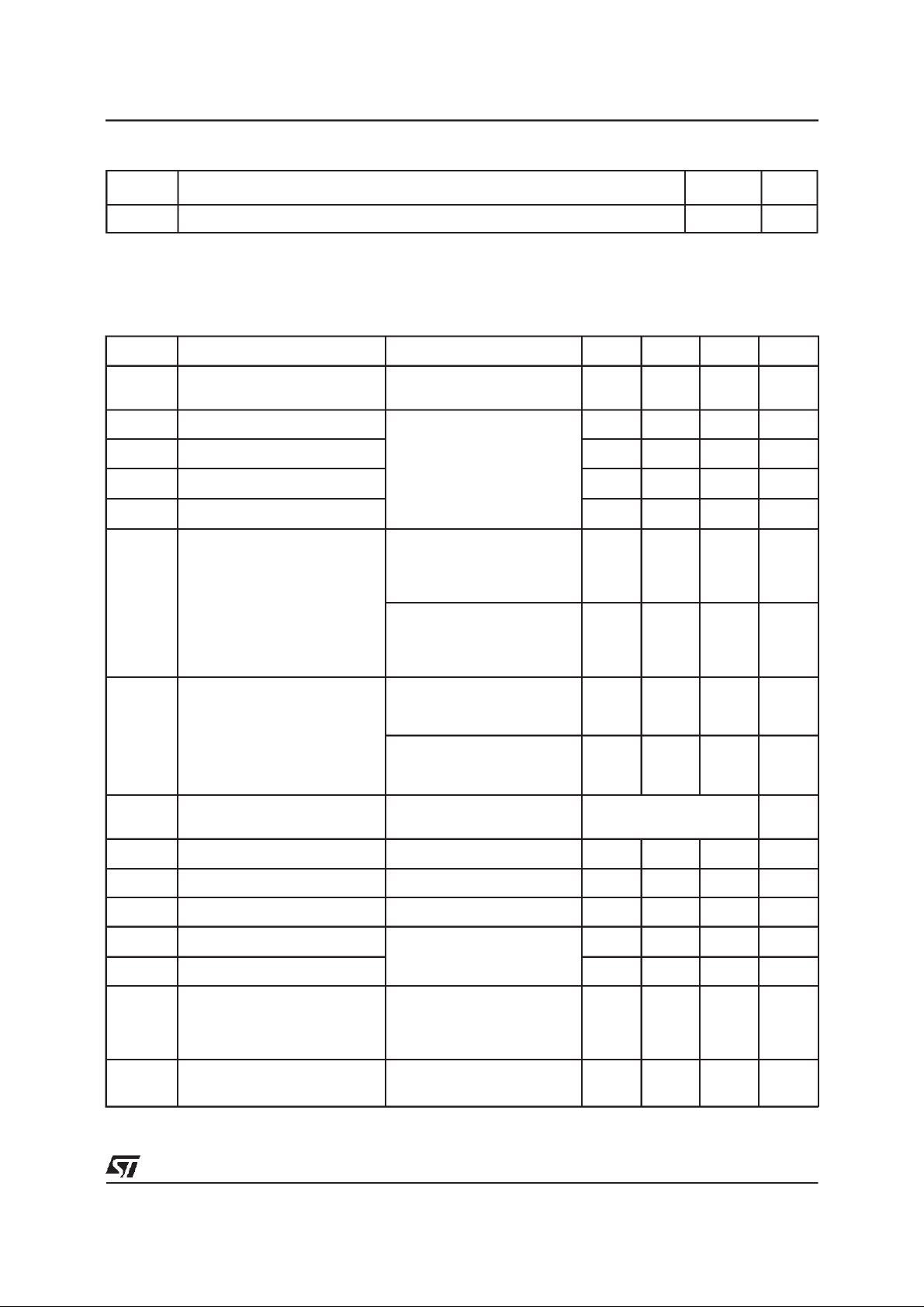
ABSOLUTEMAXIMUM RATINGS
Symbol Parameter Value Unit
V
P
T
stg,Tj
V
V
I
Supply voltage ±
s
Input voltage V
i
Differential input voltage ±
i
Output peak current (internally limited) 3.5 A
o
Powerdissipation at T
tot
Stoprage and junction temperature -40 to 150 °
case
=90°C
Pentawatt
TDA2030V
18 (36)
s
15
20 W
V
V
C
TYPICAL APPLICATION
June 1998
1/12

TDA2030
PIN CONNECTION(top view)
+V
S
OUTPUT
-V
S
INVERTING INPUT
NON INVERTING INPUT
TESTCIRCUIT
2/12
TDA2030
THERMAL DATA
Symbol Parameter Value Unit
R
th j-case
ELECTRICALCHARACTERISTICS
Thermal resistance junction-case max 3 °
(Referto the test circuit, V
=±14V , T
s
=25°C unless otherwise
amb
specified)for single Supply referto fig. 15 Vs= 28V
Symbol Parameter Test conditions Min. Typ. Max. Unit
V
I
I
V
I
os
P
Supply voltage
s
Quiescent drain current
d
Input bias current 0.2 2
b
V
= ± 18V (Vs = 36V)
Input offset voltage ±
os
s
Input offset current
o
Output power
d = 0.5% G
f = 40 to 15,000 Hz
R
=4
Ω
L
R
=8
Ω
L
d = 10%
f = 1 KHz
R
=4Ω
L
R
=8
Ω
L
=30dB
v
G
=30dB
v
± 6
12
12
8
40 60 mA
± 20 ± 200
14
9
18
11
± 18
36
2
20
±
C/W
V
A
µ
mV
nA
W
W
W
W
d Distortion
B Power Bandwidth
(-3 dB)
R
G
G
e
i
Input resistance (pin 1) 0.5 5
i
Voltagegain (open loop) 90 dB
v
Voltagegain (closed loop) f = 1 kHz 29.5 30 30.5 dB
v
Input noise voltage
N
Input noise current 80 200 pA
N
SVR Supply voltage rejection R
I
Drain current Po= 14W
d
P
= 0.1 to 12W
o
R
=4
Ω
L
f = 40 to 15,000 Hz 0.2 0.5 %
= 0.1 to 8W
P
o
R
=8Ω Gv=30dB
L
f = 40 to 15,000 Hz
G
=30dB
v
P
= 12W
o
Gv=30dB
=4
R
Ω
L
0.1 0.5 %
10 to 140,000 Hz
M
B = 22 Hz to 22 KHz
=4Ω Gv=30dB
L
R
=22k
Ω
g
= 0.5 V
V
f
ripple
P
ripple
o
= 100 Hz
=W
eff
R
L
R
L
=4
Ω
=8Ω
40 50 dB
310µ
900
500
mA
mA
Ω
V
3/12
TDA2030
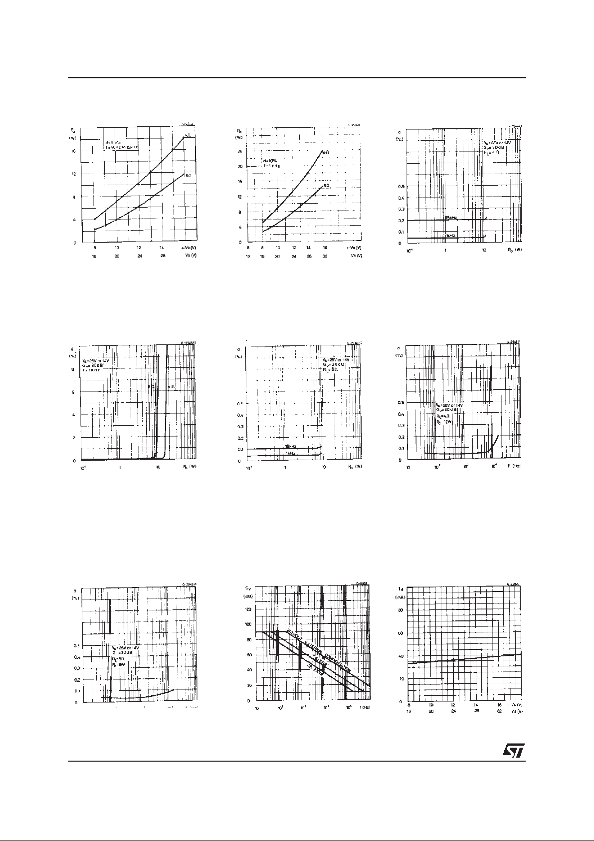
Figure 1. Output power vs.
supply voltage
Figure 4. Distortion vs.
output power
Figure 2. Output power vs.
supplyvoltage
Figure 5. Distortion vs.
output power
Figure 3. Distortion vs.
output power
Figure 6. Distortion vs.
frequency
Figure 7. Disto rtion vs .
frequency
4/12
Figure 8 . Frequency response with different values
of the rolloff capacitor C8
(see fig. 13)
Figure 9. Quiescent current
vs.supply voltage

TDA2030
Figure 10. Supply voltage
rejectionvs. voltagegain
Figure 11. Power dissipation andefficiencyvs.output
power
Figure 12. Maximum power
dissipation vs. supply voltage (sine wave operation)
APPLICATIONINFORMATION
Figure13.Typicalamplifier
with split power supply
Figure 14. P.C.board and component layoutfor
the circuitof fig. 13 (1 : 1 scale)
5/12

TDA2030
APPLICATION INFORMATION (continued)
Figure15.Typicalamplifier
with single powersupply
Figure 16. P.C.board and component layoutfor
the circuitof fig. 15 (1 : 1 scale)
Figure17. Bridge amplifierconfigurationwith split power supply (P
6/12
= 28W,Vs= ±14V)
o

PRACTICAL CONSIDERATIONS
TDA2030
Printedcircuit board
The layoutshown in Fig.16 should be adopted by
the designers. If different layouts are used, the
ground points of input 1 and input 2 must be well
decoupled from the ground return of the output in
which a high current flows.
Assemblysuggestion
No electri cal isolat ion is n eeded between the
Component
R1
R2
R3
R4
Recomm.
value
22 k
Ω Closed loop gain
680 Ω Closedloop gain
22 k
Ω
1
Ω Frequency stability Danger of osccilat. at
setting
setting
Non inverting input
biasing
Purpose
packageandthe heatsinkwithsinglesupplyvoltage
configuration.
Applicationsuggestions
The recommendedvalues of the components are
thoseshown on applicationcircuit of fig.13.
Different values can be used. The following table
can help the designer.
Larger than
recommended value
Increase of gain Decrease of gain (*)
Decrease of gain (*) Increase of gain
Increase of input
impedance
high frequencies
with induct.loads
Smaller than
recommended value
Decrease of input
impedance
R5 ≅
C1
C2
C3,C4
C5,C6
C7 0.22µF Frequency stability Danger of oscillation
C8
D1, D2 1N4001 Toprotect the deviceagainst output voltage spikes
(*) Closed loop gain must be higher than 24dB
100µF
≅
3R2
1µF
22µF
0.1 µF
1
2
π BR1
Upper frequency
cutoff
Input DC
decoupling
Inverting DC
decoupling
Supply voltage
bypass
Supply voltage
bypass
Upper frequency
cutoff
Poor high frequencies
attenuation
Smaller bandwidth Larger bandwidth
Danger of
oscillation
Increase of low
frequencies cutoff
Increase of low
frequencies cutoff
Danger of
oscillation
Danger of
oscillation
7/12

TDA2030
SINGLESUPPLY APPLICATION
Component
R1
R2
R3
R4
R
A/RB
C1
C2
C3
C5
C7 0.22µF Frequency stability Danger of oscillation
Recomm.
value
150 kΩ
4.7 k
100 k
1
Ω Frequency stability Danger of osccilat.at
100 k
1µF
22µF
0.1 µF
100µF
Closed loop gain
setting
Closed loop gain
Ω
setting
Ω Non inverting input
biasing
Non inverting input Biasing Power Consumption
Ω
Input DC
decoupling
Inverting DC
decoupling
Supply voltage
bypass
Supply voltage
bypass
Purpose
Larger than
recommended value
Increase ofgain Decrease of gain (*)
Decrease of gain (*) Increase of gain
Increase ofinput
impedance
high frequencies
with induct.loads
Smaller than
recommended value
Decrease of input
impedance
Increase of low
frequencies cutoff
Increase of low
frequencies cutoff
Danger of
oscillation
Danger of
oscillation
C8
D1, D2 1N4001 Toprotect the deviceagainst output voltage spikes
(*) Closed loop gain must be higher than 24dB
≅
1
2
π BR1
Upper frequency
cutoff
Smaller bandwidth Larger bandwidth
8/12

SHORTCIRCUIT PROTECTION
TDA2030
TheTDA2030hasan originalcircuitwhichlimitsthe
currentof the outputtransistors.Fig.18 showsthat
the maximum output current is a function of the
collector emitter voltage;hence the output transistors work within their safe operating area (Fig. 2).
This functioncan thereforebe consideredas being
Fig ure 18 . Max imum
output current vs.
voltage [V
CEsat
] across
each output transistor
peak power limiting rather than simple current limiting.
It reduces the possibilitythat thedevicegets damaged during an accidental short circuit from AC
output to ground.
Figure 19. Safe operating area and
collector characteristics of the
protectedpowertransistor
THERMAL SHUT-DOWN
The presenceof a thermallimitingcircuit offersthe
following advantages:
1. An overload on the output (even if it is permanent),oranabovelimitambienttemperaturecan
be easily supported since the T
cannot be
j
higherthan 150°C.
2. Theheatsinkcan havea smallerfactorof safety
compared with that of a conventional circuit.
Thereis no possibilityof device damagedue to
high junction temperature.If for any reason, the
junctiontemperatureincreasesup to 150°C,the
thermal shut-down simply reduces the power
dissipationat the current consumption.
The maximum allowable power dissipation dependsuponthe size of theexternalheatsink(i.e.its
thermal resistance); fig. 22 shows this dissipable
power as a function of ambient temperature for
differentthermal resistance.
9/12

TDA2030
Figure 20. Output power and
drai n c urrent vs. case
temperature(R
=4Ω)
L
Figure23. Example of heat-sink
Figure21. Output power and
drain current vs. case
temperature(RL=8Ω)
Dimension: suggestion.
The following table shows the length that
theheatsinkin fig.23musthaveforseveral
valuesof P
tot
Figure 22. Maximum
allowable power dissipation
vs.ambient temperature
and Rth.
Ptot (W) 12 8 6
Length of heatsink
Rth of heatsink
(°C/W)
(mm)
60 40 30
4.2 6.2 8.3
10/12

PENTAWATT PACKAGE MECHANICAL DATA
TDA2030
DIM.
mm inch
MIN. TYP. MAX. MIN. TYP. MAX.
A 4.8 0.189
C 1.37 0.054
D 2.4 2.8 0.094 0.110
D1 1.2 1.35 0.047 0.053
E 0.35 0.55 0.014 0.022
E1 0.76 1.19 0.030 0.047
F 0.8 1.05 0.031 0.041
F1 1 1.4 0.039 0.055
G 3.2 3.4 3.6 0.126 0.134 0.142
G1 6.6 6.8 7 0.260 0.268 0.276
H2 10.4 0.409
H3 10.05 10.4 0.396 0.409
L 17.55 17.85 18.15 0.691 0.703 0.715
L1 15.55 15.75 15.95 0.612 0.620 0.628
L2 21.2 21.4 21.6 0.831 0.843 0.850
L3 22.3 22.5 22.7 0.878 0.886 0.894
L4 1.29 0.051
L5 2.6 3 0.102 0.118
L6 15.1 15.8 0.594 0.622
L7 6 6.6 0.236 0.260
L9 0.2 0.008
M 4.23 4.5 4.75 0.167 0.177 0.187
M1 3.75 4 4.25 0.148 0.157 0.167
V4 40° (typ.)
Dia 3.65 3.85 0.144 0.152
H3
L
L1
VV
A
B
C
L5
H1
Dia.
L7
L8
V1
R
D
D1
L6
L2
L3
V3
R
R
V4
V4
F1
RESIN BETWEEN
LEADS
F
H2
E
M1
M
GG1
V4
L9
VV
H2
F
E1
E
11/12

TDA2030
Informationfurnished is believedto be accurate andreliable.However, STMicroelectronics assumes no responsibility for the consequences of
use ofsuch information nor for any infringement of patents or other rights of third parties which may result from its use.No license is granted
by implication or otherwise under any patent or patent rights of STMicroelectronics. Specification mentioned in this publication are subjectto
change without notice. This publication supersedes and replaces all information previously supplied. STMicroelectronics products are not
authorized for use as critical components in lifesupport devices or systems withoutexpress written approval of STMicroelectronics.
The ST logois a registered trademark of STMicroelectronics
1998 STMicroelectronics – Printed in Italy – All Rights Reserved
STMicroelectronics GROUP OF COMPANIES
Australia - Brazil - Canada - China- France - Germany - Italy - Japan - Korea - Malaysia - Malta - Mexico - Morocco - The Netherlands -
Singapore - Spain - Sweden - Switzerland - Taiwan- Thailand- United Kingdom - U.S.A.
12/12
 Loading...