

Page 1
.WIDESUPPLYVOLTAGERANGE (3 to 36V)
.SINGLEOR SPLITSUPPLYOPERATION
.VERYLOW CURRENT CONSUMPTION
(0.8mA)
.VERYLOW DISTORTION
.NOPOP-NOISE
DESC RIP TI ON
The TDA2320Ais a stereoclass A preamplifierintended for application in portablecassette players
and high qualityaudio systems.
The TDA2320Ais a monolithicintegratedcircuit in
a 8leadplastic dip.
STEREOAMPLIFIER
(Plastic Package)
ORDER CODES
Part Number
TDA2320A -40
TDA2320A
N
DIP8
Temperature
Range
o
C, +105oC •
Package
N
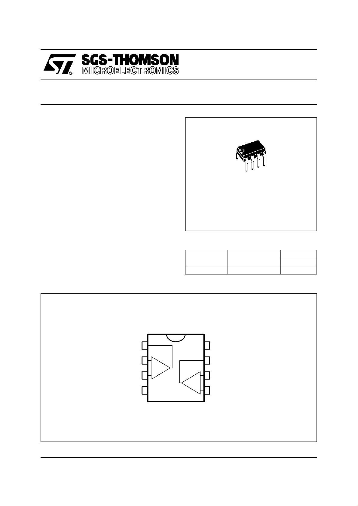
PI N CO NNECT IONS (top view)
Output 1
Inverting Input 1
Non-inve rting Input 1
GND
October 1997
1
2
-
+
3
45
-
+
8
V
CC
7
Output 2
6
Inverting Input 2
Non-inverting Input 2
1/12
Page 2
TDA2320A
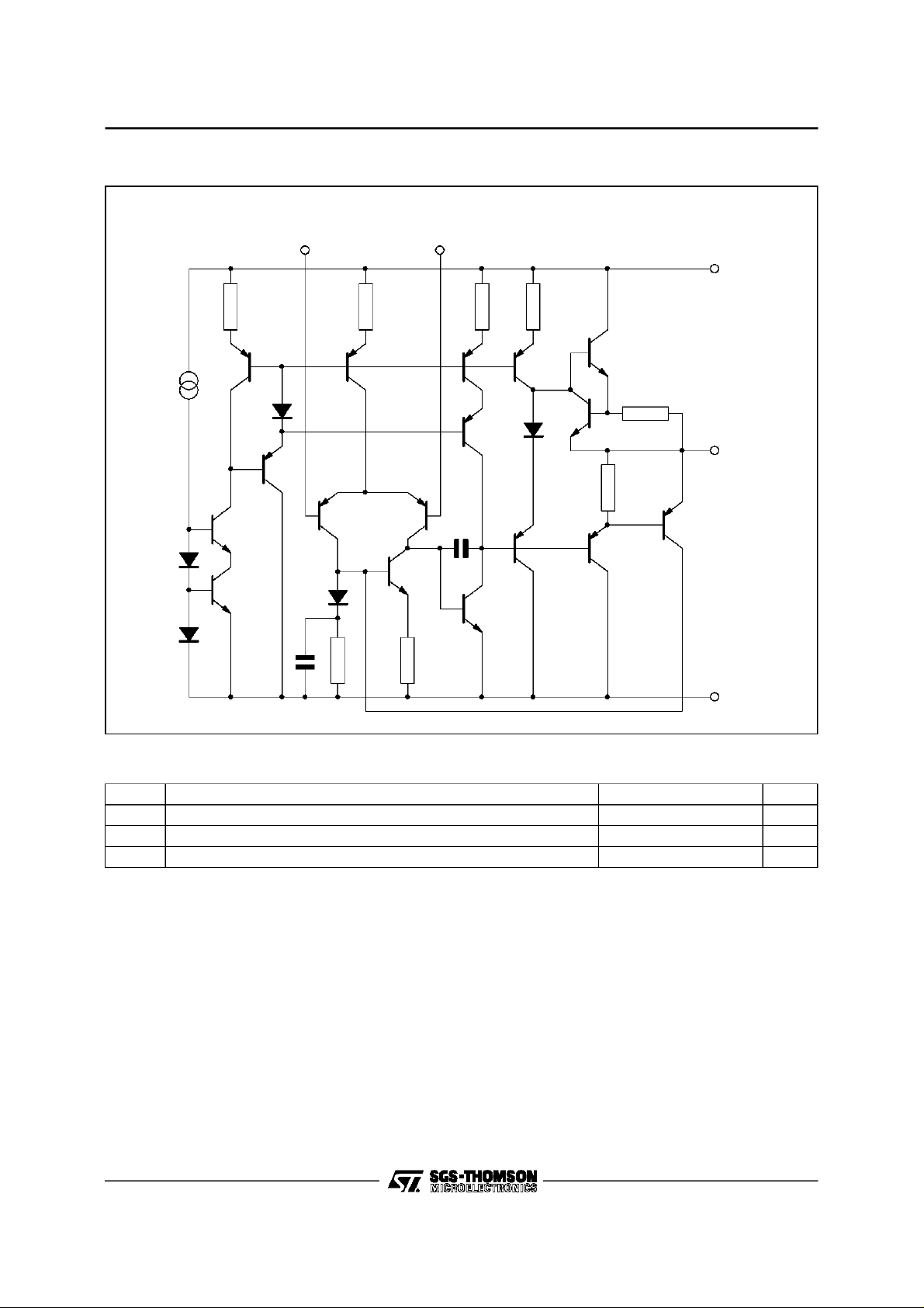
SCHE MATIC DIAGRAM (1/2 TDA2320A)
D1
D2
Inverting
Input
R1 R3
Q3
D3
Q4
Q5
Q2
Q1
D4
C1
Q6
Non-inverting
Input
Q7
C2
Q17
R4R2
Q8
Q9
Q10
R5
D5
Q11
Q12
R6
Q14
Q13
Q15
R8
R7
Q16
V
CC
Output
GND
ABSOLUTE MAXIMUM RATINGS
Symbol Parameter Value Unit
V
P
T
stg,Tj
Supply Voltage 36 V
CC
Total Power Dissipation at T
tot
Storage and Junction Temperature –40 to 150
=70oC 400 mW
amb
o
C
2/12
Page 3
TDA2320A
ELECTRICAL CHARACTERISTICS
= 15V, T
V
CC
Symbol Parameter Min. Typ. Max. Unit
V
CC
I
CC
I
ib
V
io
I
io
A
vd
V
OPP
GBP Gain-bandwidth Product
FBP Power Bandwidth (*)
SR Slew Rate (*) 1 1.6 V/µs
THD Distortion (V
e
n
V
O1/V02
SVR Supply Voltage Rejection Ratio(**)
(*) Test circuit of figure 1
(**) Test circuit of figure 2
=25oC (unless otherwise specified) (refer to the test circuits)
amb
Supply Voltage (*) 3 36 V
Supply Current (*) 0.8 2 mA
Input Bias Current 150 500 nA
Input Offset Voltage
≤ 10kΩ 15
R
s
Input Offset Current 10 50 nA
Open Loop Voltage Gain
= 15V f = 333Hz
V
CC
= 4.5V f = 1kHz
V
CC
f = 1kHz
f = 10kHz
80
70
50
70
Output Voltage Swing (f = 1kHz, RL= 600Ω) (*)
V
V
CC
CC
= 15V
= 4.5V
13
2.5
f = 20kHz 1.5 2.5
=5VPP, THD = 1% 40 70
V
o
= 2V, AV= 20dB) (*)
o
f = 1kHz
f = 10kHz
0.03
0.08
Equivalent Input Noise Voltage (**)
Curve A R
B = 22Hz to 22kHz R
f = 1kHz R
R
R
R
R
s
s
s
s
s
s
s
=50Ω
= 600Ω
=5kΩ
=50Ω
= 600Ω
=5kΩ
= 600Ω
1
1.1
1.5
1.3
1.5
2
9
1.4
Channel Separation (**)
f = 1kHz 100
f = 100Hz 80
mV
dB
V
MHz
kHz
%
µV
nV√Hz
dB
dB
3/12
Page 4
TDA2320A
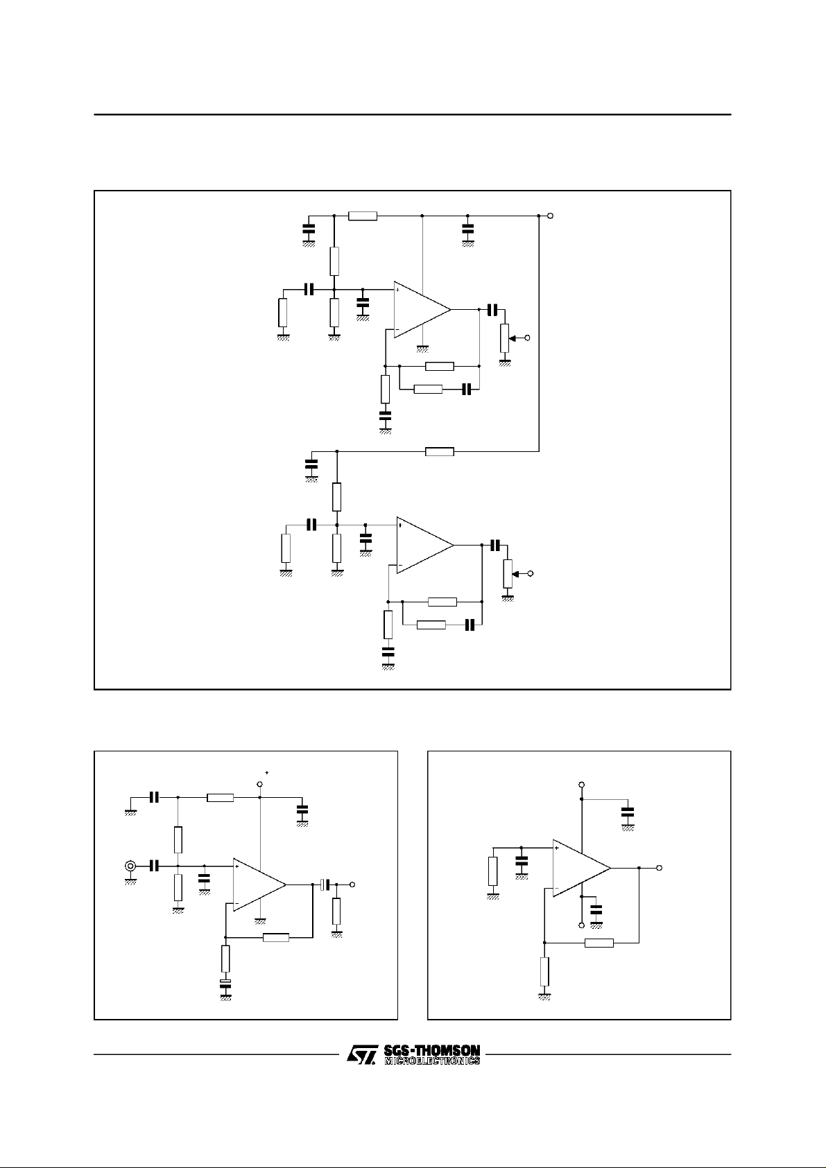
TYP ICAL APPLI C ATION
STEREO PR EAMPLIFIER FOR CASSETTE PLAYERS
TAPE
HEAD
TAPE
HEAD
0.3mV
0.3mV
22µF
22µF
4.7µF
100k
4.7µF
100kΩ
18kΩ
0.1µF
82kΩ
5
8
1/2
220pF
150Ω
Ω
150Ω
220pF
TDA2320A
6
22µF
3
TDA2320A
2
1/2
4
15kΩ
15k
180kΩ
18kΩ
180kΩ
Ω
Ω
82k
7
1
1µF
20kΩ
10nF
1µF
20kΩ
10nF
V
CC
TES T CIRCUITS
Figure 1
22µF
82k
0.22µF
IN
100kΩ
4/12
22µF
Figure 2
V
18kΩ
Ω
220pF
CC
1/2
TDA2320A
150Ω
47µF
0.1µF
R
1µF
OUT
Ω
22k
Rx
s
220pF
+7.5V
1/2
TDA2320A
-7.5V
33Ω
0.1µF
OUT
0.1µF
3.3kΩ
Page 5

TDA2320A
Figure 3 : Sup ply Curren t ve rsus Sup p ly
Voltage
Figure 5 : Output Voltage Swing versus
Load Resistance
Figure 4 : Supply Current versus Ambient
Temperature
Figure6: Power Bandwidth
Figure 7 : Tota l Harmonic Distortion
versusOutput Voltage
Figure8: Total Input Noise v ersus Source
Resistance
5/12
Page 6

TDA2320A
Figure 9 : Noise Density versus
Frequency
Figure 11 : Tape Preamplifier Frequency
Figure10:RIAA Preamplifier Response
6/12
Page 7

APPL ICATION INFORMATION
Figure 12 :Stereo RIAA Preamplifier
22µF
C3
22µF
4.7µF
120kΩ
4.7µF
120k
C1
R2
C4
C2
R4
Ω
IN (L)
IN (R)
18kΩ
R1
100k
C5
R3
100kΩ
C6
R5
Ω
R7
820
10µF
R8
820Ω
10µF
100pF
Ω
100pF
5
TDA2320A
6
C7
3
TDA2320A
2
C8
TDA2320A
1µF
1µF
+15V
OUT (L)
OUT (R)
0.1µFC13
8
1/2
4
3.3nFC9
R10
Ω
22k
R6
18kΩ
1/2
3.3nFC11
R12
Ω
22k
7
1
220kΩ
15nF
220kΩ
15nF
R9
R11
C10
C12
C14
C15
R13
1kΩ
R14
1kΩ
Figure 13 :P.C. Board and Components layout of the Circuit of figure 1 2
7/12
Page 8

TDA2320A
Figure 14 :Second Order 2kHz Butterworth
Crossover Filter for Hi-Fi Act ive
Boxes
+15V
100nF
12nF
6
8
-15V
0.47µF
7
4
100nF
1
5kΩ
5.6kΩ
0.1µF
5kΩ
5.6kΩ
TO
WOOFER
AMPLIFIER
TO
TWEETER
AMPLIFIER
1/2
0.22µF
10kΩ10k
f = 2kHz
c
10kΩ
IN
5.6nF 5.6nF
Ω
5.6nF
22kΩ
TDA2320A
5
2
TDA2320A
3
1/2
Figure15:Third Order 2.8kHz Bessel
Crossov e r Filter for Hi-Fi
Actives Boxes
+15V
100nF
C3
6.8nF
INPUT
C1
0.22µF
4.7nF
R1
12kΩR212kΩ
C2
4.7nF
f = 2.8kHz
c
C6
R5
Ω
12k
C7
4.7nF
R3
12kΩ
R6
8.2k Ω
4.7nF
C4
1.2nF
C8
R7
47k
6
1/2
TDA2320A
5
2
1/2
TDA2320A
3
Ω
-15V
C5
8
0.47µF
7
100nF
1
5kΩ
R4
5.6kΩ
0.1µF
5kΩ
R8
5.6kΩ
P1
C9
P2
4
WOOFER
AMPLIFIER
TWEETER
AMPLIFIER
Figure 16 : Frequency Response
(circuit of figure 14)
Figure17:Frequency Response
(circuit of figure 15)
8/12
Page 9

Figure 18 :200Hz t o 2kHz Active Bandpass Filter for MidrangeSpeakers
V
CC
TDA2320A
10kΩ
56nF 56nF
IN
2
3
22kΩ
Figure 19 :Subsonic Filter
C
V
in
C
22kΩ
1/2
TDA2320A
V
CC
10k Ω
0.3µF
1
0.1µF
3
TDA2320A
2
-
1/2
12k
10nF
Ω
12k
6.8nF
Ω
12k
Ω
6
1/2
TDA2320A
5
1.8nF
7
0.47µF
5kΩ
5.6kΩ
fc(Hz) C (µF)
15
1
V
out
22
30
55
100
0.68
0.47
0.33
0.22
0.1
Figure 2 0 :High-cut Filter
V
in
10kΩ
10kΩ
C1
C2
3
1/2
TDA2320A
2
-
(kHz) C1 (nF) C2 (nF)
f
c
3
1
V
out
5
10
15
3.9
2.2
1.2
0.68
6.8
4.7
2.2
1.5
9/12
Page 10

TDA2320A
Figure 21 :Fifth Order 3 .4kHz Low-pass Butterworth Filter
C2
.
.
.
1
2Π f
1
2Π f
1
2Π f
R1
= 6.33nF
c
= 1.97nF
c
= 8.20nF
c
R
i
C
i
1st order 2nd order 3rd order
Forf
=3.4kHzand Ri=R1 =R2 = R3 =R4 = 10kΩ, weobtain :
c
C1 = 1.354.
C1 = 0.421.
C2 = 1.753.
1
R
1
R
1
R
R2
C1
3
1/2
TDA2320A
2
-
1
R3
C3 = 0.309.
C4 = 3.325.
R4
1
1
.
R
2Π f
1
1
.
R
2Π f
The attenuationof thefilter is 30dB at 6.8kHz and
betterthan 60dB at 15kHz.
Figure 22 :Sixth-pole 355Hz Low-p ass Filter (Chebychev type)
C4
5
C3
6
= 1.45nF
c
= 15.14nF
c
1/2
TDA2320A
-
7
6
-
1/2
TDA
7
161nF
0.47µF
56k
Ω
2
3
-
1/2
TDA
2320A
86.1nF
5
2320A
10kΩ
Ω
10k
1
Thisis a6-poleChebychevtypewith±0.25dBripple
inthepassband.A decouplingstageisusedtoavoid
the influence of the input impedance of the filter’s
characteristics.
10/12
6
2
-
10k
1/2
1
TDA
16.3nF
3
2320A
220nF
10kΩ
Ω
10k
10kΩ
Ω
5
3.54nF
The attenuation is about 55dB at 710Hz and
reaches80dBat 1065Hz.The in bandattenuation
islimited inpractice tothe±0.25dBripple anddoes
not exceed1/2dB at 0.9f
.
c
-
1/2
TDA
2320A
7
60nF
Page 11

Figure 23 :Three Ban d Tone Control
TDA2320A
+15V
100nF
0.22µF
IN
56kΩ
3
1/2
TDA2320A
2
-15V
6
1
4
100nF
Figure 2 4 :Frequen cy Respon se of the
Circuit of figu re 2 3
11kΩ
1.8kΩ 500kΩ
100kΩ
100kΩ3.6kΩ
47nF
47nF
22nF
4.7nF
BASS
11kΩ
MIDRANGE
3.6kΩ
TREBLE
1.8kΩ
6
1/2
TDA2320A
5
A:allcontrolsflat
B:bass& trebleboost,mid flat
11kΩ
7
OUT
C:bass& treblecut,mid flat
D:mid boost,bass & trebleflat
E:mid cut,basstrebleflat
11/12
Page 12

TDA2320A
PACKAGE MECHANI CAL DATA
8 PINS -PLASTIC DIP
Dimensions
Min. Typ. Max. Min. Typ. Max.
Millimeters Inches
A 3.32 0.131
a1 0.51 0.020
B 1.15 1.65 0.045 0.065
b 0.356 0.55 0.014 0.022
b1 0.204 0.304 0.008 0.012
D 10.92 0.430
E 7.95 9.75 0.313 0.384
e 2.54 0.100
e3 7.62 0.300
e4 7.62 0.300
F 6.6 0260
i 5.08 0.200
L 3.18 3.81 0.125 0.150
Z 1.52 0.060
Information furnished is believed to be accurate and reliable. However, SGS-THOMSON Microelectronics assumes no responsibility for the consequences of use of such information nor for any infringement of patents or other rights of third parties which
may result from its use. No license is granted by implication or otherwise under any patent or patent rights of SGS-THOMSON
Microelectronics. Specifications mentioned in this publicationare subject to change without notice. This publication supersedes
and replaces all information previously supplied. SGS-THOMSON Microelectronics products are not authorized for use as critical
components in life support devices or systems without express written approvalof SGS-THOMSON Microelectronics.
PM-DIP8.EPS
DIP8.TBL
1997 SGS-THOMSON Microelectronics – Printed in Italy – All Rights Reserved
SGS-THOMSON Microelectronics GROUP OF COMPANIES
Australia - Brazil- Canada - China - France - Germany - Hong Kong - Italy- Japan - Korea - Malaysia - Malta - Morocco
The Netherlands - Singapore - Spain - Sweden - Switzerland - Taiwan - Thailand - United Kingdom- U.S.A.
12/12
ORDER CODE :
 Loading...