

.
SYNCHRONISATION CIRCUIT
.
ESD PROTECTED
.
PRECISION OSCILLATOR AND RAMP
GENERATOR
.
POWER OUTPUT AMPLIFIER WITH HIGH
CURRENT CAPABILITY
.
FLYBACK GENERATOR
.
VOLTAGE REGULATOR
.
PRECISION BLANKING PULSE GENERATOR
.
THERMAL SHUT DOWN PROTECTION
.
CRT SCREEN PROTECTION CIRCUIT
WHICH BLANKS THE BEAM CURRENT IN
THE EVENT OF LOSS OF VERTICAL DEFLECTION CURRENT
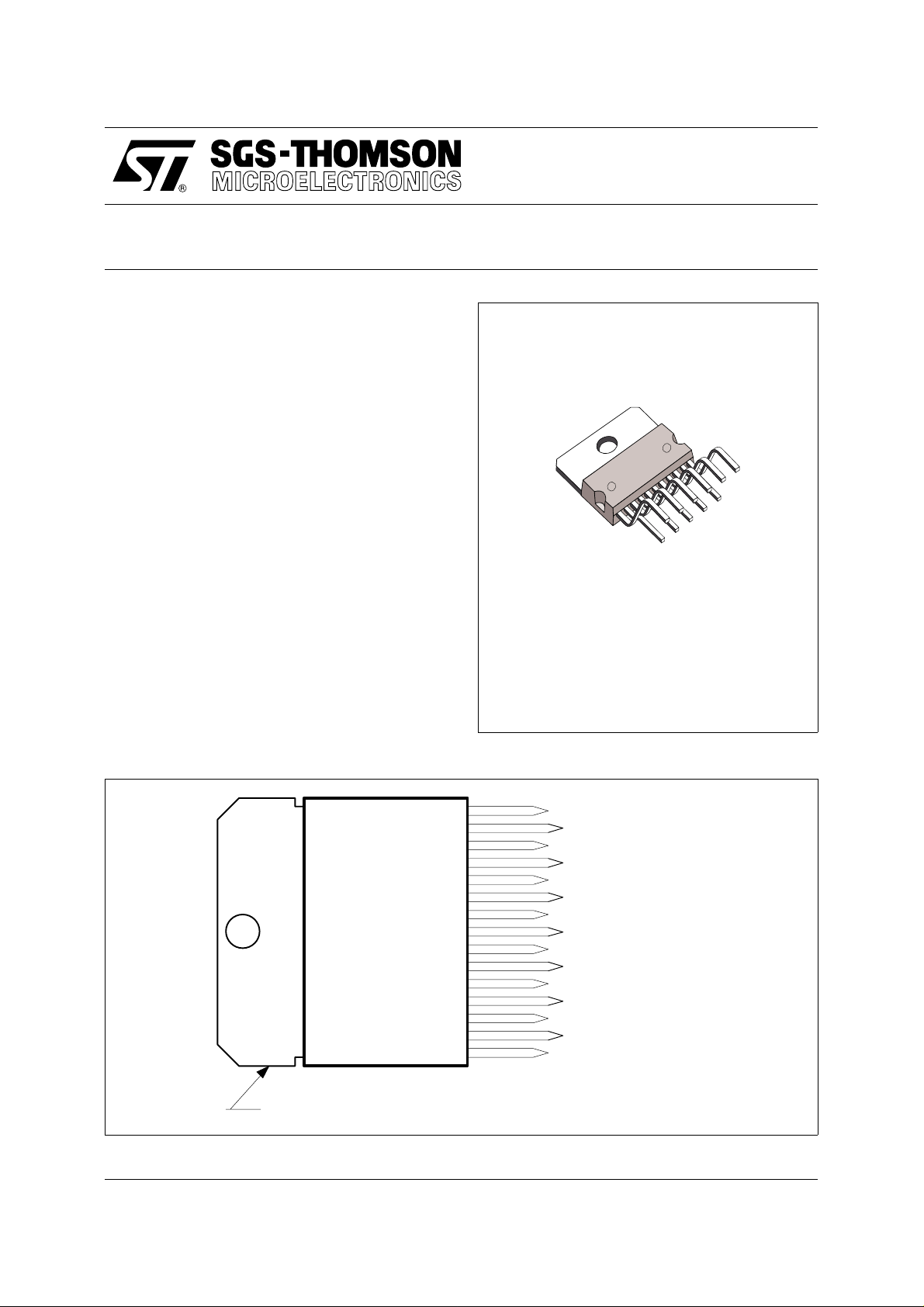
TDA1675A
VERTICAL DEFLECTION CIRC UIT
MULTIWATT 15
(Plastic Package)
DESCRIPTION
The TDA1675A is a monolithic integrated circ uit i n
15-lead Multiwatt
and very efficient vertical def lection circuit intended
for direct drive of the yoke of 1 10
tubes. It offers a wide range of applications also in
portable CTVs, B&W TVs, monitors and displays.
PIN CONNECTIONS (top view)
®
package. It is a full performance
o
colour TV picture
15
14
13
12
11
10
ORDER CODE : TDA1675A
FLYBACK
SUPPLY
BLANKING OUTPUT
AMPLIFIER INPUT (-)
AMPLIFIER INPUT (+)
RAMP OUTPUT
9
8
7
6
5
4
3
2
1
RAMP GENERATOR
GROUND
HEIGHT ADJUSTMENT
OSCILLATOR
SYNC. INPUT
OSCILLATOR
OSCILLATOR
AMPLIFIER SUPPLY
AMPLIFIER OUTPUT
September 1993
Tab connected to Pin 8
1675A-01.EPS
1/11
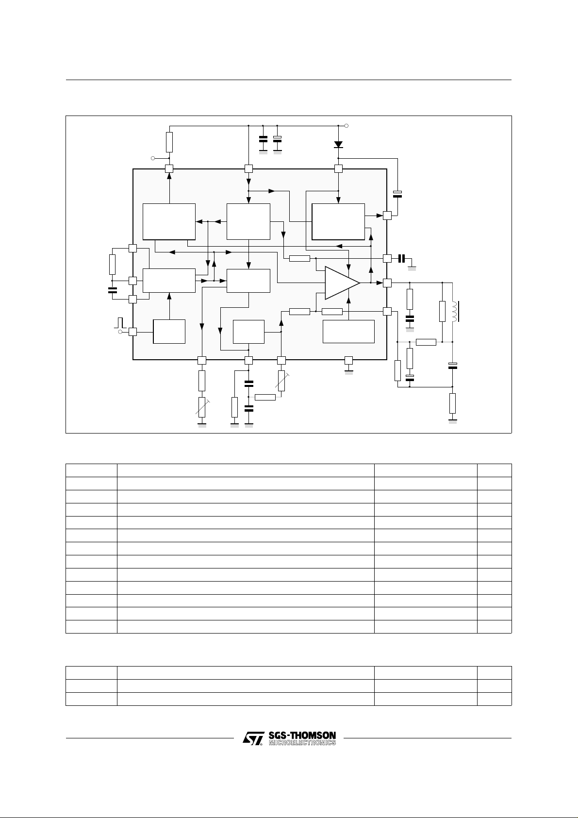
TDA1675A
BLOCK DIAGRAM
BLANKING
OUT
6
R
o
4
C
o
3
7
SYNC.
+
13 2
BLANK
GENERATOR
AND CRT
PROTECTION
OSCILLATOR
SYNC.
14
VOLTAGE
REGULATOR
RAMP
GENERATOR
BUFFER
STAGE
R3
CLOCK
PULSE
R1 R2
FLYBACK
GENERATOR
+
POWER
AMP.
-
THERMAL
PROTECTION
+V
S
+
C
f
15
11
Ly
Ry
Iy
e
YOKE
12
1
R
R
a
+
R
f
HEIGHT
R
7
9
R
d
10
C
a
LIN
C
b
8
R
b
c
+
C
c
ABSOL UTE MAX IM UM RAT INGS
Symbol Parameter Value Unit
V
S
, V
V
1
V
5
, V
V
11
V
13
I
O
I
O
I
O
I
15
I
15
P
tot
, T
T
stg
Supply Voltage at Pin 14 35 V
Flyback Peak Voltage 65 V
2
Sync. Input Voltage 20 V
Power Amplifier Input Voltage VS - 10 V
12
Voltage at Pin 13 V
S
Output Current (non repetitive) at t = 2ms 3 A
Output Peak Current at f = 50Hz t > 10µs2A
Output Peak Current at f = 50Hz t ≤ 10 µs 3.5 A
Pin 15 Peak-to-peak Flyback Current at f = 50Hz, tfly ≤ 1.5ms 3 A
Pin 15 D.C. Current at V1 < V
Maximum Power Dissipation at T
Storage and Junction Temperature - 40, + 150
j
14
≤ 60oC30W
case
100 mA
1675A-02.EPS
o
C
1675A-01.TBL
THERMAL DATA
Symbol Parameter Value Unit
2/11
R
R
TH(j-c)
TH(j-a)
Thermal Resistance Junction-case
Thermal Resistance Junction-ambient
Max. 3
Max. 40
o
C/W
o
C/W
1675A-02.TBL
TDA1675A
DC ELECTRICAL CHARACTE RIS T ICS (VS = 35V, T
= 25oC, unless otherwise specified)
amb
Symbol Parameter Test conditions Min. Typ. Max. Unit Fig.
I
Pin 2 quiescent current I1 = 0 16 36 mA 1b
2
- I
- I
∆I
I
V
V
V
V
V
∆V
∆V
V
V
V
Ramp generator bias current V9 = 0 0.02 1 µA1b
9
Ramp generator current V9 = 0 ; - I7 = 20µA 18.5 20 21.5 µA1b
9
9
Ramp generator non linearity ∆V9 = 0 to 15V, - I7 = 20µA 0.2 1 % 1b
I
9
Pin 14 quiescent current 25 45 mA 1b
14
Quiescent output voltage VS = 35V, Ra = 2.2kΩ, Rb = 1kΩ
1
Output saturation voltage to ground I1 = 1.2A, 1 1.4 V 1c
1L
Output saturation voltage to supply - I1 = 1.2A 1.6 2.2 V 1d
1H
Oscillator virtual ground 0.45 V 1b
4
Regulated voltage at pin 7 - I7 = 20µA 6.3 6.6 7 V 1b
7
7
Regulated voltage drift with supply
voltage
S
Amplifier input (+) reference voltage 4.1 4.4 4.7 V 1b
11
Blanking output saturation voltage I13 = 10 mA 0.35 0.5 V 1a
13
Pin 15 saturation voltage to ground I15 = 20 mA 1 1.5 V 1a
15
VS = 15V, Ra = 390Ω, Rb = 1kΩ
∆VS = 15 to 35V 1 2
16.4
6.9
17.8
7.5
19.5
8.1VV
mV
V
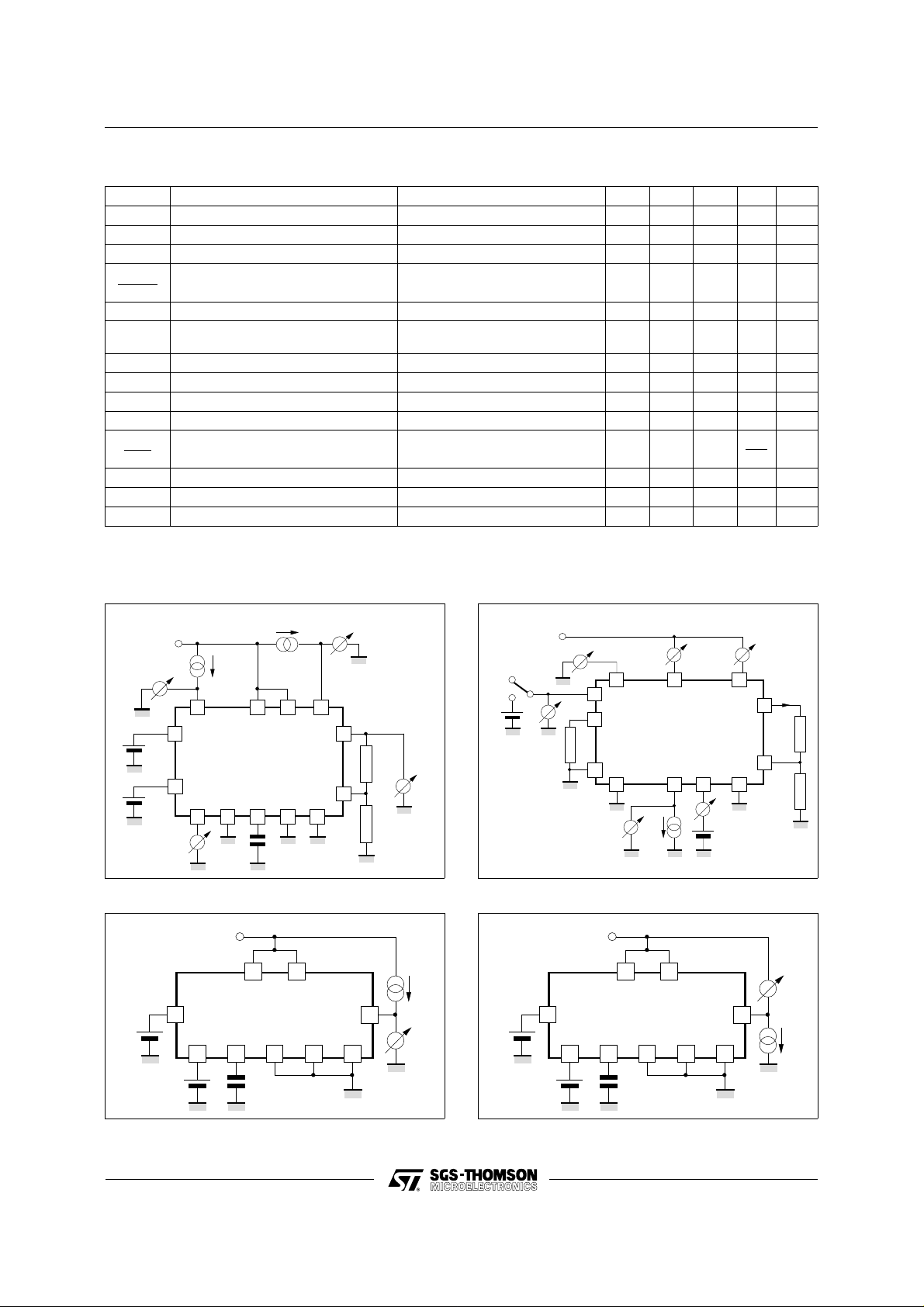
Figure 1 : DC Test Circuit.
Figure 1a
V
V
13
8V
1V
I
15
S
I
13
13
7
4
59 11 8 10
-I
9
0.1µF
2
14 15
V
15
1
R
a
V
12
R
1
b
Figure 1b
1675A-03.EPS
1V
V
S
V
11
A
B
V
4
75kΩ
I2+ I
1
11
4
4
3
5
V
7
2
97 810
-I
7
I
14
14
I
1
12
-I
9
V
9
1a
1b
1675A-03.TBL
1
22kΩ
47kΩ
1675A-04.EPS
Figure 1c
1V
V
4
12 5
8V
S
14
2
11 8
10
0.1µF
Figure 1d
V
S
14
2
+I
1
1
V
1L
1V
1675A-05.EPS
4
12 5
8V
11 8
10
0.1µF
V
1H
1
-I
1
1675A-06.EPS
3/11
TDA1675A
AC ELECTRICAL CHARACTE RIS TICS
(Refer to A.C. test circuit of fig. 2, T
Symbol Parameter Test conditions Min. Typ. Max. Unit
Supply Current IY = 2A
S
Sync Input Current Required to Sync 100 µA
I
5
Flyback Voltage Iy = 2App 50 V
1
Peak-to-peak Oscillator Sawtooth
3
Voltage
Start Scan Level of the Input Ramp 1.85 V
Flyback Time Iy = 2App 0.6 ms
Blanking Pulse Duration fo = 50Hz, Tj = 75oC
Free Running Frequency Ro = 7.5kΩ, Co = 330nF, Tj = 75oC
f
o
V
10TH(L)
t
t
BLANK
I
V
V
FLY
∆f Synchronization Range I
T
V
Junction Temperature for Thermal
j
Shut-down
Peak-to-peak Output Noise 35 mV
ON
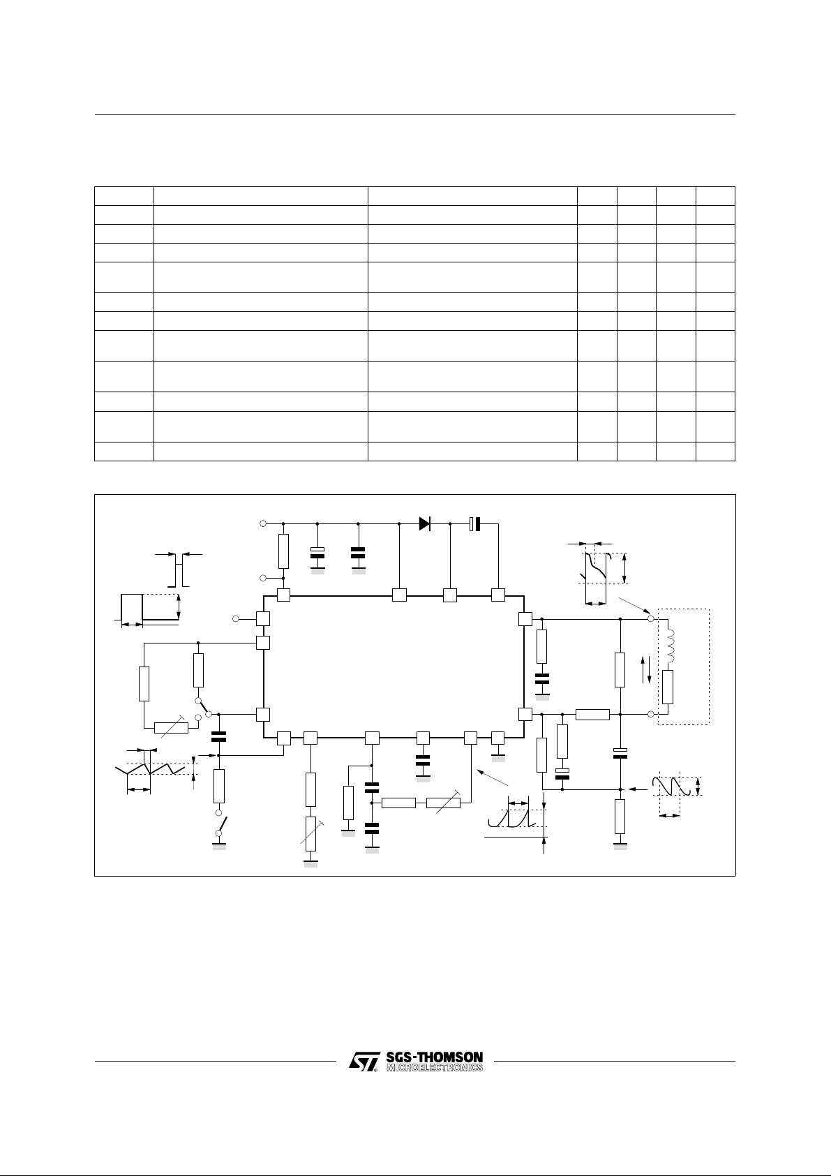
Figure 2 : A C Test Circuit
+V
S
t
4.7k
(FREQ.)
t
blank
Ω
Ω
4.7k
1/fo
100µA
t
sync.
blank
SYNC. IN
Ω
7.5k
A
B
C
V
SERVICE
SWITCH
o
3
BLANKING
OUT
S1 (R )
o
0.33µF
15kΩ
S2
2.4kΩ
13
5
6
4
3
220kΩ
HEIGHT
= 25oC, VS = 24V, f = 50Hz, unless otherwise specified)
amb
PP
I5 = 0
= 100µA
I
5
1.33 1.4
fo = 60Hz, Tj = 75oC
42 43.5
Ro = 6.2kΩ, Co = 330nF, Tj = 75oC
= 100µA, Tj = 75oC1416Hz
5
1N4001 220µF
tfI
y
0.1µF
1000µF
1/fo
GND
1/fo
1
2.2Ω
0.22µF
Ω
V
V
2.4k
120Ω
47µF
10
10thL
12
1kΩ
14 15
2
TDA 1675A
7 8
Ω
180k
9
0.1µF
560kΩ
0.1µF
LINEARITY
1011
0.1µF
100kΩ56kΩ
GND
295 mA
3.6
3.4
1.47 ms
1.17
46 Hz
52.5
145
V
1
I
Y
270Ω
2200µF
Ω
0.82
1/fo
R
f
YOKE
10mH
5.9Ω
V
V
ms
Hz
o
C
PP
1675A-04.TBL
R
I
f
y
1675A-07.EPS
4/11

TDA1675A
Figure 3 : Application Circuit for Small Scree 90o CTV Set (Ry = 15Ω ; Ly = 30 mH ; Iy = 0.82 APP)
1N4001D1220µF - 35V
+V
S
R3
Ω
10k
BLANKING
OUT
SYNC.
PULSE
IN
0.1µF
C1
R1
4.7kΩ
R
7.5k
1%
330nF
5%
C
o
R2
15kΩ
SERVICE
SWITCH
* The value depends on the characteristics of the CRT. The value shown is indicative only.
S1
13
5
6
o
Ω
4
3
150kΩ
HEIGHT
C2
35V
470µF
7 8
*
R4
390kΩ
RT1
100kΩ
C3
0.1µF
TDA 1675A
9
C5 0.1µF
*
R5
14 15
Ω
RT2
56k
R6
*
C6
0.1µF
0.1µF
100k
2
1011
Ω
C4
LINEARITY
1
C7 0.22µF
12
R7
910Ω
2%
R9
2.2Ω
120
R8
C8
R11
330Ω
Ω
2.4k
*
R10
2%
Ω
47µF
10V
5%
C9
1000µF
25V
R12
Ω
2.2
YOKE
1675A-08.EPS
TYPICAL PERFORMANCE
Symbol Parameter Value Unit
V
S
I
S
t
FLY
t
BLKG
f
O
* P
TOT
* R
TH(heatsink)
* Worst case condition.
Minimum supply voltage 25 V
Supply current 140 mA
Flyback time 0.7 ms
Banking time 1.4 ms
Free running frequency 43.5 Hz
Power dissipation 2.4 W
Thermal resistance of the heatsink
for T
for T
= 60oC and T
amb
= 60oC and T
amb
j max
j max
= 110oC
= 120oC
13
16
o
C/W
o
C/W
1675A-05.TBL
5/11

TDA1675A
Figure 4 : Application Circuit for 11 0o CTV Set (Ry = 9.6Ω ; Ly = 24.6 mH ; Iy = 1.2 APP)
1N4001D1220µF - 25V
14 15
Ω
56k
R6
*
C6
0.1µF
2
0.1µF
RT2
100k
C4
1011
LINEARITY
Ω
SYNC.
PULSE
IN
0.1µF
C1
BLANKING
OUT
R1
4.7kΩ
C
SERVICE
SWITCH
+V
S
R3
Ω
10k
13
5
6
R
o
7.5k
Ω
1%
4
330nF
5%
o
R2
15kΩ
S1
3
180kΩ
HEIGHT
C2
35V
470µF
7 8
*
R4
470kΩ
RT1
220kΩ
C3
0.1µF
TDA 1675A
9
C5 0.1µF
*
R5
* The value depends on the characteristics of the CRT. The value shown is indicative only.
1
C7 0.22µF
12
R7
1.2kΩ
2%
R9
2.2Ω
120
R8
C8
YOKE
R11
330Ω
Ω
2.4k
*
R10
2%
Ω
47µF
10V
C9
5%
1500µF
16V
R12
Ω
1.2
1675A-09.EPS
TYPICAL PE RF O RMANC E
Symbol Parameter Value Unit
V
S
I
S
t
FLY
t
BLKG
f
O
* P
TOT
* R
TH(heatsink)
* Worst case condition.
Minimum supply voltage 22.5 V
Supply current 185 mA
Flyback time 1 ms
Banking time 1.4 ms
Free running frequency 43.5 Hz
Power dissipation 2.7 W
Thermal resistance of the heatsink
for T amb = 60oC and T
for T
= 60oC and T
amb
j max
j max
= 110oC
= 120oC
11.5
14.5
o
C/W
o
C/W
1675A-06.TBL
6/11

Figure 5 : Application Circuit for 11 0o CTV Set (Ry = 5.9Ω ; Ly = 10 mH ; Iy = 1.95 APP)
TDA1675A
1N4001D1220µF - 25V
14 15
Ω
56k
R6
*
C6
0.1µF
2
0.1µF
RT2
100k
C4
1011
LINEARITY
Ω
SYNC.
PULSE
IN
0.1µF
C1
BLANKING
OUT
R1
4.7kΩ
C
SERVICE
SWITCH
+V
S
R3
Ω
10k
13
5
6
R
o
7.5k
Ω
1%
4
330nF
5%
o
R2
15kΩ
S1
3
180kΩ
HEIGHT
C2
35V
1000µF
7 8
*
R4
560kΩ
RT1
220kΩ
C3
0.1µF
TDA 1675A
9
C5 0.1µF
*
R5
* The value depends on the characteristics of the CRT. The value shown is indicative only.
1
C7 0.22µF
12
R7
1kΩ
2%
R9
2.2Ω
120
R8
C8
YOKE
R11
330Ω
Ω
2.4k
*
R10
2%
Ω
47µF
10V
C9
5%
2200µF
16V
R12
Ω
0.82
1675A-10.EPS
TYPICAL PERFORMANCE
Symbol Parameter Value Unit
V
S
I
S
t
FLY
t
BLKG
f
O
* P
TOT
* R
TH(heatsink)
* Worst case condition.
Minimum supply voltage 24 V
Supply current 285 mA
Flyback time 0.6 ms
Banking time 1.4 ms
Free running frequency 43.5 Hz
Power dissipation 4.3 W
Thermal resistance of the heatsink
for Tamb = 60oC and T
for T
= 60oC and T
amb
j max
j max
= 110oC
= 120oC
6.5
8.5
o
C/W
o
C/W
1675A-07.TBL
7/11

TDA1675A
Figure 6 : PC Board and C omponents Layout for t he Application Circuits of Figures 3, 4 and 5 (1 : 1 s cale)
R
S1
o
C
R
o
2
TDA 1675A
R4
C3
R3
RT1
R9C6R1
R12
D1
C7
C1
GND SYNC.
C5
C4
C9
IN
Iy
TEST
R5 RT2
R6
R7
R11
YOKE
R8
C11
V
S
C8
BLANK
OUT
C2
R10
GND
1675A-11.EPS
APPLICATION INFORMATION (Refer to the
block diagram)
Oscillator and sync g ate (Clock generation)
The oscillator is obtained by means of an integrator
driven by a two threshold circuit that switches R
high or low so allowing the charge or the discharge
of C
under constant current conditions.
o
The Sync input pulse at the Sync gate lowers the
level of the upper thresh old and than it controls the
period duration. A clock pulse is generated.
Pin 4 is the inverting input of the amplifier used
as integrator.
8/11
Pin 6 is the output of the switch driven by the
internal clock pulse generated by the
threshold circuits.
Pin 3 is the output of the amplifier .
Pin 5 is the input for sync pulses (positive)
o
Ramp generator and buffer stage
A current mirror, the current intensity of which can
be externally adjusted, charges one capacitor
producing a linear voltage ramp.
The internal clock pulse s tops the increas ing r amp
by a very fast discharge of the capacitor a new
voltage ramp is immediately allowed.

TDA1675A
The required value of the capacitance is obtained
by means of the series of two capacitors Ca and
Cb, which allow the linearity control by applying a
feedback between the output of the buffer and the
tapping from C
and Cb.
a
Pin 7 The resistance between pin 7 and ground
defines the current mirror current and
than the height of the scanning.
Pin 9 is the output of the current mirror that
charges the series of C
and Cb. This
a
pin is also the input of the buffer stage.
Pin 10 is the output of the buffer stage and it is
internally coupled to the inverting input
of the power amplifier through R1.
Power amplifier
This amplifier is a voltage-to-current power
converter, the transconductance of which is
externally defined by means of a negative current
feedback.
The output stage of the power amplifier is supplied
by the main supply during the trace period, and by
the flyback generator circuit during the m ost of the
duration of the flyback time. The internal clock turns
off the lower power output stage to start the flyback.
The power output stage is thermally protected by
sensing the junction temperature and then by
putting off the current sources of the pow er stage.
Pin 12 is the inverting input of the amplifier.
An external network, R
the DClevel across C
and Rb, defines
a
so allowing a cor-
y
rect centering of the output voltage. The
series network R
with R
input I
and Rb, applies at the feedback
a
2 a small part of the parabola,
available across C
voltage, taken across R
components R
and Cc, in conjunction
c
, and AC feedback
y
. The external
f
, Ra and Rd, produce the
c
linearity correction on the output scanning currentIy and their values must be
optimized for each type of CRT.
Pin 11 is the non-inverting input. At this pin the
non-inverting input reference voltage
supplied by the voltage regulator can be
measured. A capacit or mus t be co nnected to increase the performances
from the noise point of view.
Pin 1 is the output of the power amplifier and it
drives the yoke by a negative slope cur-
rent ramply. R
and the Boucherot cell
e
are used to stabilize the power amplifier.
Pin 2 The supply of the power output stage is
forced at this pin. During the trace time
the supply voltage is obtained from the
main supply voltage V
by a diode,
S
while during the retrace time this pin is
supplied from the flyback generator.
Flyback generator
This circuit supplies bot h the power amplifier output
stage and the yoke during the most of the duration
of the flyback time (retrac e).
The internal clock opens the loop of the amplifier
and lets pin 1 floating so allowing the rising of the
flyback. Crossi ng the main supply voltage at pin 14,
the flyback pulse front end drives the flyback
generator in such a way allowing its output to reach
and overcome the main supply voltage, starting
from a low condition forced during the trace period.
An integrated diode stops the rising of this output
increase and the voltage jump is transferred by
means of capacitor C
at the supply voltage pin of
f
the power stage (pin 2).
When the current across the yoke changes its
direction, the output of the flyback generator falls
down to the main supp ly voltage and it is stopped
by means of the saturated output darlington at a
high level. At this time the flyback generator starts
to supply the power output amplifier output stage
by a diode inside the device. The flyback generator
supplies the yoke too.
Later, the increasing flyback current reaches the
peak value and then the flyback time is completed:
the trace period restarts. The output of the power
amplifier (pin 1) falls under the main supply v oltage
and the output of the flyback generator is driven for
a low state so allowing the flyback capacitor Cf to
restore the energy lost during the retrace.
Pin 15 is the output of the flyback generator that,
when driven, jumps from low to high
condition. An exter nal capacitor C
trans-
f
fers the jump to pin 2 (see pin 2).
Blanking generator an d CRT protect ion
This circuit is a pulse shaper and its output goes
high during the blanking period or for CRT
protection. The input is inter nally driven by the clock
pulse that defines the width of the blanking time
9/11

TDA1675A
when a flyback pulse has been generated. If the
flyback pulse is absent (short cirucit or open ciruc it
of the yoke), the blanking output remains high so
allowing the CRT protection.
Pin 13 is an open collector output where the
blanking pulse is available.
V o ltage r eg u lato r
The main supply voltage V
, is lowered and
S
regulated internally to allow the required reference
voltages for all the above described blocks.
Pin 14 is the main supply voltage input V
S
(positive).
Pin 8 is the GND pin or the negative input of V
Figure 7 : Output Saturation V olt age to Ground
vs. Peak Output Current
V1L(V)
1.5
VS= 35V
1
0.5
IY(App)
0
0.5 1 1.5 2
Figure 8 : Output Saturation Voltage to Supply
versus Output Peak Curren t
(V)
V
1H
2
VS= 35V
1.5
1
IY(App)
0.5
S
0 0.5 1 1.5 2
Figure 9 : Maximum allowable Power Dissipation
vs. Ambient Temperature
P
(W)
tot
32
R
t
24
16
8
0
1675A-12.EPS
-50 50 1501000
h
R
t
h
=
8
˚
R
=
C
th
4
˚
C
/
W
/
W
I
N
F
=
T
amb
I
NI
2
T
˚
C
E
/
W
HE
A
T
S
I
N
(˚C)
1675A-13.EPS
K
1675A-14.EPS
MOUNTING INSTRUCTIONS
The power dissipated in the circuit must be
removed by adding an external heatsink. Thanks
to the MULTIWATT ® package attaching the
heatsink is very simple, a screw or a compression
Figure 10 : Mounting Examples
10/11
spring (clip) being suf fic ient. Between the heats ink
and the package, it is better to insert a layer of
silicon grease, to optimize the thermal contact; no
electrical isolation is needed between the two
surfaces.
1675A-15.IMG

TDA1675A
PACKAGE MECHANICAL DATA : 15 PINS - PLASTIC MULTIWA TT
Dimensions
Min. Typ. Max. Min. Typ. Max.
A 5 0.197
B 2.65 0.104
C 1.6 0.063
D 1 0.039
E 0.49 0.55 0.019 0.022
F 0.66 0.75 0.026 0.030
G 1.14 1.27 1.4 0.045 0.050 0.055
G1 17.57 17.78 17.91 0.692 0.700 0.705
H1 19.6 0.772
H2 20.2 0.795
L 22.1 22.6 0.870 0.890
L1 22 22.5 0.866 0.886
L2 17.65 18.1 0.695 0.713
L3 17.25 17.5 17.75 0.679 0.689 0.699
L4 10.3 10.7 10.9 0.406 0.421 0.429
L7 2.65 2.9 0.104 0.114
M 4.2 4.3 4.6 0.165 0.169 0.181
M1 4.5 5.08 5.3 0.177 0.200 0.209
S 1.9 2.6 0.075 0.102
S1 1.9 2.6 0.075 0.102
Dia. 1 3.65 3.85 0.144 0.152
Information furnished i s believed to be accurate and rel iabl e. However, S GS-THOMSON Microel ectroni cs assumes no responsibil ity
for the consequences of use of such information nor for any infringement of patents or other rights of third parties which may result
from its use. No licence is granted by implication or otherwise under any patent or patent rights of SGS-THOMSON Microelectronics.
Specifications mentioned in this publication are subject to change without notice. This publication supersedes and replaces all
information previously supplied. SGS-THOMSON Microelectronics products are not authorized for use as critical components in life
support devices or systems without express written approval of SGS-THOMSON Microelectronics.
Millimeters Inches
PMMUL15V.EPS
MUL15V.TBL
© 1994 SGS-THOMSON Microelectronics - All Rights Reserved
2
Purchase of I
2
C Patent. Rights to use these components in a I2C system, is granted provided that the system conforms to
I
Australia - Brazil - China - France - Germany - Hong Kong - Italy - Japan - Korea - Malaysia - Malta - Morocco
The Netherlands - Singapore - Spain - Sweden - Switzerland - Taiwan - Thailand - United Kingdom - U.S.A.
C Components of SGS-THOMSON Microelectronics, conveys a license under the Philips
2
C Standard Specifications as defined by Philips.
the I
SGS-THOMSON Microelectronics GROUP OF COMPANIES
11/11
 Loading...