


STPS3060CW
POWER SCHOTTKY RECTIFIER
MAJORPRODUCTS CHARACTERISTICS
I
F(AV)
V
RRM
(max) 0.65 V
V
F
2 x15A
60 V
A1
K
A2
FEATURES AND BENEFITS
HIGHREVERSEVOLTAGE
NEGLIGIBLESWITCHINGLOSSES
LOWFORWARD VOLTAGE DROP
LOWTHERMAL RESISTANCE
A2
K
DESCRIPTION
Dual center tap schottky rectifier suited for
TO-247
A1
switchmodepower supply and high frequency DC
to DC converters.
Packaged in TO-247 this device is intended for
usein high frequency inverters.
ABSOLUTE RATINGS(limitingvalues)
Symbol Parameter Value Unit
V
RRM
I
F(RMS)
I
F(AV)
I
FSM
Repetitivepeak reversevoltage
RMSforwardcurrent Per diode
Averageforwardcurrent Tc= 125°C
Surgenon repetitiveforward
current
I
RRM
T
stg
Tj
dV/dt
July 1998 - Ed: 2
Peakrepetitivereverse current tp = 2µs
Storagetemperaturerange
Maximumjunction temperature
Critical rate of risereversevoltage
δ =0.5
tp = 10ms
Sinusoidal
F = 1kHz
Per diode
Perdevice
Perdiode
Perdiode
60 V
30 A
15
A
30
200 A
1A
- 65 to +150 °C
150
10000 V/µs
1/4
STPS3060CW
THERMAL RESISTANCES
Symbol Parameter Value Unit
R
th(j-c)
Junctiontocase Perdiode
total 0.9
R
th(c)
Coupling 0.15 °C/W
Whenthe diodes1 and 2 are used simultaneously:
(diode 1) = P(diode1)x Rth(Perdiode)+ P(diode 2) x R
∆ T
J
th(c)
ELECTRICAL CHARACTERISTICS
STATIC CHARACTERISTICSPER DIODE
Symbol Parameter TestsConditions Min. Typ. Max. Unit
1.6 °C/W
*
I
R
V
F
Reverseleakage
current
**
Forwardvoltage drop Tj= 25°CI
Tj= 25°CV
Tj= 125°C
Tj= 125°CI
Tj= 125°CI
Pulse test : * tp = 5 ms,δ<2%
** tp = 380 µs, δ <2%
To evaluate the conductionlosses use the following equation:
P = 0.56 xI
F(AV)
+ 0.0113 I
F2(RMS)
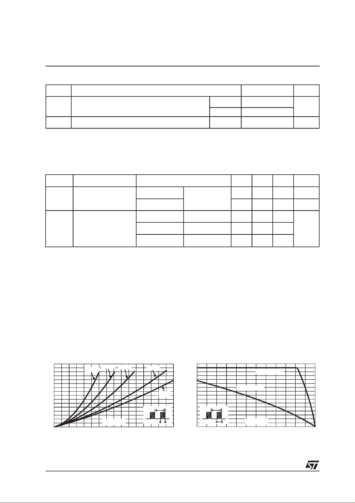
Fig. 1: Average forward power dissipation versus
averageforwardcurrent (per diode).
PF(av)(W)
16
14
12
10
8
6
4
2
0
0 2 4 6 8 10 12 14 16
δ= 0.05
δ = 0.1
IF(av) (A)
δ = 0.2
δ = 0.5
=tp/T
δ
δ =1
T
tp
R=VRRM
30 µA
525mA
=20A
F
=20A
F
=10A
F
0.58 0.65
0.96 V
0.8
Fig. 2: Average current versus ambient
temperature(δ = 0.5) (per diode).
IF(av)(A)
16
14
12
10
8
6
4
2
0
0 25 50 75 100 125 150
δ
T
=tp/T
Rth(j-a)=15°C/W
tp
Rth(j-a)=Rth(j-c)
Tamb(°C)
2/4

STPS3060CW
Fig. 3: Non repetitive surge peak forward
current versus overload duration (maximum
values) (per diode).
IM(A)
160
140
120
100
Tc=50°C
Tc=75°C
80
60
40
IM
20
0
1E-3 1E-2 1E-1 1E+0
δ=0.5
t
t(s)
Tc=110°C
Fig. 5: Reverse leakage current versus reverse
voltageapplied(typical values) (per diode).
IR(mA)
1E+1
1E+0
1E-1
1E-2
Tj=125°C
Tj=100°C
Tj=75°C
Tj=50°C
Fig. 4: Relative variation of thermal transient
impedancejunction to case versus pulseduration
(perdiode).
Zth(j-c)/Rth(j-c)
1.0
0.8
δ = 0.5
0.6
δ = 0.2
0.4
δ = 0.1
0.2
Single pulse
0.0
1E-3 1E-2 1E-1 1E+0
t(s)
δ
=tp/T
T
tp
Fig. 6: Junction capacitance versus reverse
voltageapplied(typicalvalues) (per diode).
C(pF)
1000
500
200
F=1MHz
Tj=25°C
1E-3
5 1015202530354045505560
VR(V)
Fig. 7: Forward voltage drop versus forward
current(maximum values)(per diode).
VFM(V)
1.8
Tj=125°C
1.6
1.4
1.2
1.0
0.8
0.6
0.4
0.2
0.0
0.1 1 10 100 200
IFM(A)
100
12 51020 60
VR(V)
3/4

STPS3060CW
PACKAGEMECHANICAL DATA
TO247
V
V
H
L5
L
F4
F3
F2
L1
L3
F1
V2
F(x3)
G
==
Dia.
L4L2
D
ME
A
DIMENSIONS
REF.
Millimeters Inches
Min. Typ. Max. Min. Typ. Max.
A 4.85 5.15 0.191 0.203
D 2.20 2.60 0.086 0.102
E 0.40 0.80 0.015 0.031
F 1.00 1.40 0.039 0.055
F1 3.00 0.118
F2 2.00 0.078
F3 2.00 2.40 0.078 0.094
F4 3.00 3.40 0.118 0.133
G 10.90 0.429
H 15.45 15.75 0.608 0.620
L 19.85 20.15 0.781 0.793
L1 3.70 4.30 0.145 0.169
L2 18.50 0.728
L3 14.20 14.80 0.559 0.582
L4 34.60 1.362
L5 5.50 0.216
M 2.00 3.00 0.078 0.118
V5° 5°
V2 60° 60°
Dia. 3.55 3.65 0.139 0.143
Marking:STPS3060CW
Coolingmethod : C
Weight: 4.4 g
Recommendedtorquevalue : 0.8m.N
Maximumtorque value :1.0m.N
Informationfurnished is believed tobe accurateand reliable. However, STMicroelectronics assumes no responsIbilityfor theconsequences of
use ofsuch information norfor any infringementof patentsor other rightsof third parties which mayresult from itsuse. No license isgranted by
implication or otherwise under any patent or patent rights of STMicroelectronics.Specifications mentioned in this publication are subject to
change withoutnotice. This publicationsupersedes andreplaces all information previously supplied.
STMicroelectronics products are not authorized for use as criticalcomponentsin life support devices or systems withoutexpress written approval ofSTMicroelectronics.
The ST logo is a registered trademark of STMicroelectronics
1998 STMicroelectronics - Printed in Italy - All rightsreserved.
STMicroelectronics GROUP OF COMPANIES
Australia - Brazil - Canada - China - France - Germany - Italy - Japan - Korea - Malaysia - Malta - Mexico - Morocco -
The Netherlands Singapore - Spain - Sweden - Switzerland - Taiwan - Thailand - United Kingdom - U.S.A.
4/4
 Loading...