

SGS Thomson Microelectronics ST93C56, ST93C56C, ST93C57C Datasheet
2K (128 x 16 or 256 x 8)SERIALMICROWIREEEPROM
1 MILLIONERASE/WRITE CYCLES, with
40 YEARS DATARETENTION
DUALORGANIZATION:128 x 16 or 256 x 8
BYTE/WORDand ENTIRE MEMORY
PROGRAMMINGINSTRUCTIONS
SELF-TIMED PROGRAMMINGCYCLE with
AUTO-ERASE
READY/BUSYSIGNALDURING
PROGRAMMING
SINGLESUPPLYVOLTAGE:
– 4.5V to 5.5V for ST93C56version
– 3V to 5.5V for ST93C57 version
SEQUENTIALREAD OPERATION
5ms TYPICALPROGRAMMINGTIME
ST93C56,ST93C56C,ST93C57Care
replacedby the M93C56
ST93C56, 56C
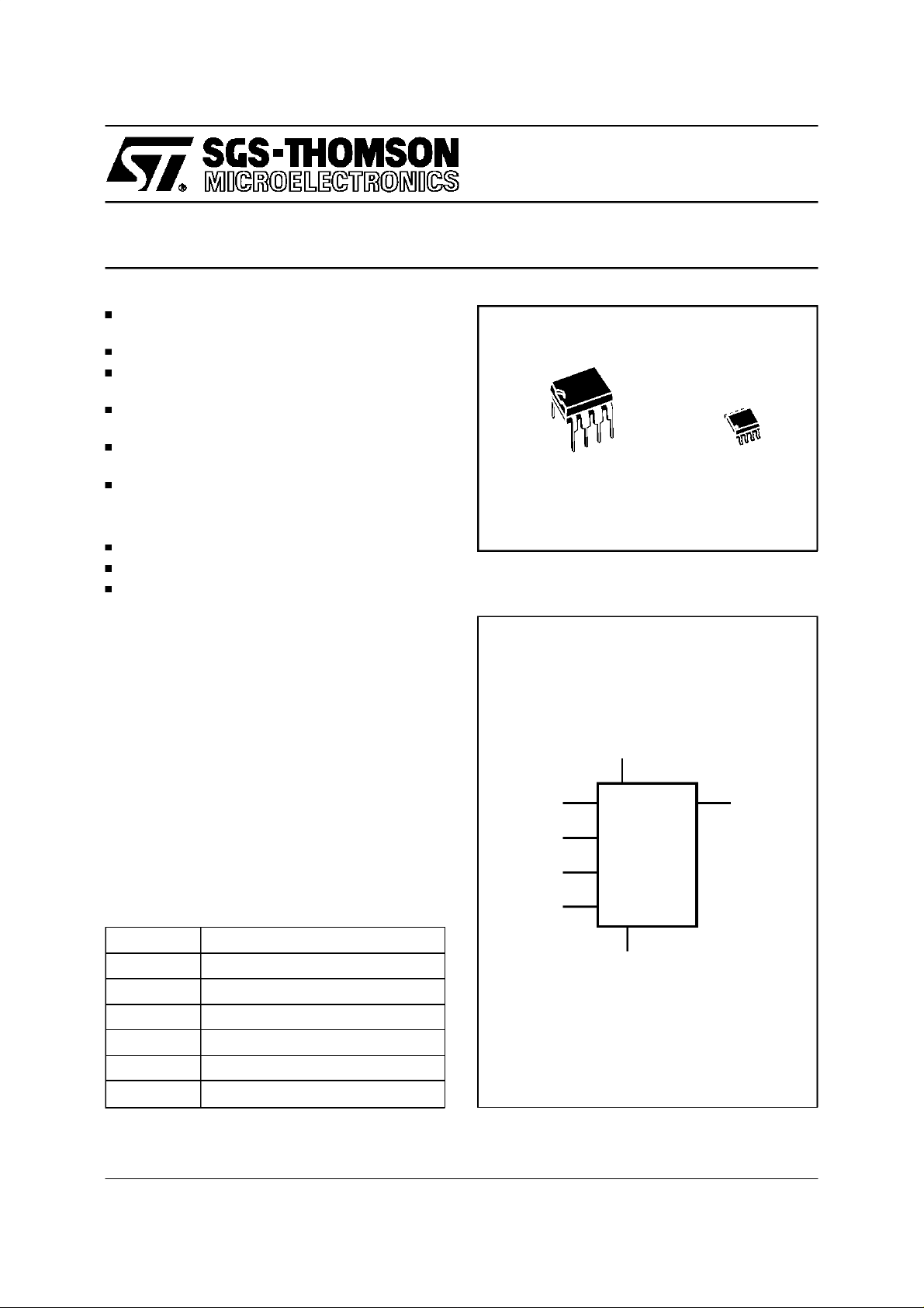
8
1
PSDIP8 (B)
0.4mm Frame
Figure 1. Logic Diagram
ST93C57C
NOT FOR NEW DESIGN
8
1
SO8 (M)
150mil Width
DESCRIPTION
This specification covers a range of 2K bit serial
EEPROM products, the ST93C56, 56C specified
at 5V ± 10%and the ST93C57C specified at 3Vto
5.5V. In the text, products are referred to as
ST93C56.
The ST93C56 is a 2K bit Electrically Erasable
ProgrammableMemory(EEPROM)fabricatedwith
SGS-THOMSON’sHighEnduranceSinglePolysilicon CMOS technology. The memory is accessed
through a serial input (D) and output (Q). The 2K
bit memory is divided into either 256 x 8 bit bytes
or 128 x 16 bit words. The organization may be
selectedby a signalappliedon the ORG input.
Table 1. Signal Names
S Chip Select Input
D Serial Data Input
Q Serial Data Output
C Serial Clock
ORG Organisation Select
V
CC
V
SS
Supply Voltage
Ground
ORG
V
CC
D
C
S
ST93C56
ST93C57
V
SS
Q
AI00881C
June 1997 1/13
This isinformation on a productstill in productionbutnot recommendedfor new designs.
ST93C56/56C, ST93C57C
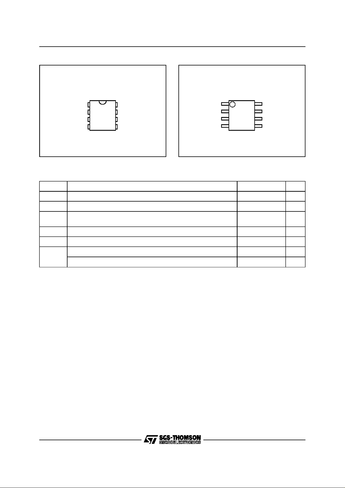
Figure2A. DIPPin Connections
ST93C56
ST93C57
SV
1
2
D
3
Q
4
Warning: DU = Don’t Use Warning: DU = Don’t Use
Table 2. Absolute MaximumRatings
Symbol Parameter Value Unit
T
T
T
STG
LEAD
Ambient Operating Temperature –40 to125 °C
A
Storage Temperature –65 to150 °C
Lead Temperature,Soldering (SO8 package)
8
7
6
5
AI00882C
CC
DUC
ORG
V
SS
(1)
(PSDIP8 package)
Figure2B. SO Pin Connections
ST93C56
ST93C57
1
SV
2
D
3
Q
4
40 sec
10 sec
8
7
6
5
AI00883D
215
260
CC
DUC
ORG
V
SS
°C
V
V
CC
V
ESD
Notes: 1. Exceptfor the rating ”Operating Temperature Range”, stresses above those listed in the Table ”Absolute Maximum Ratings”
DESCRIPTION (cont’d)
Input or Output Voltages(Q = VOHor Hi-Z) –0.3 to VCC+0.5 V
IO
Supply Voltage –0.3 to 6.5 V
Electrostatic Discharge Voltage (Human Body model)
Electrostatic Discharge Voltage (Machine model)
may cause permanent damage to thedevice. These are stress ratings only and operation of the device at these or any other
conditions abovethose indicated in the Operating sections of this specification is not implied. Exposure toAbsolute Maximum
Rating conditions for extended periods may affect device reliability.Refer also to the SGS-THOMSON SURE Program and other
relevant quality documents.
2. MIL-STD-883C, 3015.7(100pF, 1500 Ω).
3. EIAJ IC-121 (Condition C) (200pF, 0 Ω).
(2)
(3)
4000 V
500 V
nectedorleftrunningafterthestart ofa Writecycle)
and does not require an erase cycle prior to the
The memory is accessed by a set of instructions
which includes Read a byte/word, Write a
byte/word,Erasea byte/word, Erase All and Write
All. AReadinstructionloads theaddressof the first
byte/word to be read into an internal address
pointer. The datacontained at this addressis then
clocked out serially. The address pointer is automaticallyincrementedafter the data is output and,
if the Chip Select input (S) is held High, the
ST93C56 can output a sequential stream of data
bytes/words.In this way,the memorycan be read
as a data stream from 8 to 2048 bits long, or
continuouslyas the addresscounterautomatically
rolls over to ’00’ when the highest address is
reached.Programming is internally self-timed (the
external clock signal on C input may be discon-
Write instruction. The Write instruction writes8 or
16 bits at one time into oneof the256bytesor128
words. After the startof the programming cycle, a
Busy/Readysignal is available on the Data output
(Q)when Chip Select (S) is driven High.
The design of the ST93C56 and the High Endur-
anceCMOStechnologyusedforitsfabricationgive
an Erase/Write cycle Enduranceof 1,000,000cy-
clesand a data retention of 40 years.
TheDU (Don’tUse) pindoes notaffectthefunction
of the memory and it is reserved for use by SGS-
THOMSON duringtestsequences.Thepinmaybe
left unconnectedor may be connected to V
V
. Direct connection of DU to VSSis recom-
SS
mended for the lowest standby power consump-
tion.
CC
or
2/13
ST93C56/56C, ST93C57C
AC MEASUREMENT CONDITIONS
Figure 3. ACTesting Input Output Waveforms
Input Rise and Fall Times ≤ 20ns
Input Pulse Voltages 0.4V to 2.4V
Input Timing Reference Voltages 1V to 2.0V
Output Timing Reference Voltages 0.8V to 2.0V
Note that Output Hi-Z is defined as the point where data
2.4V
0.4V
2V
1V
INPUT OUTPUT
is no longer driven.
Table 3. Capacitance
(1)
(TA=25°C, f =1 MHz )
Symbol Parameter Test Condition Min Max Unit
C
IN
C
OUT
Note: 1. Sampled only, not 100% tested.
Input Capacitance VIN=0V 5 pF
Output Capacitance V
=0V 5 pF
OUT
Table 4. DC Characteristics
= 0 to70°C or –40 to 85°C; VCC= 4.5V to 5.5V or 3V to 5.5V)
(T
A
Symbol Parameter TestCondition Min Max Unit
I
I
I
CC1
V
V
V
V
I
LI
LO
CC
IL
IH
OL
OH
Input Leakage Current 0V ≤ VIN≤ V
Output Leakage Current
0V ≤ V
≤ VCC,
OUT
Q inHi-Z
CC
±2.5 µA
±2.5 µA
Supply Current (TTL Inputs) S = VIH, f = 1 MHz 3 mA
Supply Current (CMOS Inputs) S = V
Supply Current (Standby)
Input Low Voltage (D, C, S)
Input High Voltage (D, C, S)
Output Low Voltage
Output High Voltage
, f = 1 MHz 2 mA
IH
,C=VSS,
S=V
SS
ORG = V
V
CC
3V ≤ V
V
CC
3V ≤ V
I
OL
I
I
OH
I
OH
or V
SS
CC
=5V±10% –0.3 0.8 V
≤ 4.5V –0.3 0.2V
CC
=5V±10% 2 VCC+1 V
≤ 4.5V 0.8 V
CC
CC
= 2.1mA 0.4 V
=10µA 0.2 V
OL
= –400µA 2.4 V
= –10µAV
–0.2 V
CC
50 µA
VCC+1 V
CC
2.0V
0.8V
AI00815
V
3/13
ST93C56/56C, ST93C57C
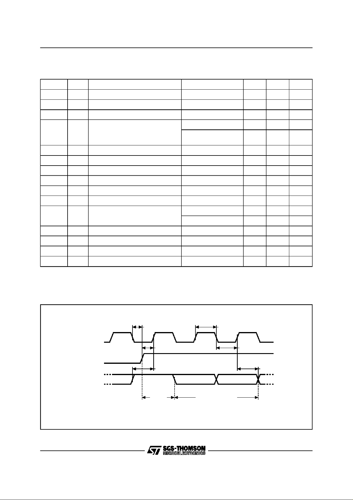
Table 5. AC Characteristics
(T
= 0 to70°C or –40 to 85°C; VCC= 4.5V to 5.5V or 3V to 5.5V)
A
Symbol Alt Parameter Test Condition Min Max Unit
t
SHCH
t
CLSH
t
DVCH
t
CHDX
t
t
t
t
Chip Select High to Clock High 50 ns
CSS
Clock Low to Chip Select High 100 ns
SKS
Input Valid to Clock High 100 ns
DIS
Temp.Range: grade 1 100 ns
Clock High to Input Transition
DIH
Temp.Range:
grades 3, 6
200 ns
t
CHQL
t
CHQV
t
CLSL
t
SLCH
t
SLSH
t
SHQV
t
SLQZ
t
PD0
t
PD1
t
CSH
t
t
t
Clock High to Output Low 500 ns
Clock High to Output Valid 500 ns
Clock Low to Chip Select Low 0 ns
Chip Select Low to ClockHigh 250 ns
Chip Select Low to Chip Select High Note 1 250 ns
CS
Chip Select High to Output Valid 500 ns
SV
Chip Select Low to Output Hi-Z
DF
ST93C56 300 ns
ST93C56C, 57C 200 ns
t
CHCL
t
CLCH
t
W
f
C
Notes: 1. Chip Select must bebrought low for a minimum of 250 ns(t
2. The Clock frequency specification calls for aminimum clock period of 1 µs, therefore the sum of the timings t
t
t
must be greater or equal to 1 µs. For example, ift
Clock High to Clock Low Note 2 250 ns
SKH
Clock Low to Clock High Note 2 250 ns
SKL
t
Erase/Write Cycle time 10 ms
WP
f
Clock Frequency 0 1 MHz
SK
) betweenconsecutive instructioncycles.
SLSH
is 250 ns, then t
CHCL
must be at least 750ns.
CLCH
Figure4. Synchronous Timing, Start and Op-CodeInput
CHCL+tCLCH
4/13
tCLSH tCHCL
C
tSHCH
S
tDVCH
D
OP CODE OP CODESTART
OP CODE INPUTSTART
tCLCH
tCHDX
AI01428
 Loading...