

SGS Thomson Microelectronics ST93C47T, ST93C47C, ST93C46T, ST93C46C, ST93C46A Datasheet
1K (64 x 16 or 128 x 8) SERIAL MICROWIREEEPROM
1 MILLIONERASE/WRITE CYCLES, with
40 YEARS DATARETENTION
DUALORGANIZATION:64 x 16 or 128 x 8
BYTE/WORDand ENTIRE MEMORY
PROGRAMMINGINSTRUCTIONS
SELF-TIMED PROGRAMMINGCYCLE with
AUTO-ERASE
READY/BUSYSIGNALDURING
PROGRAMMING
SINGLESUPPLYVOLTAGE:
– 4.5V to 5.5V for ST93C46version
– 3V to 5.5V forST93C47 version
SEQUENTIALREAD OPERATION
5ms TYPICALPROGRAMMING TIME
ENHANCED ESD/LATCH UP
PERFORMANCEfor ”C” VERSION
ST93C46A,ST93C46C, ST93C46T,
ST93C47C,ST93C47T are replacedby the
M93C46
ST93C46A,46C,46T
ST93C47C,47T
8
1
PSDIP8 (B)
0.4mm Frame
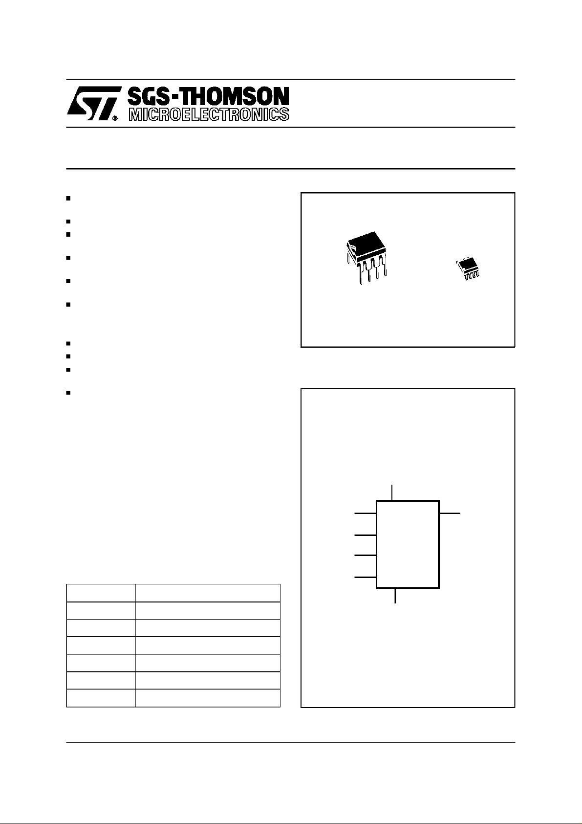
Figure 1. Logic Diagram
NOT FOR NEW DESIGN
8
1
SO8 (M)
150mil Width
DESCRIPTION
This specification covers a range of 1K bit serial
EEPROM products, the ST93C46A,46C,46T
specified at 5V±10% and the ST93C47C,47T
specifiedat 3V to 5.5V.
In the text, products are referred to as ST93C46.
The ST93C46 is a 1K bit Electrically Erasable
ProgrammableMemory(EEPROM)fabricatedwith
SGS-THOMSON’sHighEnduranceSinglePolysilicon CMOS technology. The memory is accessed
througha serial input (D) and output(Q).
Table 1. Signal Names
S Chip Select Input
D Serial Data Input
Q Serial Data Output
C Serial Clock
ORG Organisation Select
V
CC
V
SS
Supply Voltage
Ground
ORG
V
CC
D
C
S
ST93C46
ST93C47
V
SS
Q
AI00871C
June 1997 1/13
This isinformation on a productstill in productionbutnot recommendedfor new designs.

ST93C46A/46C/46T, ST93C47C/47T
Table 2. Absolute Maximum Ratings
Symbol Parameter Value Unit
T
T
STG
T
LEAD
V
V
CC
V
ESD
Notes: 1. Exceptfor the rating ”Operating Temperature Range”, stresses above those listed in the Table”Absolute Maximum Ratings”
Ambient Operating Temperature –40 to 125 °C
A
Storage Temperature –65 to150 °C
Lead Temperature,Soldering (SO8 package)
Input or Output Voltages(Q = VOHor Hi-Z) –0.3 to VCC+0.5 V
IO
Supply Voltage –0.3 to 6.5 V
Electrostatic Discharge Voltage (Human Body model)
Electrostatic Discharge Voltage (Machine model)
may cause permanent damage to the device. These are stress ratings only and operationof the device at these or any other
conditions abovethose indicated in the Operating sections of this specification is not implied. Exposure toAbsolute Maximum
Rating conditions for extended periods may affect device reliability.Refer also to the SGS-THOMSON SURE Program and other
relevant quality documents.
2. MIL-STD-883C, 3015.7(100pF, 1500 Ω).
3. EIAJ IC-121 (Condition C) (200pF, 0 Ω).
Figure2A. DIP Pin Connections
(1)
(PSDIP8 package)
40 sec
10 sec
(2)
ST93C46A,T
ST93C46C
(3)
ST93C46 500 V
215
260
2000
4000
Figure2B. SO Pin Connections
°C
V
ST93C46
ST93C47
SV
1
2
D
3
Q
4
Warning: DU = Don’t Use
8
7
6
5
AI00872C
CC
DUC
ORG
V
SS
Figure2C. SO, 90° Turn, Pin Connections
ST93C46T
ST93C47T
DU ORG
V
CC
Warning: DU = Don’t Use
1
2
S
3
4
AI00982B
8
V
7
SS
Q
6
DC
5
ST93C46
ST93C47
1
SV
2
D
3
Q
4
Warning: DU = Don’t Use
8
7
6
5
AI00874C
CC
DUC
ORG
V
SS
DESCRIPTION (cont’d)
The1K bitmemoryis dividedinto either 128 x 8 bit
bytes or 64 x 16 bit words. The organizationmay
be selected by a signal on the ORG input. The
memoryis accessedby a set of instructionswhich
includes Read a byte/word, Write a byte/word,
Erasea byte/word, EraseAll andWrite All.
A Read instruction loads the address of the first
byte/word to be read into an internal address
pointer.The data is then clocked out serially.
The address pointer is automatically incremented
afterthe data isoutputand,if theChipSelectinput
(S)isheldHigh, theST93C46canoutputa sequential stream of data bytes/words. In this way, the
memory can be read as a data stream from 8 to
1024 bits long, or continuously as the address
2/13

ST93C46A/46C/46T, ST93C47C/47T
AC MEASUREMENT CONDITIONS
Figure 3. ACTesting Input Output Waveforms
Input Rise and Fall Times ≤ 20ns
Input Pulse Voltages 0.4V to 2.4V
2.4V
2V
Input Timing Reference Voltages 1V to 2.0V
Output Timing Reference Voltages 0.8V to 2.0V
0.4V
1V
INPUT OUTPUT
Note that Output Hi-Z is defined as the point where data
is no longer driven.
Table 3. Capacitance
(1)
(TA=25°C, f = 1 MHz)
Symbol Parameter Test Condition Min Max Unit
C
IN
C
OUT
Note: 1. Sampled only, not 100% tested.
Input Capacitance VIN=0V 5 pF
Output Capacitance V
=0V 5 pF
OUT
Table 4. DC Characteristics
(T
= 0 to70°C or –40 to 85°C; VCC= 4.5V to 5.5V or 3V to 5.5V)
A
Symbol Parameter TestCondition Min Max Unit
I
I
I
CC1
V
V
V
V
I
LI
LO
CC
IL
IH
OL
OH
Input Leakage Current 0V ≤ VIN≤ V
Output Leakage Current
0V ≤ V
≤ VCC,
OUT
Q inHi-Z
CC
±2.5 µA
±2.5 µA
Supply Current (TTL Inputs) S = VIH, f = 1 MHz 3 mA
Supply Current (CMOS Inputs) S = V
Supply Current (Standby)
Input Low Voltage (D, C, S)
Input High Voltage (D, C, S)
Output Low Voltage
Output High Voltage
, f = 1 MHz 2 mA
IH
,C=VSS,
S=V
SS
ORG = V
V
CC
3V ≤ V
V
CC
3V ≤ V
I
OL
I
I
OH
I
OH
or V
SS
CC
=5V±10% –0.3 0.8 V
≤ 4.5V –0.3 0.2V
CC
=5V±10% 2 VCC+1 V
≤ 4.5V 0.8 V
CC
CC
= 2.1mA 0.4 V
=10µA 0.2 V
OL
= –400µA 2.4 V
= –10µAV
–0.2 V
CC
50 µA
VCC+1 V
CC
2.0V
0.8V
AI00815
V
3/13

ST93C46A/46C/46T, ST93C47C/47T
Table 5. AC Characteristics
(T
= 0 to70°C or –40 to 85°C; VCC= 4.5V to 5.5V or 3V to 5.5V)
A
Symbol Alt Parameter Test Condition Min Max Unit
t
SHCH
t
CLSH
t
DVCH
t
CHDX
t
CSS
t
SKS
t
t
Chip Select High to Clock High 50 ns
Clock Low to Chip Select High 100 ns
Input Valid to Clock High 100 ns
DIS
Temp.Range: grade 1 100 ns
Clock High to Input Transition
DIH
Temp.Range:
grades 3, 6
200 ns
t
CHQL
t
CHQV
t
CLSL
t
SLCH
t
SLSH
t
SHQV
t
SLQZ
t
PD0
t
PD1
t
CSH
t
t
t
Clock High to Output Low 500 ns
Clock High to Output Valid 500 ns
Clock Low to Chip Select Low 0 ns
Chip Select Low to ClockHigh 250 ns
Chip Select Low to Chip Select High Note 1 250 ns
CS
Chip Select High to Output Valid 500 ns
SV
Chip Select Low to Output Hi-Z
DF
ST93C46A 300 ns
ST93C46C, 47C 200 ns
t
CHCL
t
CLCH
t
W
f
C
Notes: 1. Chip Select must bebrought low for a minimum of 250 ns(t
2. The Clock frequency specification calls for aminimum clock period of 1 µs, therefore the sum of the timings t
t
t
must be greater or equal to 1 µs. For example, ift
Clock High to Clock Low Note 2 250 ns
SKH
Clock Low to Clock High Note 2 250 ns
SKL
t
Erase/Write Cycle time 10 ms
WP
f
Clock Frequency 0 1 MHz
SK
) betweenconsecutive instructioncycles.
SLSH
is 250 ns, then t
CHCL
must be at least 750ns.
CLCH
Figure4. SynchronousTiming,Start and Op-Code Input
CHCL+tCLCH
4/13
tCLSH tCHCL
C
tSHCH
S
tDVCH
D
OP CODE OP CODESTART
OP CODE INPUTSTART
tCLCH
tCHDX
AI01428
 Loading...