

Datasheet ST93C47T, ST93C47C, ST93C46T, ST93C46C, ST93C46A Datasheet (SGS Thomson Microelectronics)
Page 1
1K (64 x 16 or 128 x 8) SERIAL MICROWIREEEPROM
1 MILLIONERASE/WRITE CYCLES, with
40 YEARS DATARETENTION
DUALORGANIZATION:64 x 16 or 128 x 8
BYTE/WORDand ENTIRE MEMORY
PROGRAMMINGINSTRUCTIONS
SELF-TIMED PROGRAMMINGCYCLE with
AUTO-ERASE
READY/BUSYSIGNALDURING
PROGRAMMING
SINGLESUPPLYVOLTAGE:
– 4.5V to 5.5V for ST93C46version
– 3V to 5.5V forST93C47 version
SEQUENTIALREAD OPERATION
5ms TYPICALPROGRAMMING TIME
ENHANCED ESD/LATCH UP
PERFORMANCEfor ”C” VERSION
ST93C46A,ST93C46C, ST93C46T,
ST93C47C,ST93C47T are replacedby the
M93C46
ST93C46A,46C,46T
ST93C47C,47T
8
1
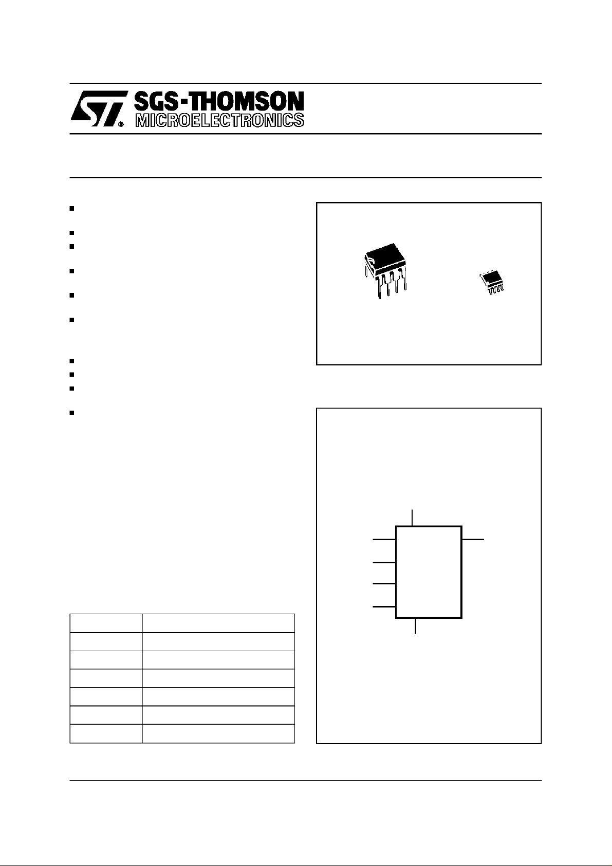
PSDIP8 (B)
0.4mm Frame
Figure 1. Logic Diagram
NOT FOR NEW DESIGN
8
1
SO8 (M)
150mil Width
DESCRIPTION
This specification covers a range of 1K bit serial
EEPROM products, the ST93C46A,46C,46T
specified at 5V±10% and the ST93C47C,47T
specifiedat 3V to 5.5V.
In the text, products are referred to as ST93C46.
The ST93C46 is a 1K bit Electrically Erasable
ProgrammableMemory(EEPROM)fabricatedwith
SGS-THOMSON’sHighEnduranceSinglePolysilicon CMOS technology. The memory is accessed
througha serial input (D) and output(Q).
Table 1. Signal Names
S Chip Select Input
D Serial Data Input
Q Serial Data Output
C Serial Clock
ORG Organisation Select
V
CC
V
SS
Supply Voltage
Ground
ORG
V
CC
D
C
S
ST93C46
ST93C47
V
SS
Q
AI00871C
June 1997 1/13
This isinformation on a productstill in productionbutnot recommendedfor new designs.
Page 2

ST93C46A/46C/46T, ST93C47C/47T
Table 2. Absolute Maximum Ratings
Symbol Parameter Value Unit
T
T
STG
T
LEAD
V
V
CC
V
ESD
Notes: 1. Exceptfor the rating ”Operating Temperature Range”, stresses above those listed in the Table”Absolute Maximum Ratings”
Ambient Operating Temperature –40 to 125 °C
A
Storage Temperature –65 to150 °C
Lead Temperature,Soldering (SO8 package)
Input or Output Voltages(Q = VOHor Hi-Z) –0.3 to VCC+0.5 V
IO
Supply Voltage –0.3 to 6.5 V
Electrostatic Discharge Voltage (Human Body model)
Electrostatic Discharge Voltage (Machine model)
may cause permanent damage to the device. These are stress ratings only and operationof the device at these or any other
conditions abovethose indicated in the Operating sections of this specification is not implied. Exposure toAbsolute Maximum
Rating conditions for extended periods may affect device reliability.Refer also to the SGS-THOMSON SURE Program and other
relevant quality documents.
2. MIL-STD-883C, 3015.7(100pF, 1500 Ω).
3. EIAJ IC-121 (Condition C) (200pF, 0 Ω).
Figure2A. DIP Pin Connections
(1)
(PSDIP8 package)
40 sec
10 sec
(2)
ST93C46A,T
ST93C46C
(3)
ST93C46 500 V
215
260
2000
4000
Figure2B. SO Pin Connections
°C
V
ST93C46
ST93C47
SV
1
2
D
3
Q
4
Warning: DU = Don’t Use
8
7
6
5
AI00872C
CC
DUC
ORG
V
SS
Figure2C. SO, 90° Turn, Pin Connections
ST93C46T
ST93C47T
DU ORG
V
CC
Warning: DU = Don’t Use
1
2
S
3
4
AI00982B
8
V
7
SS
Q
6
DC
5
ST93C46
ST93C47
1
SV
2
D
3
Q
4
Warning: DU = Don’t Use
8
7
6
5
AI00874C
CC
DUC
ORG
V
SS
DESCRIPTION (cont’d)
The1K bitmemoryis dividedinto either 128 x 8 bit
bytes or 64 x 16 bit words. The organizationmay
be selected by a signal on the ORG input. The
memoryis accessedby a set of instructionswhich
includes Read a byte/word, Write a byte/word,
Erasea byte/word, EraseAll andWrite All.
A Read instruction loads the address of the first
byte/word to be read into an internal address
pointer.The data is then clocked out serially.
The address pointer is automatically incremented
afterthe data isoutputand,if theChipSelectinput
(S)isheldHigh, theST93C46canoutputa sequential stream of data bytes/words. In this way, the
memory can be read as a data stream from 8 to
1024 bits long, or continuously as the address
2/13
Page 3

ST93C46A/46C/46T, ST93C47C/47T
AC MEASUREMENT CONDITIONS
Figure 3. ACTesting Input Output Waveforms
Input Rise and Fall Times ≤ 20ns
Input Pulse Voltages 0.4V to 2.4V
2.4V
2V
Input Timing Reference Voltages 1V to 2.0V
Output Timing Reference Voltages 0.8V to 2.0V
0.4V
1V
INPUT OUTPUT
Note that Output Hi-Z is defined as the point where data
is no longer driven.
Table 3. Capacitance
(1)
(TA=25°C, f = 1 MHz)
Symbol Parameter Test Condition Min Max Unit
C
IN
C
OUT
Note: 1. Sampled only, not 100% tested.
Input Capacitance VIN=0V 5 pF
Output Capacitance V
=0V 5 pF
OUT
Table 4. DC Characteristics
(T
= 0 to70°C or –40 to 85°C; VCC= 4.5V to 5.5V or 3V to 5.5V)
A
Symbol Parameter TestCondition Min Max Unit
I
I
I
CC1
V
V
V
V
I
LI
LO
CC
IL
IH
OL
OH
Input Leakage Current 0V ≤ VIN≤ V
Output Leakage Current
0V ≤ V
≤ VCC,
OUT
Q inHi-Z
CC
±2.5 µA
±2.5 µA
Supply Current (TTL Inputs) S = VIH, f = 1 MHz 3 mA
Supply Current (CMOS Inputs) S = V
Supply Current (Standby)
Input Low Voltage (D, C, S)
Input High Voltage (D, C, S)
Output Low Voltage
Output High Voltage
, f = 1 MHz 2 mA
IH
,C=VSS,
S=V
SS
ORG = V
V
CC
3V ≤ V
V
CC
3V ≤ V
I
OL
I
I
OH
I
OH
or V
SS
CC
=5V±10% –0.3 0.8 V
≤ 4.5V –0.3 0.2V
CC
=5V±10% 2 VCC+1 V
≤ 4.5V 0.8 V
CC
CC
= 2.1mA 0.4 V
=10µA 0.2 V
OL
= –400µA 2.4 V
= –10µAV
–0.2 V
CC
50 µA
VCC+1 V
CC
2.0V
0.8V
AI00815
V
3/13
Page 4

ST93C46A/46C/46T, ST93C47C/47T
Table 5. AC Characteristics
(T
= 0 to70°C or –40 to 85°C; VCC= 4.5V to 5.5V or 3V to 5.5V)
A
Symbol Alt Parameter Test Condition Min Max Unit
t
SHCH
t
CLSH
t
DVCH
t
CHDX
t
CSS
t
SKS
t
t
Chip Select High to Clock High 50 ns
Clock Low to Chip Select High 100 ns
Input Valid to Clock High 100 ns
DIS
Temp.Range: grade 1 100 ns
Clock High to Input Transition
DIH
Temp.Range:
grades 3, 6
200 ns
t
CHQL
t
CHQV
t
CLSL
t
SLCH
t
SLSH
t
SHQV
t
SLQZ
t
PD0
t
PD1
t
CSH
t
t
t
Clock High to Output Low 500 ns
Clock High to Output Valid 500 ns
Clock Low to Chip Select Low 0 ns
Chip Select Low to ClockHigh 250 ns
Chip Select Low to Chip Select High Note 1 250 ns
CS
Chip Select High to Output Valid 500 ns
SV
Chip Select Low to Output Hi-Z
DF
ST93C46A 300 ns
ST93C46C, 47C 200 ns
t
CHCL
t
CLCH
t
W
f
C
Notes: 1. Chip Select must bebrought low for a minimum of 250 ns(t
2. The Clock frequency specification calls for aminimum clock period of 1 µs, therefore the sum of the timings t
t
t
must be greater or equal to 1 µs. For example, ift
Clock High to Clock Low Note 2 250 ns
SKH
Clock Low to Clock High Note 2 250 ns
SKL
t
Erase/Write Cycle time 10 ms
WP
f
Clock Frequency 0 1 MHz
SK
) betweenconsecutive instructioncycles.
SLSH
is 250 ns, then t
CHCL
must be at least 750ns.
CLCH
Figure4. SynchronousTiming,Start and Op-Code Input
CHCL+tCLCH
4/13
tCLSH tCHCL
C
tSHCH
S
tDVCH
D
OP CODE OP CODESTART
OP CODE INPUTSTART
tCLCH
tCHDX
AI01428
Page 5

Figure5. SynchronousTiming,Read or Write
C
S
ST93C46A/46C/46T, ST93C47C/47T
tCLSL
tDVCH
D
Q
C
S
D
Q
Hi-Z
An
tCHQL
ADDRESS INPUT
tDVCH
An
Hi-Z
A0
A0/D0
tCHQVtCHDX
tSLQZ
Q15/Q7 Q0
DATA OUTPUT
tSLCH
tCLSL
tSLSHtCHDX
BUSY
tSLQZ
READY
tSHQV
tW
tSLSH
AI00820C
ADDRESS/DATA INPUT
DESCRIPTION (cont’d)
counter automatically rolls over to ’00’ when the
highest addressis reached.
Programmingis internally self-timed (the external
clocksignalon C input may be disconnectedor left
running after the start of a Write cycle) and does
notrequirean erasecyclepriortotheWriteinstruction. The Writeinstructionwrites 8or 16 bitsat one
time into one of the 128 bytes or 64 words. After
the start of the programming cycle a Busy/Ready
signal is available on the Data output (Q) when
Chip Select (S) is High.
WRITE CYCLE
AI01429
An internal feature of the ST93C46 provides
Power-on Data Protection by inhibiting any operation when the Supply is toolow. Thedesign of the
ST93C46and theHigh EnduranceCMOStechnology used for its fabrication give an Erase/Write
cycle Endurance of 1,000,000 cycles and a data
retentionof 40 years.
The DU(Don’tUse) pindoesnotaffectthefunction
of the memory and it is reserved for use by SGSTHOMSONduringtestsequences.The pinmaybe
left unconnected or may be connected to V
. Direct connection of DU to VSSis recom-
V
SS
CC
or
mended for the lowest standby power consumption.
5/13
Page 6

ST93C46A/46C/46T, ST93C47C/47T
MEMORY ORGANIZATION
The ST93C46 is organised as 128bytes x8 bitsor
64 words x 16 bits. If the ORG input is left unconnected(or connected to V
) the x16 organization
CC
is selected, when ORG is connected to Ground
) the x8 organization is selected. When the
(V
SS
ST93C46 is in standby mode, the ORG input
should be unconnectedor set to eitherV
SS
or V
CC
in order to get minimum power consumption. Any
voltagebetweenV
andVCCappliedto ORG may
SS
increase the standby current value.
POWER-ON DATA PROTECTION
During power-up, A Power On Reset sequenceis
run in order to reset all internal programming circuitry and the device is set in the Write Disable
mode. When V
reaches its functionalvalue, the
CC
deviceisproperlyreset (inthe Write Disablemode)
and is ready to decode and execute an incoming
instruction.
INSTRUCTIONS
The ST93C46 has seveninstructions,asshownin
Table 6. Each instruction is precededby the rising
edgeof thesignalapplied ontheS input (assuming
that theclock C is low), followedby a ’1’ read on D
input during the rising edge of the clock C. The
op-codes of the instructionsare made up of the 2
followingbits.Someinstructionsuseonlythesefirst
two bits, others use also the first two bits of the
address to define the op-code. The op-code is
followed by an addressfor the byte/wordwhich is
made up of six bits for the x16 organization or
sevenbits for the x8 organization.
The ST93C46 is fabricated in CMOS technology
and is therefore able to run from zero Hz (static
inputsignals)up to the maximumratings(specified
in Table 5).
Read
The Read instruction (READ) outputs serial data
on the Data Output (Q). Whena READ instruction
is received, the instruction and address are decodedandthedata fromthememoryistransferred
intoanoutputshiftregister.Adummy’0’bitisoutput
firstfollowedby the 8bitbyte orthe 16bit wordwith
the MSB first. Output data changes are triggered
by the Low to Hightransitionof the Clock (C). The
ST93C46will automaticallyincrement the address
and will clock outthe next byte/wordaslong as the
Chip Select input(S) is heldHigh. In this case the
dummy’0’ bit is NOToutput between bytes/words
and a continuousstream of data can be read.
Erase/WriteEnable and Disable
The Erase/Write Enable instruction (EWEN)
authorizesthefollowingErase/Writeinstructionsto
be executed, the Erase/Write Disable instruction
(EWDS) freezes the execution of the following
Erase/Write instructions. When power is first applied to the ST93C46, Erase/Write is inhibited.
When the EWEN instruction is executed, Write
instructions remain enabled until an Erase/Write
Disableinstruction(EWDS)is executedorV
CC
falls
belowthe power-on reset threshold.Toprotect the
memory contents from accidental corruption, it is
advisabletoissuetheEWDSinstructionafterevery
writecycle.
TheREADinstructionisnot affectedby the EWEN
or EWDS instructions.
Table 6. InstructionSet
Instruction Description Op-Code
READ Read Data from Memory 10 A6-A0 Q7-Q0 A5-A0 Q15-Q0
WRITE WriteData to Memory 01 A6-A0 D7-D0 A5-A0 D15-D0
EWEN Erase/Write Enable 00 11XXXXX 11XXXX
EWDS Erase/Write Disable 00 00XXXXX 00XXXX
ERASE Erase Byte or Word 11 A6-A0 A5-A0
ERAL Erase All Memory 00 10XXXXX 10XXXX
WRAL Write All Memorywith same Data 00 01XXXXX D7-D0 01XXXX D15-D0
Note: X = don’t care bit.
6/13
x8 Org
Address
(ORG = 0)
Data
x16 Org
Address
(ORG = 1)
Data
Page 7

ST93C46A/46C/46T, ST93C47C/47T
Erase
The Erase instruction (ERASE) programs the addressed memory byte or word bitsto ’1’. Oncethe
addressiscorrectlydecoded,thefallingedge ofthe
Chip Select input (S) starts a self-timed programming cycle.
If the ST93C46 is still performing the write cycle,
the Busysignal (Q= 0)willbereturnedif S isdriven
high, and the ST93C46will ignoreany dataon the
bus. When the write cycle iscompleted,the Ready
Figure6. READ, WRITE, EWEN,EWDS Sequences
READ
S
D
Q
110An A0
Qn Q0
ADDR
OP
CODE
signal (Q = 1) will indicate (if S is drivenhigh) that
the ST93C46is ready to receive a new instruction.
Write
The Write instruction (WRITE) is followed by the
addressandthe8or16 databitstobewritten.Data
input is sampled on the Low to High transition of
the clock.After thelast data bit hasbeensampled,
Chip Select (S) must be brought Low before the
next rising edge of the clock(C), in order to start
the self-timedprogramming cycle. If the ST93C46
is still performing the write cycle, the Busy signal
DATA OUT
SWRITE
D
Q
ERASE
WRITE
ENABLE
Notes: 1. An: n = 5 for x16 org.and 6 for x8 org.
2. Xn: n = 3 for x16 org. and 4 for x8 org.
S
1 0 An A0
OP
CODE
1 0 Xn X0D
OP
CODE
ADDR
101
CHECK
STATUS
Dn D01
DATA IN
ERASE
WRITE
DISABLE
S
BUSY READY
1 0 Xn X0D
000
OP
CODE
AI00878C
7/13
Page 8

ST93C46A/46C/46T, ST93C47C/47T
INSTRUCTIONS (cont’d)
(Q = 0) will be returned if Sis driven high, and the
ST93C46willignoreanydataon thebus.Whenthe
writecycle is completed, the Ready signal(Q = 1)
will indicate(if S is drivenhigh) that the ST93C46
is ready to receivea new instruction.
The Write instruction includesan automaticErase
cycle before writing the data, it is thereforeunnecessary to execute an Erase instruction before a
Writeinstruction execution.
Erase All
The Erase All instruction(ERAL) erasesthe whole
memory(all memorybits are set to ”1”). A dummy
addressis input duringthe instructiontransfer and
the erase is made in the sameway as the ERASE
instructionabove.IftheST93C46isstill performing
the write cycle, the Busy signal (Q = 0) will be
returnedif S is driven high, and the ST93C46will
Figure7. ERASE, ERAL Sequences
SERASE
11D
An A0
1
ignore any data on the bus. When the write cycle
is completed,the Readysignal (Q = 1)will indicate
(if S is driven high) that the ST93C46 is ready to
receive a new instruction.
Write All
For correct operation,an ERAL instructionshould
be executedbefore the WRALinstruction.
The Write All instruction (WRAL) writes the Data
Input byte or word to all the addresses of the
memory. In the WRAL instruction, NO automatic
erase is made so all bytes/words must be erased
beforetheWRALinstruction. If the ST93C46is still
performing the write cycle, the Busy signal (Q = 0)
willbereturnedif Sisdrivenhigh,and theST93C46
will ignore any data on the bus. When the write
cycle is completed, the Ready signal (Q = 1) will
indicate (if S is driven high) that the ST93C46 is
ready to receive a newinstruction.
CHECK
STATUS
Q
ERASE
ALL
Notes: 1. An: n = 5 for x16 org.and 6 for x8 org.
2. Xn: n = 3 for x16 org. and 4 for x8 org.
8/13
S
Q
OP
CODE
10D
00
1
OP
CODE
ADDR
Xn X0
ADDR
BUSY READY
CHECK
STATUS
BUSY READY
AI00879B
Page 9

Figure8. WRAL Sequence
ST93C46A/46C/46T, ST93C47C/47T
ALL
Note: 1. Xn: n = 3 for x16 org. and 4 for x8 org.
SWRITE
D
Q
1000 1 Xn X0
ADDR
OP
CODE
Dn D0
READY/BUSYStatus
During every programming cycle (after a WRITE,
ERASE, WRALor ERALinstruction) the DataOutput (Q) indicates the Ready/Busy status of the
memorywhenthe Chip Selectis drivenHigh.Once
the ST93C46isReady,the Data Outputisset to ’1’
until a new start bit is decoded or the Chip Select
isbrought Low.
COMMONI/O OPERATION
TheData Output(Q)andDataInput(D)signalscan
be connected together, through a current limiting
resistor, to form a common, one wire data bus.
Some precautionsmust be taken when operating
the memorywith thisconnection,mostlytoprevent
a shortcircuit betweenthe last entered addressbit
(A0) and the firstdata bit output by Q. The reader
should refer to the SGS-THOMSON application
note”MICROWIREEEPROMCommonI/OOperation”.
DIFFERENCES BETWEEN ST93C46A AND
ST93C46C
The ST93C46C is an enhanced version of the
ST93C46Aand offersthe following extra features:
– EnhancedESD voltage
– Functional security filteringglitcheson the
clock input (C).
Refer to Table2 (Absolute Maximum Ratings) for
more about ESD limits. The following description
will detailthe Clock pulsescounter (available only
on the ST93C46C).
CHECK
STATUS
DATA IN
BUSY READY
AI00880C
In a normalenvironment,theST93C46is expected
to receivetheexactamountof data onthe D input,
that is the exact amount of clock pulses on the C
input.
In a noisy environment, the amount of pulses received (on the clockinput C) may be greater than
the clockpulsesdeliveredby theMaster(Microcontroller) driving the ST93C46C. In such a case, a
part of the instruction is delayed by one bit (see
Figure 9), and it may induce an erroneouswrite of
data at a wrongaddress.
The ST93C46C has an on-board counter which
counts the clockpulses from the Startbit until the
falling edge of the Chip Select signal. For the
WRITE instructions, the number of clock pulses
incoming to the counter must be exactly 18 (with
the Organisation by 8) from the Start bit to the
fallingedgeofChip Selectsignal(1 Startbit+2bits
of Op-code+ 7 bits of Address + 8 bits of Data =
18): if so, the ST93C46C executes the WRITE
instruction; if the number of clock pulses is not
equal to 18, the instruction will not be executed
(and data will not be corrupted).
In the same way, when the Organisationby 16 is
selected, the number of clock pulses incoming to
the countermust be exactly25 (1 Startbit + 2 bits
of Op-code+ 6 bits of Address + 16 bits of Data =
25) from the Start bit to the falling edge of Chip
Select signal: if so, the ST93C46C executes the
WRITEinstruction;if thenumberof clockpulsesis
not equal to25, theinstructionwillnot be executed
(and data will not be corrupted). The clock pulse
counter is active only on ERASE and WRITE instructions(WRITE, ERASE, ERAL, WRALL).
9/13
Page 10

ST93C46A/46C/46T, ST93C47C/47T
Figure9. WRITE Sequence with OneClock Glitch
S
C
D
START D0”1””0”
WRITE
ORDERING INFORMATION SCHEME
Example: ST93C46A M 1 013TR
Operating Voltage
46 4.5V to 5.5V
47 3V to 5.5V
Revision
(1)
A
CMOS F3
C CMOS F4
T CMOS F3
90° Turnpin out
An
Package
(2)
B
PSDIP8
0.4 mm Frame
M SO8
150mil Width
An-1
Glitch
An-2
ADDRESS AND
ARE SHIFTED BY ONE BIT
Temperature Range
3
DATA
1 0 to 70 °C
6 –40 to 85 °C
(3)
–40 to 125 °C
AI01395
Option
013TR Tape & Reel
Packing
(A, T ver.)
TR Tape& Reel
Packing
(C version)
Notes: 1. Revision ”A” is not available for the ST93C47 product.
2. ST93C46CB1 is available in 0.25mm lead Frame only.
3. Temperature range on specialrequest only.
Devicesare shipped from the factory with the memorycontentset at all ”1’s” (FFFFh for x16, FFh for x8).
For a list of availableoptions (Operating Voltage,Package, etc...) or for further information on any aspect
of thisdevice, please contact theSGS-THOMSON Sales Officenearest to you.
10/13
Page 11

ST93C46A/46C/46T, ST93C47C/47T
PSDIP8 - 8 pin Plastic Skinny DIP, 0.4mm lead frame
Symb
Typ Min Max Typ Min Max
A 4.80 0.189
A1 0.70 – 0.028 –
A2 3.10 3.60 0.122 0.142
B 0.38 0.58 0.015 0.023
B1 1.15 1.65 0.045 0.065
C 0.38 0.52 0.015 0.020
D 9.20 9.90 0.362 0.390
E 7.62 – – 0.300 – –
E1 6.30 7.10 0.248 0.280
e1 2.54 – – 0.100 – –
eA 8.40 – 0.331 –
eB 9.20 0.362
L 3.00 3.80 0.118 0.150
N8 8
CP 0.10 0.004
PSDIP8
mm inches
Drawing is not to scale
A2A1A
L
B
e1
B1
D
N
C
eA
eB
E1 E
1
PSDIP-a
11/13
Page 12

ST93C46A/46C/46T, ST93C47C/47T
SO8 - 8 lead Plastic Small Outline, 150 mils body width
Symb
Typ Min Max Typ Min Max
A 1.35 1.75 0.053 0.069
A1 0.10 0.25 0.004 0.010
B 0.33 0.51 0.013 0.020
C 0.19 0.25 0.007 0.010
D 4.80 5.00 0.189 0.197
E 3.80 4.00 0.150 0.157
e 1.27 – – 0.050 – –
H 5.80 6.20 0.228 0.244
h 0.25 0.50 0.010 0.020
L 0.40 0.90 0.016 0.035
α 0° 8° 0° 8°
N8 8
CP 0.10 0.004
SO8
mm inches
Drawing is not to scale
12/13
B
SO-a
hx45°
A
C
e
CP
D
N
E
H
1
LA1 α
Page 13

ST93C46A/46C/46T, ST93C47C/47T
Information furnished is believed to be accurate and reliable.However, SGS-THOMSON Microelectronics assumes no responsibility for the
consequences of use of such information nor for any infringementof patents or other rights of third parties which may result from its use.No
license is granted by implication or otherwise under any patentor patent rights ofSGS-THOMSON Microelectronics. Specificationsmentioned
in this publication are subject to change without notice. This publication supersedes and replaces all information previously supplied.
SGS-THOMSON Microelectronics productsare notauthorized foruse ascritical components in life supportdevices or systemswithout express
written approval of SGS-THOMSONMicroelectronics.
1997 SGS-THOMSON Microelectronics - All Rights Reserved
MICROWIRE isa registered trademark of National SemiconductorCorp.
Australia - Brazil - Canada- China - France - Germany - Hong Kong - Italy - Japan - Korea- Malaysia - Malta - Morocco - The Netherlands -
Singapore- Spain - Sweden - Switzerland - Taiwan- Thailand - United Kingdom - U.S.A.
SGS-THOMSON Microelectronics GROUP OF COMPANIES
13/13
 Loading...