

SGS Thomson Microelectronics ST93C06C, ST93C06 Datasheet
ST93C06
ST93C06C
256 bit (16 x 16 or 32 x 8) SERIAL MICROWIREEEPROM
NOT FOR NEW DESIGN
1 MILLIONERASE/WRITE CYCLES, with
40 YEARS DATARETENTION
DUALORGANIZATION:16 x 16 or 32 x 8
BYTE/WORDand ENTIRE MEMORY
PROGRAMMINGINSTRUCTIONS
SELF-TIMED PROGRAMMINGCYCLE with
AUTO-ERASE
READY/BUSYSIGNALDURING
PROGRAMMING
SINGLE5V ±10%SUPPLYVOLTAGE
SEQUENTIALREAD OPERATION
5ms TYPICALPROGRAMMINGTIME
ENHANCEDESD/LATCH UP
PERFORMANCES for”C” VERSION
ST93C06and ST93C06Care replaced by
the M93C06
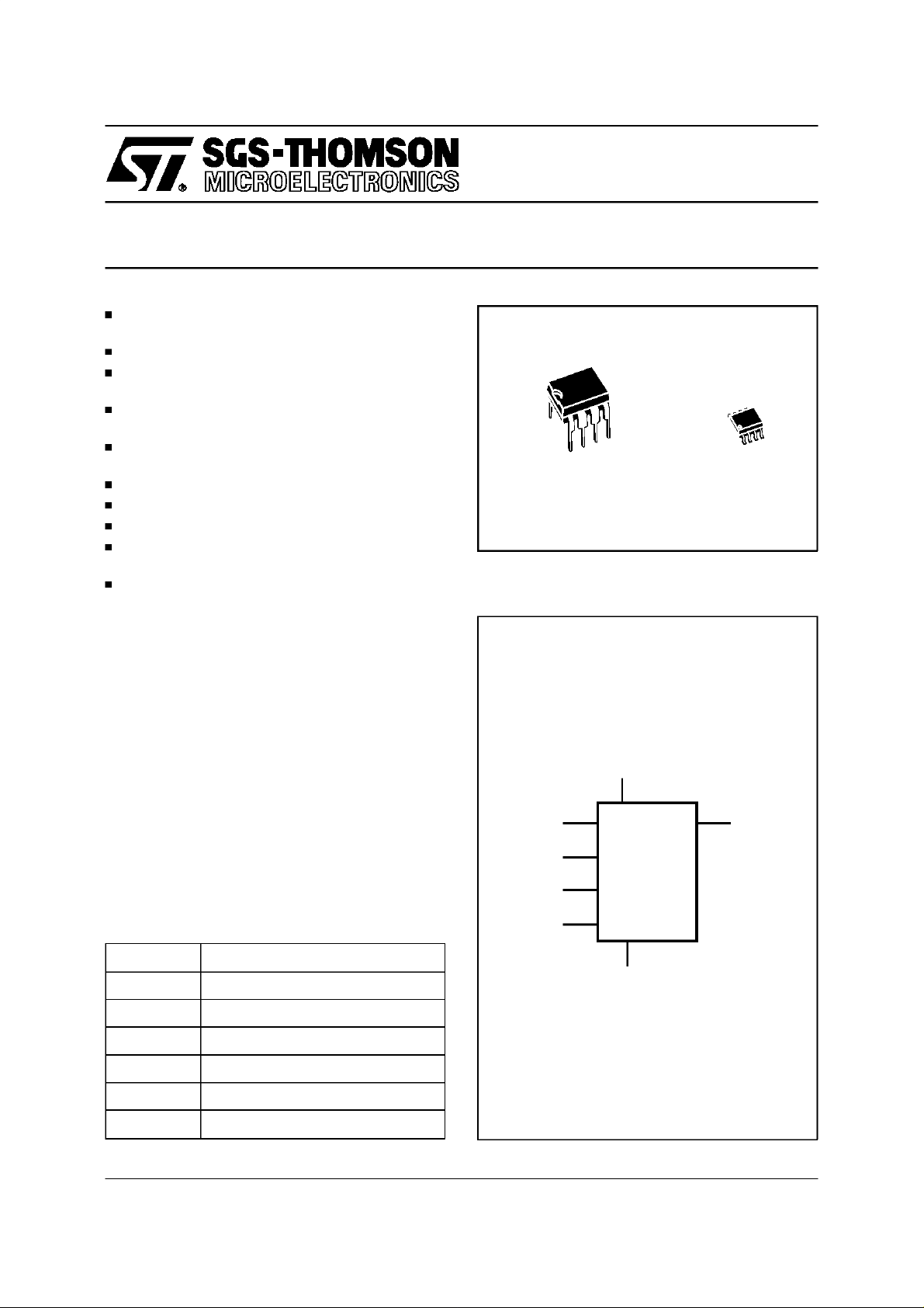
8
1
PSDIP8 (B)
0.4mm Frame
Figure 1. Logic Diagram
8
SO8 (M)
150mil Width
1
DESCRIPTION
The ST93C06 and ST93C06Care 256 bit ElectricallyErasable ProgrammableMemory(EEPROM)
fabricatedwithSGS-THOMSON’sHighEndurance
SinglePolysiliconCMOStechnology.Inthetextthe
two products are referred to as ST93C06.
The memoryis divided into either 32 x 8 bit bytes
or 16 x 16 bit words. The organization may be
selectedby a signalappliedon the ORG input.
The memoryis accessed througha serialinput (D)
and by a set of instructionswhich includes Read a
byte/word, Write a byte/word, Erase a byte/word,
EraseAllandWriteAll. AReadinstructionloadsthe
address of the first byte/word to be read into an
internaladdress pointer.
Table 1. Signal Names
S Chip Select Input
D Serial Data Input
Q Serial Data Output
C Serial Clock
ORG Organisation Select
ORG
V
CC
D
C
S
ST93C06
ST93C06C
V
SS
Q
AI00816B
V
CC
V
SS
June 1997 1/15
This isinformation on a productstill in productionbutnot recommendedfor new designs.
Supply Voltage
Ground
ST93C06,ST93C06C
Figure2A. DIPPin Connections
ST93C06
ST93C06C
SV
1
2
D
3
Q
4
Warning: DU = Don’t Use Warning: DU = Don’t Use
Table 2. Absolute MaximumRatings
Symbol Parameter Value Unit
T
T
T
STG
LEAD
Ambient Operating Temperature –40 to 125 °C
A
Storage Temperature –65 to150 °C
Lead Temperature,Soldering (SO8 package)
8
7
6
5
AI00817B
CC
DUC
ORG
V
SS
(1)
(PSDIP8 package)
Figure2B. SOPin Connections
ST93C06
ST93C06C
1
SV
2
D
3
Q
4
40 sec
10 sec
8
7
6
5
AI00818C
215
260
CC
DUC
ORG
V
SS
°C
V
V
CC
V
ESD
Notes: 1. Exceptfor the rating ”Operating Temperature Range”, stresses above those listed in the Table ”Absolute Maximum Ratings”
DESCRIPTION (cont’d)
Input or Output Voltages(Q = VOHor Hi-Z) –0.3 to VCC+0.5 V
IO
Supply Voltage –0.3 to 6.5 V
Electrostatic Discharge Voltage (Human Body model)
Electrostatic Discharge Voltage (Machine model)
may cause permanent damage to the device. These are stressratings only and operation of thedevice at these or any other
conditions abovethose indicated in the Operating sections of this specification is not implied. Exposure toAbsolute Maximum
Rating conditions for extended periods may affect device reliability.Refer also to the SGS-THOMSON SURE Program and other
relevant quality documents.
2. MIL-STD-883C, 3015.7(100pF, 1500 Ω).
3. EIAJ IC-121 (Condition C) (200pF, 0 Ω).
(2)
ST93C06
ST93C06C
(3)
ST93C06
ST93C06C
2000
4000
500
500
signal on C input may be disconnected or left
running after the start of a Write cycle) and does
The data containedat this addressis then clocked
out serially. The address pointer is automatically
incrementedafterthedata isoutputand,ifthe Chip
Select input (S) is held High, the ST93C06 can
output a sequentialstream of data bytes/words. In
thisway,the memorycanbe readas a datastream
from 8 to 256 bits long, or continuously as the
address counter automatically rolls over to ’00’
when the highest address is reached. Programming is internally self-timed (the external clock
notrequirean erasecyclepriorto the Writeinstruc-
tion. The Writeinstructionwrites 8or 16 bits at one
time into oneof the 32 bytes or 16 words. After the
startoftheprogrammingcycle aBusy/Readysignal
is available on the Data output (Q) when Chip
Select(S) is driven High.
The design of the ST93C06 and the High Endur-
anceCMOStechnologyusedforitsfabricationgive
an Erase/Write cycle Enduranceof 1,000,000cy-
clesand a data retention of 40 years.
V
V
2/15
ST93C06, ST93C06C
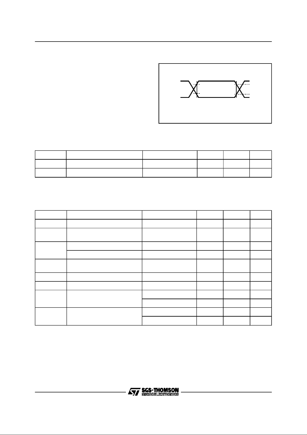
AC MEASUREMENT CONDITIONS
Figure 3. ACTesting Input Output Waveforms
Input Rise and Fall Times ≤ 20ns
Input Pulse Voltages 0.4V to 2.4V
Input Timing Reference Voltages 1V to 2.0V
Output Timing Reference Voltages 0.8V to 2.0V
Note that Output Hi-Z is defined as the point where data
2.4V
0.4V
2V
1V
INPUT OUTPUT
is no longer driven.
Table 3. Capacitance
(1)
(TA=25°C, f =1 MHz)
Symbol Parameter Test Condition Min Max Unit
C
IN
C
OUT
Note: 1. Sampled only, not 100% tested.
Input Capacitance VIN=0V 5 pF
Output Capacitance V
=0V 5 pF
OUT
Table 4. DC Characteristics
= 0 to70°C or –40 to 85°C; VCC=5V±10%)
(T
A
Symbol Parameter TestCondition Min Max Unit
I
I
I
CC1
V
V
V
V
I
LI
LO
CC
IL
IH
OL
OH
Input Leakage Current 0V ≤ VIN≤ V
Output Leakage Current
0V ≤ V
≤ VCC,
OUT
Q inHi-Z
CC
±2.5 µA
±2.5 µA
Supply Current (TTL Inputs) S = VIH, f = 1 MHz 3 mA
Supply Current (CMOS Inputs) S = V
Supply Current (Standby)
, f = 1 MHz 2 mA
IH
,C=VSS,
S=V
SS
ORG = V
SS
or V
CC
50 µA
Input Low Voltage (D, C, S) –0.3 0.8 V
Input High Voltage (D, C, S) 2 VCC+1 V
I
= 2.1mA 0.4 V
Output Low Voltage
Output High Voltage
OL
=10µA 0.2 V
I
OL
I
= –400µA 2.4 V
OH
= –10µAV
I
OH
–0.2 V
CC
2.0V
0.8V
AI00815
3/15
ST93C06,ST93C06C
Table 5. AC Characteristics
(T
= 0 to70°C or –40 to 85°C; VCC=5V±10%)
A
Symbol Alt Parameter Test Condition Min Max Unit
t
SHCH
t
CLSH
t
DVCH
t
CHDX
t
t
t
t
Chip Select High to Clock High 50 ns
CSS
Clock Low to Chip Select High 100 ns
SKS
Input Valid to Clock High 100 ns
DIS
Temp.Range: grade 1 100 ns
Clock High to Input Transition
DIH
Temp.Range:
grades 3, 6
200 ns
t
CHQL
t
CHQV
t
CLSL
t
SLCH
t
SLSH
t
SHQV
t
SLQZ
t
PD0
t
PD1
t
CSH
t
t
t
Clock High to Output Low 500 ns
Clock High to Output Valid 500 ns
Clock Low to Chip Select Low 0 ns
Chip Select Low to ClockHigh 250 ns
Chip Select Low to Chip Select High Note 1 250 ns
CS
Chip Select High to Output Valid 500 ns
SV
Chip Select Low to Output Hi-Z
DF
ST93C06 300 ns
ST93C06C 200 ns
t
CHCL
t
CLCH
t
W
f
C
Notes: 1. Chip Select must bebrought low for a minimum of 250 ns(t
2. The Clock frequency specification calls for aminimum clock period of 1 µs, therefore the sum of the timings t
t
t
must be greater or equal to 1 µs. For example, ift
Clock High to Clock Low Note 2 250 ns
SKH
Clock Low to Clock High Note 2 250 ns
SKL
t
Erase/Write Cycle time 10 ms
WP
f
Clock Frequency 0 1 MHz
SK
) betweenconsecutive instructioncycles.
SLSH
is 250 ns, then t
CHCL
must be at least 750ns.
CLCH
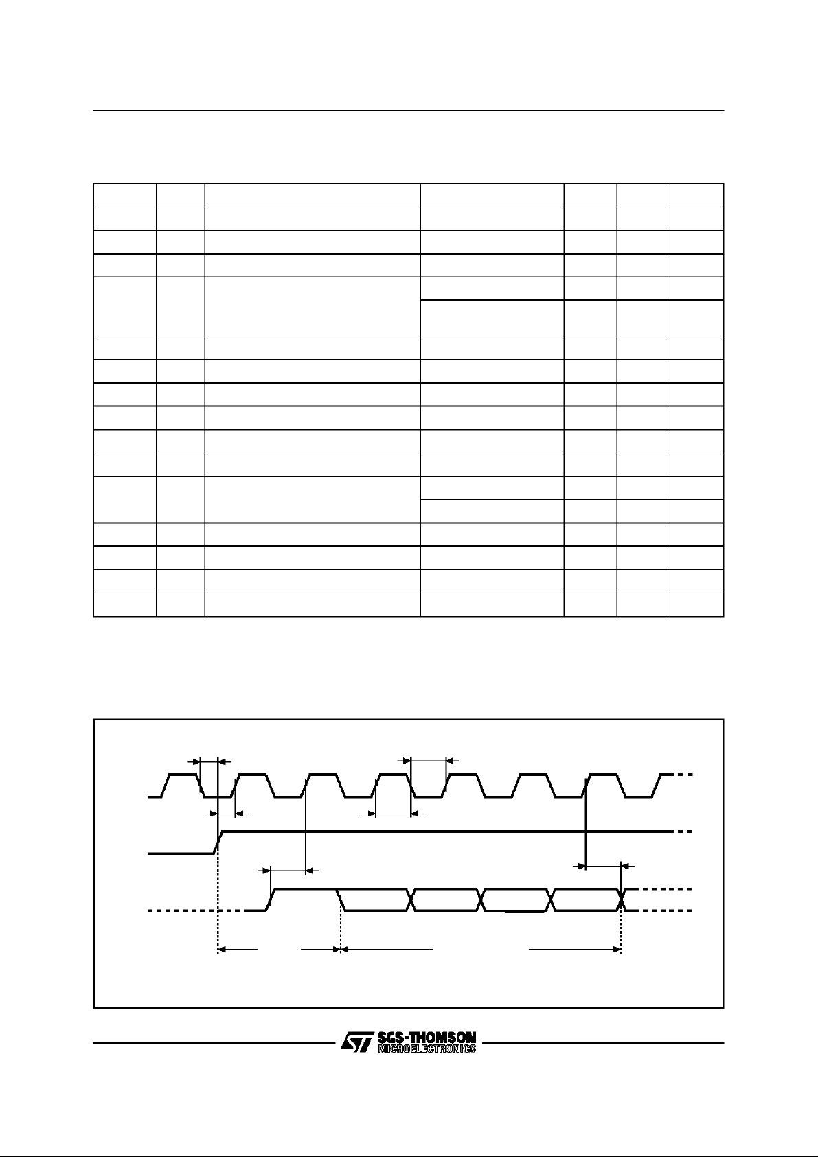
Figure4. SynchronousTiming,Start and Op-Code Input
CHCL+tCLCH
4/15
tCLSH
C
tSHCH
S
tDVCH
D
START
START
OP CODE
OP CODE OP CODE OP CODE
tCLCH
tCHCL
tCHDX
OP CODE INPUT
AI00819C
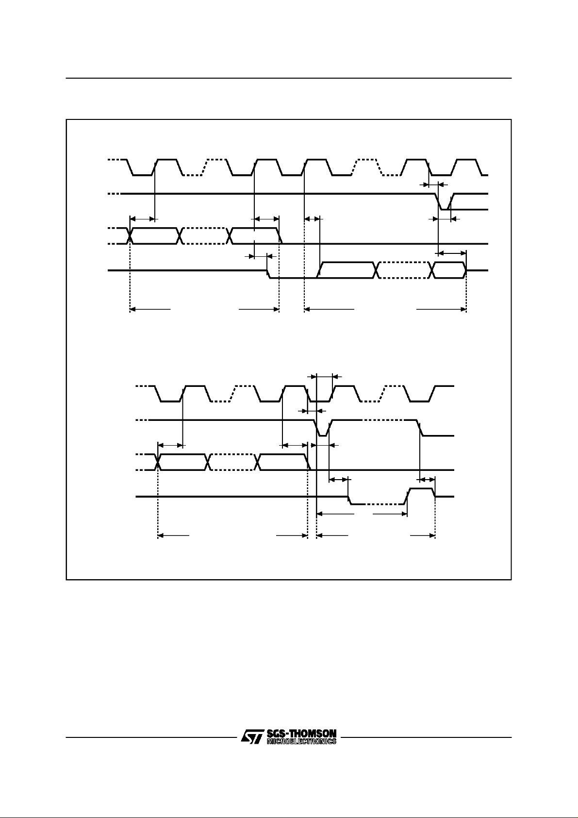
Figure5. Synchronous Timing,Read or Write
C
S
ST93C06, ST93C06C
tCLSL
tDVCH
D
Q
C
S
D
Q
Hi-Z
An
tCHQL
ADDRESS INPUT
tDVCH
An
Hi-Z
A0
A0/D0
tCHQVtCHDX
tSLQZ
Q15/Q7 Q0
DATA OUTPUT
tSLCH
tCLSL
tSLSHtCHDX
BUSY
tSLQZ
READY
tSHQV
tSLSH
AI00820C
ADDRESS/DATA INPUT
DESCRIPTION (cont’d)
TheDU (Don’tUse) pindoesnotaffectthefunction
of the memory and it is reserved for use by SGSTHOMSONduringtest sequences.The pinmay be
left unconnected or may be connected to V
. Direct connection of DU to VSSis recom-
V
SS
CC
or
mended for the lowest standby power consumption.
tW
WRITE CYCLE
AI01429
MEMORYORGANIZATION
The ST93C06is organized as 32 bytes x 8 bits or
16 words x 16 bits. If the ORGinput is left uncon-
nected (or connectedto V
) the x16organization
CC
is selected, when ORG is connected to Ground
) the x8 organization is selected. When the
(V
SS
ST93C06 is in standby mode, the ORG input
shouldbe unconnectedor set to either V
SS
or V
CC
in order to achieve the minimum power consump-
tion. Any voltage between V
and VCCappliedto
SS
ORG may increase the standby current value.
5/15
 Loading...