

SGS Thomson Microelectronics ST92R195B, ST92R195 Datasheet
ON-SCREEN-DISPLAY AND TELETEXT DATA SLICER
■ Register File based 8/16 bit Core Architecture
with RUN, WFI, SLOW and HALT modes
■ 0°C to +70°C Operating Temperature Range
available
■ Up to 24 MHz Operation @ 5V±10%
■ Minimum instruction cycle time: 375ns at
16 MHz internal clock
■ 4 Mbytes address space
■ 256 BytesRAMof Register file(accumulatorsor
index registers)
■ 1024 Bytes of on-chip static RAM
■ 8K Bytes of TDSRAM (Teletext and Display
Storage RAM)
■ 80-lead QFP package
■ 23 fully programmable I/O pins
■ Serial Peripheral Interface
■ Flexible Clock controller for OSD, Data Slicer
and Core clocks running from one single low
frequency external crystal.
■ Enhanced Display Controller with 26 rows of
40/80 characters
– Serial and Parallel attributes
– 10x10 dot Matrix, 512ROM characters, defin-
able by user
– 4/3 and 16/9 supported in 50/60Hz and 100/
120 Hz mode
– Rounding, fringe, double width, doubleheight,
scrolling, cursor, full background color, halfintensity color, translucency and half-tone
modes
■ Teletext unit, including Data slicer, Acquisition
Unit and 8 Kbytes TDSRAM for DataStorage
■ VPS and Wide Screen Signalling slicer
■ Integrated Sync Extractor and Sync Controller
■ 14-bit Voltage Synthesis for tuning reference
voltage
■ Up to 8 ExternalInterrupts plus 1 non-maskable
interrupt
ST92R195B
ROMLESS HCMOS MCU WITH
DATA BRIEFING
QFP80
■ 8 x 8-bit programmable PWM outputs with 5V
open-drain or push-pull capability
■ 16-bit Watchdog timerwith 8-bit prescaler
■ One 16-bit standard timer with 8-bit prescaler
■ 4-channel Analog-to-Digital converter; 5-bit
guaranteed
■ Rich instruction set and 14-Addressing modes
Versatile Development Tools, including Assembler, Linker, C-compiler, Archiver, Source Level
Debugger and Hardware Emulators with RealTime Operating System available from third parties
Device Summary
Device
ST92R195B9 ROMLESS 8K Yes PQFP80
Program
Memory
TDS
RAM
VPS/
WSS
Package
Rev. 2.2
January 2000 1/18
1

ST92R195B - GENERAL DESCRIPTION
1 GENERAL DESCRIPTION
1.1 INTRODUCTION
The ST92R195B microcontroller is developed and
manufactured by STMicroelectronics using a proprietary n-well HCMOS process. Its performance
derives from the use of aflexible 256-register programming model for ultra-fast context switching
and real-time event response. The intelligent onchip peripherals offload the ST9 core from I/O and
data management processing tasks allowing critical application tasks to get the maximum use of
core resources. The ST92R195B MCU supports
low power consumption and low voltage operation
for power-efficient and low-cost embedded systems.
1.1.1 ST9+ Core
The advanced Core consists of the Central
Processing Unit (CPU), the Register File and the
Interrupt controller.
The general-purpose registers canbe used as accumulators, index registers, or address pointers.
Adjacent registerpairs make up 16-bit registersfor
addressing or 16-bit processing. Although the ST9
has an 8-bit ALU, the chip handles 16-bit operations, including arithmetic, loads/stores, and memory/register and memory/memory exchanges.
Two basic addressable spaces are available: the
Memory space and the Register File, which includes the control and status registers of the onchip peripherals.
1.1.2 Power Saving Modes
To optimize performance versus power consumption, a range of operating modes can be dynamically selected.
Run Mode. This is the full speed execution mode
with CPU and peripherals running at the maximum
clock speed delivered by the Phase Locked Loop
(PLL) of the Clock Control Unit(CCU).
Wait For Interrupt Mode. The Wait For Interrupt
(WFI) instruction suspends program execution until an interrupt request is acknowledged. During
WFI, the CPU clock is halted while the peripheral
and interrupt controller keep running at a frequen-
cy programmable via the CCU. In this mode, the
power consumption of the device can be reduced
by more than 95% (LP WFI).
Halt Mode. When executing the HALT instruction,
and if the Watchdog is not enabled, the CPU and
its peripherals stop operating and the status of the
machine remains frozen (the clock is also
stopped). A reset is necessary to exit from Halt
mode.
1.1.3 I/O Ports
Up to 23 I/O lines are dedicated to digital Input/
Output. Theselines are grouped into up to five I/O
Ports and can be configured on a bit basis under
software control to provide timing, status signals,
timer and output,analog inputs, external interrupts
and serial or parallel I/O.
1.1.4 TV Peripherals
A set of on-chip peripherals form a complete system for TV set and VCR applications:
– Voltage Synthesis
– VPS/WSS Slicer
– Teletext Slicer
– Teletext Display RAM
– OSD
1.1.5 On Screen Display
The humaninterface isprovided bythe On Screen
Display module, this can produce up to 26 lines of
up to80 characters from a ROM defined 512 character set. The character resolution is 10x10 dots.
Four character sizes are supported. Serial attributes allow the user to select foreground and
background colours, character size and fringe
background. Parallel attributes can be used toselect additional foreground and background colors
and underline on a character by character basis.
1.1.6 Teletext and Display RAM
The internal 8k Teletext and Display storage RAM
can be usedto store Teletextpages as wellas Display parameters.
2/18

INTRODUCTION (Cont’d)
1.1.7 Teletext, VPS and WSS Data Slicers
The three on-board data slicers using a single external crystal are used toextract the Teletext,VPS
and WSS information from the video signal. Hardware Hamming decoding is provided.
1.1.8 Voltage Synthesis Tuning Control
14-bit Voltage Synthesis using the PWM (Pulse
Width Modulation)/BRM (Bit Rate Modulation)
technique canbeused to generate tuning voltages
for TV set applications. The tuning voltage is output on one of two separate output pins.
1.1.9 PWM Output
Control ofTV settings isable tobe made withup to
eight 8-bit PWM outputs, with a frequency maximum of 23,437Hz at 8-bitresolution (INTCLK = 12
MHz). Low resolutions with higher frequencyoperation can be programmed.
ST92R195B - GENERAL DESCRIPTION
1.1.10 Serial Peripheral Interface (SPI)
The SPI bus is used to communicate with external
devices via the SPI, or I C bus communication
standards. The SPI uses a single line for data input and output. A second line is used for a synchronous c lock signal.
1.1.11 Standard Timer (STIM)
The ST92R195B has one Standard Timer that includes a programmable 16-bit down counter and
an associated 8-bit prescalerwith Single and Continuous counting modes.
1.1.12 Analog/Digital Converter (ADC)
In a ddition there is a 4 channel Analog t o Digital
Converter with integral s ample and hold, fast
5.75µs conversion time and 6-bit guaranteed resolution.
3/18
ST92R195B - GENERAL DESCRIPTION
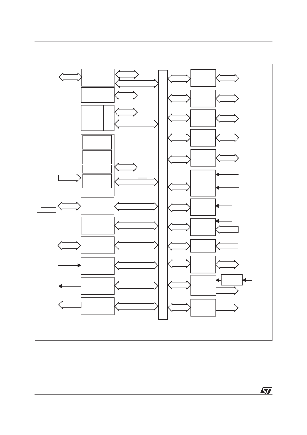
Figure 1. ST92R195B Block Diagram
ADDR[15:0]
DAT[7:0]
ASN
RWN
DSN
MMU[5:0]
External
Memory I/F
1 Kbyte
RAM
I/O
PORT 0
I/O
PORT 2
P0[2:0]
3
P2[5:0]
6
NMI
INT[7:0]
OSCIN
OSCOUT
RESET
RESETO
SDO/SDI
SCK
MCFM
STOUT
VSO[2:1]
8 Kbytes
TDSRAM
256 bytes
Register File
Management
ST9+ CORE
WATCHDOG
TIMING AND
CLOCK CTRL
STANDARD
VOLTAGE
SYNTHESIS
TRI
8/16-bit
CPU
MMU
Interrupt
RCCU
16-BIT
TIMER/
SPI
TIMER
MEMORY BUS
REGISTER BUS
I/O
PORT 3
I/O
PORT 4
I/O
PORT 5
DATA
SLICER
& ACQUI-
SITION
UNIT
SYNC.
EXTRAC-
TION
VPS/WSS
DATA
SLICER
ADC
SYNC
CONTROL
ON
SCREEN
DISPLAY
PWM
D/A CON-
VERTER
4
8
2
FREQ.
MULTIP.
P3[7:4]
P4[7:0]
P5[1:0]
TXCF
CVBS1
WSCR
WSCF
CVBS2
AIN[4:1]
EXTRG
VSYNC
HSYNC/CSYNC
CSO
PXFM
R/G/B/FB
TSLU
HT
PWM[7:0]
4/18
All alternate functions
(Italic characters)
are mapped on Ports 0, 2, 3, 4 and 5

1.2 PIN DESCRIPTION
ST92R195B - GENERAL DESCRIPTION
ADDR[15:0] External memory interface address
bus.
CVBS1 Composite video input signal for the Tele-
text slicer and sync extraction.
CVBS2 Composite video input signal for the VPS/
WSS slicer. Pin AC coupled.
CVBSO, JTDO, JTCK Test pins: leave floating.
DAT[7:0] External memory interface data bus.
DSN Data strobe for external memory interface.
FB
Fast Blanking
. Video analog DAC output.
GND Digital circuit ground.
GNDA Analog circuit ground (must be tied exter-
nally to digital GND).
GNDM External memory interface ground.
HSYNC/CSYNC
Horizontal/Composite sync
. Horizontal or composite video synchronisation input to
OSD. Positive or negative polarity.
JTRST0 Test pin: must be tied to GND.
MCFM Analog pin for the display pixel frequency
multiplier.
MMU[5:0] External memory interface MMU seg-
ment bus
OSCIN, OSCOUT
Oscillator
(input and output).
These pins connect a parallel-resonant crystal
(24MHz maximum), or an external source to the
on-chip clock oscillator and buffer. OSCIN is the
input of the oscillator inverter and internal clock
generator; OSCOUT is the output of the oscillator
inverter.
PXFM Analog pin for the Display Pixel Frequency
Multiplier
RESET
Reset
(input, active low). The ST9+ is ini-
tialised by the Reset signal. With the deactivation
of RESET, program execution begins from the
Program memory location pointed to by the vector
contained in program memory locations 00h and
01h.
R/G/B
Red/Green/Blue
. Video color analog DAC
outputs.
RWN Read/Write strobe for external memory in-
terface.
TEST0 Test pin: must be tied to V
DDA
.
TXCF Analog pin for the teletext PLL.
VDDMainpower supply voltage (5V ±10%, digital)
V
Analog power supply (must be tied external-
DDA
ly to V
V
DDM
VSYNC
).
DDA
External memory interface power supply.
Vertical Sync
. Vertical video synchronisa-
tion input to OSD. Positive or negative polarity.
WSCF, WSCR Analog pins for the VPS/WPP slic-
er. These pins must be tied to ground or not connected.
P0[2:0], P2[5:0], P3[7:4], P4[7:0], P5[1:0]-
Port Lines
(Input/Output, TTL or CMOS compati-
I/O
ble). 23 lines grouped into I/O ports, bit programmable as general purpose I/Oor as Alternate functions (see I/O section).
Important
: Note that open-drain outputs are for
logic levels only and arenot true open drain.
1.2.1 I/O Port Alternate Functions.
Each pin of the I/O ports of the ST92R195B may
assume software programmable Alternate Functions as shown in the Pin Configuration drawings.
Table 1. shows the Functions allocated to eachI/O
Port pin.
5/18
ST92R195B - GENERAL DESCRIPTION
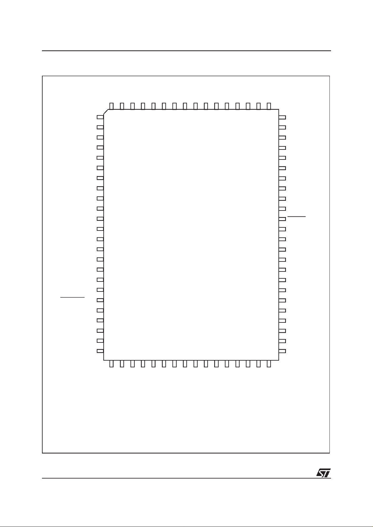
Figure 2. 80-Pin Package Pin-Out
ADDR15
ADDR12
ADDR7
ADDR6
ADDR5
ADDR4
80 79 78 77 76 75 74 73 72 71 70 69 68 67 66 65
MMU0
MMU3
ADDR10
DSN
ADDR11
ADDR9
ADDR8
RWN
GNDM
V
DDM
OSCIN
OSCOUT
ADDR13
ADDR14
MMU1
MMU2
MMU4
MMU5
CSO/RESETO/P3.7
ASN/P3.6
P3.5
P3.4
SDI/SDO/INT1/P5.1
SCK/INT2/P5.0
1
2
3
4
5
6
7
8
9
10
11
12
13
14
15
16
17
18
19
20
21
22
23
24
25 26 27 28 29 30 31 32 37 38 39
ADDR3
ADDR2
33 34 35 36
ADDR1
ADDR0
DAT0
DAT1
DAT2
DAT7
DAT6
40
DAT5
DAT4
64
63
DAT3
62
GNDA
61
CVBS1
60
CVBS2
59
TEST0
58
CVBSO
57
TXCF
56
JTRST0
55
MCFM
54
RESET
53
PXFM
52
VDDA
51
WSCF
50
WSCR
49
HSYNC/CSYNC
VSYNC
48
R
47
G
46
B
45
FB
44
P4.0/PWM0
43
P4.1/PWM1
42
41
P4.2/PWM2
6/18
INT7/P2.0
NMI/P2.4
INT6/VSO1/P2.3
P0.1
AIN4/P0.2
DD
P0.0
PWM6/P4.6
PWM7/EXTRG/INT3/STOUT/P4.7
V
GND
PWM5/P4.5
INT5/AIN1/P2.1
PWM4/P4.4
INT0/AIN2/P2.2
INT4/AIN3/VSO2/P2.5
PWM3/TSLU/HT/P4.3
 Loading...