

SGS Thomson Microelectronics ST92P141K4M6, ST92P141K4B6, ST92P141 Datasheet
October 2001 1/179
Rev. 1.7
ST92141
8/16-BIT MCU FOR 3-PHASE AC MOTOR CONTROL
■ Register File based 8/16 b it Core Architecture
with RUN, WFI, SLOW, HALT and STOP
modes
■ 0-25 MHz Operation (internal clock) @ 5V±10%
voltage range
■ -40°C to +85°C Operating Temperature Range
■ Fully Programmable PLL Clock Generator, with
Frequency Multiplication and low frequency,
low cost external crystal (3-5 MHz)
■ Minimum Instruction Cycle time: 160 ns - (@ 25
MHz internal clock frequency)
■ Internal Memory:
– EPROM/OTP/FA STR OM 16K bytes
– RAM 512 bytes
■ 224 general purpose registers available as RAM,
accumulators or index pointers (register file)
■ 32-pin Dual Inline and 34-pin Small Outline
Packages
■ 15 programmable I/O pins wi th Schmitt Trigger
input, including 4 high sink outputs (20mA @
V
OL
=3V)
■ 4 Wake-up Interrupts (one usable as Non-
Maskable Interrupt) for emergency event
management
■ 3-phase Induction Motor Controller (IMC)
Peripheral with 3 pairs of PWM outputs and
asynchronous emergency stop
■ Serial Peripheral Interface (SPI) with Master/
Slave Mode capability
■ 16-bit Timer with 8-bit Prescaler usable as a
Watchdog Timer
■ 16-bit Standard Timer with 8-bit Prescaler
■ 16-bit Extended Function Timer with Prescaler, 2
Input Captures and 2 Output Compares
■ 8-bit Analog to Di gital Converter allow ing up to
6 input channels with autoscan and watchdog
capabili ty
■ Low Voltage Detector Reset
■ Rich Instruction Set with 14 Addressing Modes
■ Division-by-Zero trap generation
■ Versatile Development Tools, including
Assembler, Linker, C-compiler, Archiver,
Source Level Debugger and Hardware
Emulators with Real-Time Operating System
available from Third Parties
DEVICE SUMMARY
DEVICE
Program
Memory
(Bytes)
RAM
(Bytes)
PACKAGE
ST92P141 16K FASTROM 512
PSDIP32/
SO34
ST92E141 16K EPROM 512 CSDIP32W
ST92T141 16K OTP 512
PSDIP32/
SO34
PSDIP32
SO34 Shrink
CSDIP32W
9

2/179
Table of Contents
179
1
1 GENERAL DESCRIPTION . . . . . . . . . . . . . . . . . . . . . . . . . . . . . . . . . . . . . . . . . . . . . . . . . . . . . . 6
1.1 INTRODUCTION . . . . . . . . . . . . . . . . . . . . . . . . . . . . . . . . . . . . . . . . . . . . . . . . . . . . . . . . . 6
1.1.1 ST9+ Core . . . . . . . . . . . . . . . . . . . . . . . . . . . . . . . . . . . . . . . . . . . . . . . . . . . . . . . . 6
1.1.2 Power Saving Modes . . . . . . . . . . . . . . . . . . . . . . . . . . . . . . . . . . . . . . . . . . . . . . . . 6
1.1.3 System Clock . . . . . . . . . . . . . . . . . . . . . . . . . . . . . . . . . . . . . . . . . . . . . . . . . . . . . . 6
1.1.4 Low Voltage Reset . . . . . . . . . . . . . . . . . . . . . . . . . . . . . . . . . . . . . . . . . . . . . . . . . . 7
1.1.5 I/O Ports . . . . . . . . . . . . . . . . . . . . . . . . . . . . . . . . . . . . . . . . . . . . . . . . . . . . . . . . . . 7
1.1.6 3-ph ase Induction Motor Controller . . . . . . . . . . . . . . . . . . . . . . . . . . . . . . . . . . . . . 7
1.1.7 Watchdog Timer (WDT) . . . . . . . . . . . . . . . . . . . . . . . . . . . . . . . . . . . . . . . . . . . . . . 7
1.1.8 Standard Timer . . . . . . . . . . . . . . . . . . . . . . . . . . . . . . . . . . . . . . . . . . . . . . . . . . . . . 7
1.1.9 Ex tended Funct ion Time r . . . . . . . . . . . . . . . . . . . . . . . . . . . . . . . . . . . . . . . . . . . . . 7
1.1.10 Serial Peripheral Interface (SPI) . . . . . . . . . . . . . . . . . . . . . . . . . . . . . . . . . . . . . . . . 7
1.1.11 Analog/Digital Converter (ADC) . . . . . . . . . . . . . . . . . . . . . . . . . . . . . . . . . . . . . . . . 7
1.2 PIN DESCRIPTION . . . . . . . . . . . . . . . . . . . . . . . . . . . . . . . . . . . . . . . . . . . . . . . . . . . . . . . 9
1.2.1 I/O Port Configuration . . . . . . . . . . . . . . . . . . . . . . . . . . . . . . . . . . . . . . . . . . . . . . . 11
1.2.2 I/O Port Reset State . . . . . . . . . . . . . . . . . . . . . . . . . . . . . . . . . . . . . . . . . . . . . . . . 11
1.3 MEMORY MAP . . . . . . . . . . . . . . . . . . . . . . . . . . . . . . . . . . . . . . . . . . . . . . . . . . . . . . . . . 14
1.3.1 Memory Configuration . . . . . . . . . . . . . . . . . . . . . . . . . . . . . . . . . . . . . . . . . . . . . . 14
1.3.2 EPROM Programming . . . . . . . . . . . . . . . . . . . . . . . . . . . . . . . . . . . . . . . . . . . . . . 14
1.4 REGISTER MAP . . . . . . . . . . . . . . . . . . . . . . . . . . . . . . . . . . . . . . . . . . . . . . . . . . . . . . . . 15
2 DEVICE ARCHITECTURE . . . . . . . . . . . . . . . . . . . . . . . . . . . . . . . . . . . . . . . . . . . . . . . . . . . . . 20
2.1 CORE ARCHITECTURE . . . . . . . . . . . . . . . . . . . . . . . . . . . . . . . . . . . . . . . . . . . . . . . . . . 20
2.2 MEMORY SPACES . . . . . . . . . . . . . . . . . . . . . . . . . . . . . . . . . . . . . . . . . . . . . . . . . . . . . . 20
2.2.1 Register File . . . . . . . . . . . . . . . . . . . . . . . . . . . . . . . . . . . . . . . . . . . . . . . . . . . . . . 20
2.2.2 Register Addressing . . . . . . . . . . . . . . . . . . . . . . . . . . . . . . . . . . . . . . . . . . . . . . . . 22
2.3 SYSTEM REGISTERS . . . . . . . . . . . . . . . . . . . . . . . . . . . . . . . . . . . . . . . . . . . . . . . . . . . . 23
2.3.1 Central Interrupt Control Register . . . . . . . . . . . . . . . . . . . . . . . . . . . . . . . . . . . . . . 23
2.3.2 Flag Register . . . . . . . . . . . . . . . . . . . . . . . . . . . . . . . . . . . . . . . . . . . . . . . . . . . . . 24
2.3.3 Reg ister Pointing Techn iques . . . . . . . . . . . . . . . . . . . . . . . . . . . . . . . . . . . . . . . . . 25
2.3.4 Paged Registers . . . . . . . . . . . . . . . . . . . . . . . . . . . . . . . . . . . . . . . . . . . . . . . . . . . 28
2.3.5 Mode Regi ster . . . . . . . . . . . . . . . . . . . . . . . . . . . . . . . . . . . . . . . . . . . . . . . . . . . . 28
2.3.6 Stack Pointers . . . . . . . . . . . . . . . . . . . . . . . . . . . . . . . . . . . . . . . . . . . . . . . . . . . . . 29
2.4 MEMORY ORGANIZATION . . . . . . . . . . . . . . . . . . . . . . . . . . . . . . . . . . . . . . . . . . . . . . . . 31
2.5 MEMORY MANAGEMENT UNIT . . . . . . . . . . . . . . . . . . . . . . . . . . . . . . . . . . . . . . . . . . . . 32
2.6 ADDRESS SPACE EXTENSION . . . . . . . . . . . . . . . . . . . . . . . . . . . . . . . . . . . . . . . . . . . . 33
2.6.1 Addressing 16-Kbyte Pages . . . . . . . . . . . . . . . . . . . . . . . . . . . . . . . . . . . . . . . . . . 33
2.6.2 Addressing 64-Kbyte Segments . . . . . . . . . . . . . . . . . . . . . . . . . . . . . . . . . . . . . . . 34
2.7 MMU REGISTERS . . . . . . . . . . . . . . . . . . . . . . . . . . . . . . . . . . . . . . . . . . . . . . . . . . . . . . . 34
2.7.1 DPR[ 3:0]: Data Page Registers . . . . . . . . . . . . . . . . . . . . . . . . . . . . . . . . . . . . . . . 34
2.7.2 CSR: Code Segment Register . . . . . . . . . . . . . . . . . . . . . . . . . . . . . . . . . . . . . . . . 36
2.7.3 ISR: Interrupt Segment Register . . . . . . . . . . . . . . . . . . . . . . . . . . . . . . . . . . . . . . . 36
2.7.4 DMASR: DMA Segment Register . . . . . . . . . . . . . . . . . . . . . . . . . . . . . . . . . . . . . . 36
2.8 MMU USAGE . . . . . . . . . . . . . . . . . . . . . . . . . . . . . . . . . . . . . . . . . . . . . . . . . . . . . . . . . . . 38
2.8.1 Normal Program Execution . . . . . . . . . . . . . . . . . . . . . . . . . . . . . . . . . . . . . . . . . . . 38
2.8.2 Interrupts . . . . . . . . . . . . . . . . . . . . . . . . . . . . . . . . . . . . . . . . . . . . . . . . . . . . . . . . . 38
2.8.3 DMA . . . . . . . . . . . . . . . . . . . . . . . . . . . . . . . . . . . . . . . . . . . . . . . . . . . . . . . . . . . . 38
3 INTERRUPTS . . . . . . . . . . . . . . . . . . . . . . . . . . . . . . . . . . . . . . . . . . . . . . . . . . . . . . . . . . . . . . . 39
3.1 INTRODUCTION . . . . . . . . . . . . . . . . . . . . . . . . . . . . . . . . . . . . . . . . . . . . . . . . . . . . . . . . 39

3/179
Table of Contents
3.2 INTERRUPT VECTORING . . . . . . . . . . . . . . . . . . . . . . . . . . . . . . . . . . . . . . . . . . . . . . . . 39
3.2.1 Divide by Zero trap . . . . . . . . . . . . . . . . . . . . . . . . . . . . . . . . . . . . . . . . . . . . . . . . . 39
3.2.2 Segment Paging During Interrupt Routines . . . . . . . . . . . . . . . . . . . . . . . . . . . . . . 40
3.3 INTERRUPT PRIORITY LEVELS . . . . . . . . . . . . . . . . . . . . . . . . . . . . . . . . . . . . . . . . . . . 40
3.4 PRIORITY LEVEL ARBITRATION . . . . . . . . . . . . . . . . . . . . . . . . . . . . . . . . . . . . . . . . . . . 40
3.4.1 Priority level 7 (Lowest) . . . . . . . . . . . . . . . . . . . . . . . . . . . . . . . . . . . . . . . . . . . . . 40
3.4.2 Maximum depth of nesting . . . . . . . . . . . . . . . . . . . . . . . . . . . . . . . . . . . . . . . . . . . 40
3.4.3 Sim ultaneou s Inte rrupts . . . . . . . . . . . . . . . . . . . . . . . . . . . . . . . . . . . . . . . . . . . . . 40
3.4.4 Dynamic Priority Level Modification . . . . . . . . . . . . . . . . . . . . . . . . . . . . . . . . . . . . 41
3.5 ARBITRATION MODES . . . . . . . . . . . . . . . . . . . . . . . . . . . . . . . . . . . . . . . . . . . . . . . . . . . 41
3.5.1 Concurrent Mode . . . . . . . . . . . . . . . . . . . . . . . . . . . . . . . . . . . . . . . . . . . . . . . . . . 41
3.5.2 Nested Mode . . . . . . . . . . . . . . . . . . . . . . . . . . . . . . . . . . . . . . . . . . . . . . . . . . . . . 44
3.6 EXTERNAL INTERRUPTS . . . . . . . . . . . . . . . . . . . . . . . . . . . . . . . . . . . . . . . . . . . . . . . . 46
3.7 TOP LEVEL INTERRUPT . . . . . . . . . . . . . . . . . . . . . . . . . . . . . . . . . . . . . . . . . . . . . . . . . 48
3.8 ON-CHIP PERIPHERAL INTERRUPTS . . . . . . . . . . . . . . . . . . . . . . . . . . . . . . . . . . . . . . 48
3.9 NMI/WKP0 LINE MANAGEMENT . . . . . . . . . . . . . . . . . . . . . . . . . . . . . . . . . . . . . . . . . . . 49
3.9.1 NMI/Wake-Up Event Handling in Run mode . . . . . . . . . . . . . . . . . . . . . . . . . . . . . 50
3.9.2 NMI/Wake-Up Event Handling in STOP mode . . . . . . . . . . . . . . . . . . . . . . . . . . . . 50
3.9.3 Unused Wake Up Management Unit lines . . . . . . . . . . . . . . . . . . . . . . . . . . . . . . . 50
3.10INTERRUPT RESPONSE TIME . . . . . . . . . . . . . . . . . . . . . . . . . . . . . . . . . . . . . . . . . . . . 51
3.11INTERRUPT REGISTERS . . . . . . . . . . . . . . . . . . . . . . . . . . . . . . . . . . . . . . . . . . . . . . . . . 52
3.12WAKE-UP / INTERRUPT LINES MANAGEMENT UNIT (WUIMU) . . . . . . . . . . . . . . . . . . 55
3.12.1 Introduction . . . . . . . . . . . . . . . . . . . . . . . . . . . . . . . . . . . . . . . . . . . . . . . . . . . . . . . 55
3.12.2 Main Features . . . . . . . . . . . . . . . . . . . . . . . . . . . . . . . . . . . . . . . . . . . . . . . . . . . . . 55
3.12.3 Functional Description . . . . . . . . . . . . . . . . . . . . . . . . . . . . . . . . . . . . . . . . . . . . . . 56
3.12.4 Programming Considerations . . . . . . . . . . . . . . . . . . . . . . . . . . . . . . . . . . . . . . . . . 57
3.12.5 Register Description . . . . . . . . . . . . . . . . . . . . . . . . . . . . . . . . . . . . . . . . . . . . . . . . 59
4 EM CONFIGURATION REGISTERS (EM) . . . . . . . . . . . . . . . . . . . . . . . . . . . . . . . . . . . . . . . . . 62
5 RESET AND CLOCK CONTROL UNIT (RCCU) . . . . . . . . . . . . . . . . . . . . . . . . . . . . . . . . . . . . 63
5.1 INTRODUCTION . . . . . . . . . . . . . . . . . . . . . . . . . . . . . . . . . . . . . . . . . . . . . . . . . . . . . . . . 63
5.2 CLOCK CONTROL UNIT . . . . . . . . . . . . . . . . . . . . . . . . . . . . . . . . . . . . . . . . . . . . . . . . . . 63
5.2.1 Clock Control Unit Overview . . . . . . . . . . . . . . . . . . . . . . . . . . . . . . . . . . . . . . . . . . 63
5.3 CLOCK MANAGEMENT . . . . . . . . . . . . . . . . . . . . . . . . . . . . . . . . . . . . . . . . . . . . . . . . . . 65
5.3.1 PLL Clock Multiplier Programming . . . . . . . . . . . . . . . . . . . . . . . . . . . . . . . . . . . . . 66
5.3.2 CPU Clock Prescaling . . . . . . . . . . . . . . . . . . . . . . . . . . . . . . . . . . . . . . . . . . . . . . 66
5.3.3 Peripheral Clock . . . . . . . . . . . . . . . . . . . . . . . . . . . . . . . . . . . . . . . . . . . . . . . . . . . 66
5.3.4 Low Power Modes . . . . . . . . . . . . . . . . . . . . . . . . . . . . . . . . . . . . . . . . . . . . . . . . . 67
5.3.5 Interrupt Generation . . . . . . . . . . . . . . . . . . . . . . . . . . . . . . . . . . . . . . . . . . . . . . . . 67
5.4 CLOCK CONTROL REGISTERS . . . . . . . . . . . . . . . . . . . . . . . . . . . . . . . . . . . . . . . . . . . . 69
5.5 OSCILLATOR CHARACTERISTICS . . . . . . . . . . . . . . . . . . . . . . . . . . . . . . . . . . . . . . . . . 73
5.6 RESET/STOP MANAGER . . . . . . . . . . . . . . . . . . . . . . . . . . . . . . . . . . . . . . . . . . . . . . . . . 74
5.6.1 Reset Pin Timing . . . . . . . . . . . . . . . . . . . . . . . . . . . . . . . . . . . . . . . . . . . . . . . . . . 75
5.7 STOP MODE . . . . . . . . . . . . . . . . . . . . . . . . . . . . . . . . . . . . . . . . . . . . . . . . . . . . . . . . . . . 76
5.8 LOW VOLTAGE DETECTOR (LVD) . . . . . . . . . . . . . . . . . . . . . . . . . . . . . . . . . . . . . . . . . 78
6 I/O PORTS . . . . . . . . . . . . . . . . . . . . . . . . . . . . . . . . . . . . . . . . . . . . . . . . . . . . . . . . . . . . . . . . . . 79
6.1 INTRODUCTION . . . . . . . . . . . . . . . . . . . . . . . . . . . . . . . . . . . . . . . . . . . . . . . . . . . . . . . . 79
6.2 SPECIFIC PORT CONFIGURATIONS . . . . . . . . . . . . . . . . . . . . . . . . . . . . . . . . . . . . . . . 79

4/179
Table of Contents
179
6.3 PORT CONTROL REGISTERS . . . . . . . . . . . . . . . . . . . . . . . . . . . . . . . . . . . . . . . . . . . . . 79
6.4 INPUT/OUTPUT BIT CONFIGURATION . . . . . . . . . . . . . . . . . . . . . . . . . . . . . . . . . . . . . . 80
6.5 ALTERNATE FUNCTION ARCHITECTURE . . . . . . . . . . . . . . . . . . . . . . . . . . . . . . . . . . . 84
6.5.1 Pin Declared as I/O . . . . . . . . . . . . . . . . . . . . . . . . . . . . . . . . . . . . . . . . . . . . . . . . . 84
6.5.2 Pin Declared as an Alternate Function Input . . . . . . . . . . . . . . . . . . . . . . . . . . . . . 84
6.5.3 Pin Declared as an Alternate Function Output . . . . . . . . . . . . . . . . . . . . . . . . . . . . 84
6.6 I/O STATUS AFTER WFI, HALT AND RESET . . . . . . . . . . . . . . . . . . . . . . . . . . . . . . . . . 84
7 ON-CHIP PERIPHERALS . . . . . . . . . . . . . . . . . . . . . . . . . . . . . . . . . . . . . . . . . . . . . . . . . . . . . . 85
7.1 TIMER/WATCHDOG (WDT) . . . . . . . . . . . . . . . . . . . . . . . . . . . . . . . . . . . . . . . . . . . . . . . 85
7.1.1 Introduction . . . . . . . . . . . . . . . . . . . . . . . . . . . . . . . . . . . . . . . . . . . . . . . . . . . . . . . 85
7.1.2 F unctional Desc ription . . . . . . . . . . . . . . . . . . . . . . . . . . . . . . . . . . . . . . . . . . . . . . 86
7.1.3 Watchdog Timer Operation . . . . . . . . . . . . . . . . . . . . . . . . . . . . . . . . . . . . . . . . . . . 87
7.1.4 WDT Interrupts . . . . . . . . . . . . . . . . . . . . . . . . . . . . . . . . . . . . . . . . . . . . . . . . . . . . 89
7.1.5 Register Description . . . . . . . . . . . . . . . . . . . . . . . . . . . . . . . . . . . . . . . . . . . . . . . . 90
7.2 STANDARD TIMER (STIM) . . . . . . . . . . . . . . . . . . . . . . . . . . . . . . . . . . . . . . . . . . . . . . . . 92
7.2.1 Introduction . . . . . . . . . . . . . . . . . . . . . . . . . . . . . . . . . . . . . . . . . . . . . . . . . . . . . . . 92
7.2.2 F unctional Desc ription . . . . . . . . . . . . . . . . . . . . . . . . . . . . . . . . . . . . . . . . . . . . . . 93
7.2.3 Interrupt Selection . . . . . . . . . . . . . . . . . . . . . . . . . . . . . . . . . . . . . . . . . . . . . . . . . . 94
7.2.4 Register Mapping . . . . . . . . . . . . . . . . . . . . . . . . . . . . . . . . . . . . . . . . . . . . . . . . . . 94
7.2.5 Register Description . . . . . . . . . . . . . . . . . . . . . . . . . . . . . . . . . . . . . . . . . . . . . . . . 95
7.3 EXTENDED FUNCTION TIMER (EFT) . . . . . . . . . . . . . . . . . . . . . . . . . . . . . . . . . . . . . . . 96
7.3.1 Introduction . . . . . . . . . . . . . . . . . . . . . . . . . . . . . . . . . . . . . . . . . . . . . . . . . . . . . . . 96
7.3.2 Main Features . . . . . . . . . . . . . . . . . . . . . . . . . . . . . . . . . . . . . . . . . . . . . . . . . . . . . 96
7.3.3 F unctional Desc ription . . . . . . . . . . . . . . . . . . . . . . . . . . . . . . . . . . . . . . . . . . . . . . 96
7.3.4 Inte rrupt Managem ent . . . . . . . . . . . . . . . . . . . . . . . . . . . . . . . . . . . . . . . . . . . . . 106
7.3.5 Register Description . . . . . . . . . . . . . . . . . . . . . . . . . . . . . . . . . . . . . . . . . . . . . . . 108
7.4 3-PHASE INDUCTION MOTOR CONTROLLER (IMC) . . . . . . . . . . . . . . . . . . . . . . . . . . 116
7.4.1 Introduction . . . . . . . . . . . . . . . . . . . . . . . . . . . . . . . . . . . . . . . . . . . . . . . . . . . . . . 116
7.4.2 Main Features . . . . . . . . . . . . . . . . . . . . . . . . . . . . . . . . . . . . . . . . . . . . . . . . . . . . 116
7.4.3 F unctional Desc ription . . . . . . . . . . . . . . . . . . . . . . . . . . . . . . . . . . . . . . . . . . . . . 116
7.4.4 T acho Count er Operating mod e . . . . . . . . . . . . . . . . . . . . . . . . . . . . . . . . . . . . . . 122
7.4.5 IMC Operating mode . . . . . . . . . . . . . . . . . . . . . . . . . . . . . . . . . . . . . . . . . . . . . . 122
7.4.6 IMC Output selection . . . . . . . . . . . . . . . . . . . . . . . . . . . . . . . . . . . . . . . . . . . . . . 123
7.4.7 NM I manage men t . . . . . . . . . . . . . . . . . . . . . . . . . . . . . . . . . . . . . . . . . . . . . . . . . 124
7.4.8 Register Description . . . . . . . . . . . . . . . . . . . . . . . . . . . . . . . . . . . . . . . . . . . . . . . 125
7.5 SERIAL PERIPHERAL INTERFACE (SPI) . . . . . . . . . . . . . . . . . . . . . . . . . . . . . . . . . . . 135
7.5.1 Introduction . . . . . . . . . . . . . . . . . . . . . . . . . . . . . . . . . . . . . . . . . . . . . . . . . . . . . . 135
7.5.2 Main Features . . . . . . . . . . . . . . . . . . . . . . . . . . . . . . . . . . . . . . . . . . . . . . . . . . . . 135
7.5.3 G eneral Descript ion . . . . . . . . . . . . . . . . . . . . . . . . . . . . . . . . . . . . . . . . . . . . . . . 135
7.5.4 F unctional Desc ription . . . . . . . . . . . . . . . . . . . . . . . . . . . . . . . . . . . . . . . . . . . . . 137
7.5.5 Inte rrupt Managem ent . . . . . . . . . . . . . . . . . . . . . . . . . . . . . . . . . . . . . . . . . . . . . 144
7.5.6 Register Description . . . . . . . . . . . . . . . . . . . . . . . . . . . . . . . . . . . . . . . . . . . . . . . 145
7.6 ANALOG TO DIGITAL CONVERTER (ADC) . . . . . . . . . . . . . . . . . . . . . . . . . . . . . . . . . . 147
7.6.1 Introduction . . . . . . . . . . . . . . . . . . . . . . . . . . . . . . . . . . . . . . . . . . . . . . . . . . . . . . 147
7.6.2 F unctional Desc ription . . . . . . . . . . . . . . . . . . . . . . . . . . . . . . . . . . . . . . . . . . . . . 148
7.6.3 Interrupts . . . . . . . . . . . . . . . . . . . . . . . . . . . . . . . . . . . . . . . . . . . . . . . . . . . . . . . . 150
7.6.4 Register Description . . . . . . . . . . . . . . . . . . . . . . . . . . . . . . . . . . . . . . . . . . . . . . . 151
8 ELECTRICAL CHARACTERISTICS . . . . . . . . . . . . . . . . . . . . . . . . . . . . . . . . . . . . . . . . . . . . . 156

5/179
Table of Contents
9 GENERAL INFORMATION . . . . . . . . . . . . . . . . . . . . . . . . . . . . . . . . . . . . . . . . . . . . . . . . . . . . 174
9.1 PACKAGE MECHANICAL DATA . . . . . . . . . . . . . . . . . . . . . . . . . . . . . . . . . . . . . . . . . . . 174
9.2 ORDERING INFORMATION . . . . . . . . . . . . . . . . . . . . . . . . . . . . . . . . . . . . . . . . . . . . . . 176
9.3 TRANSFER OF CUSTOMER CODE . . . . . . . . . . . . . . . . . . . . . . . . . . . . . . . . . . . . . . . . 176
10 SUMMARY OF CHANGES . . . . . . . . . . . . . . . . . . . . . . . . . . . . . . . . . . . . . . . . . . . . . . . . . . . 178

6/179
ST92141 - GENER AL DESCRIPTION
1 GENERAL DESCRIPTION
1.1 INTRODUCTION
The ST92141 microcontroller is developed and
manufactured by STMicroelec tronics using a proprietary n-well HCMOS process. Its performance
derives from the use of a flexible 256-register programming model for ultra-fast context switching
and real-time event response. The intelligent onchip peripherals offload the ST9 core from I/O and
data management processing tasks al lowing critical application tasks to get the m aximum use of
core resources. The new-generation ST9 MCU
devices now also support low power co nsump tion
and low voltage operation for power-efficient and
low-cost embedded systems.
1.1.1 ST9+ Core
The advanced Core consists of the Central
Processing Unit (CPU), the Register File, the Interrupt controller, and the Memory Management Unit.
The MMU allows addressing of up to 4 Megabytes
of program and data mapped into a sing le linear
space.
Four independent buses are controlled by the
Core: a 16-bit memory bus, an 8 -bit register data
bus, an 8-bit register address bus and a 6-bit interrupt bus which connects the interrupt controllers in
the on-chip peripherals with the core.
Note: The DMA features of the ST9+ core are not
used by the on-chip peripherals of the ST92141.
This multiple bus architecture makes the ST9 family devices highly efficient for accessing on and offchip memory and fast exchange of data with the
on-chip peripherals.
The general-purpose registers can be used as accumulators, index registers, or address pointers.
Adjacent register pairs make up 16-bit registers for
addressing or 16-bit processing. Although the ST9
has an 8-bit ALU, the chip handles 16-bit operations, including arithmetic, loads/stores, and memory/register and memory/memory exchanges.
1.1.2 Power Savin g Modes
To optimize performance versus power consumption, a range of operating modes can be dynamically selected by software according to the requirements of the application.
Run Mode. This is the f ull s pee d execution mod e
with CPU and peripherals running at the maximum
clock speed delivered either by the Phase Locked
Loop controlled by the RCCU (Reset and Clock
Control Unit), directly by the oscillator or by an ex-
ternal source (dedicated Pin or Alternate Function).
Slow Mode. Power consumption can be significantly reduced by running the CPU and the peripherals at reduced clock speed using the CPU Prescaler and RCCU Clock Divider.
Wait For Interrupt Mode. The Wait For Interrupt
(WFI) instruction suspends program execution until an interrupt request is acknowledged. During
WFI, the CPU clock is halted while the peripheral
with interrupt capability and interrupt controller are
kept running at a frequency that can be programmed by software in the RCCU registers. In
this mode, the power consumption of t he device
can be reduced by more than 95% (Low Power
WFI).
Halt Mode. When executing the HALT instruction,
and if the Watchdo g is not enab led, the CP U and
its peripherals stop operating. If however the
Watchdog is enabled, the HALT instruction has no
effect. The main difference between Halt mode
and Stop mode is that a reset is necessary to exit
from Halt mode which causes the system to be
reinitialized.
Stop Mode. When Stop mode is requested by executing the STOP sequenc e (see Wake-up Management Unit section), the CPU and the peripherals stop operating. Operations resume after a
wake-up line is activated. The difference between
Stop mode and Halt mode is in the way the CPU
exits each state: when the STO P sequence is executed, the status of the registers is recorded, and
when the system exits from Stop mo de the CPU
continues execution with the s am e status, without
a system reset.
The Watchdog count er, if enable d, is stop ped. A fter exiting Stop mode it restarts counting from
where it left off.
When the MCU exits from STOP mode, the oscillator, which was also s leeping, requi res a start-up
time to restart working properly. An internal counter is present to guarantee that, after e xiting Stop
Mode, all operations take place with the clock stabilised.
1.1.3 System Clock
A programmable PLL Clock Generator allows
standard 3 to 5 MHz crystals to be used to obtain a
large range of internal frequencies up to 25MHz.
9

7/179
ST92141 - GENERAL DESCRIPTION
1.1.4 Low Voltage Reset
The on-chip Low Voltage Detector (LVD) generates a static reset when the supply voltage is below a reference value. The LVD works both during
power-on as well as when the power supply drops
(brown-out). The reference value for the voltage
drop is lower than the reference value for p oweron in order to avoid a parasitic reset when the
MCU starts running and sinks current on the supply (hysteresis).
1.1.5 I/O Ports
The I/O lines are grouped into two I/O Ports and
can be configured on a bit basis to provide timing,
status signals, an address/data bus for timer inputs and outputs, analog inputs, external wake-up
lines and serial or parallel I/O.
1.1.6 3-phase Induction Motor Controll er
The IMC controller is designed f or variable spee d
motor control applications. Three pairs of PWM
outputs ar e availa ble fo r contro lling a three-ph as e
motor drive. Rotor speed feedba ck is provided by
capturing a tachogenerator input signal. Emergency stop is provided by putting the PWM outputs in
high impedance m ode upon asynchronous faulty
event on NMI pin.
1.1.7 Watchdog Timer (WDT)
The Watchdog timer can be used to m onitor system integrity. When enabled, it generates a reset
after a timeout period unless the counter is refreshed by the application software. For additional
security, watchdog function can be enabled by
hardware using a specific pin.
1.1.8 Standard Timer
The standard timer includes a programmable 16bit down-counter and an associated 8-bit prescaler
with Single and Continuous counting modes.
1.1. 9 E x tended Function Timer
The Extended Func tion Timer can be used for a
wide range of standard timing tasks. It has a 16-bit
free running counter with programmable prescaler. Each timer can have up to 2 input capture and
2 output compare pins wi th associated registers.
This allows applications to measure pulse intervals or generate pulse waveforms. Timer overflow
and other events are f lagged in a status register
with optional interrupt generation.
1.1.10 Serial Peripheral Interface (SPI)
The SPI bus is used to communicate with external
devices via the SPI, or I²C bus communication
standards.
1.1.11 Analog/Digital Converter (ADC)
The ADC provides up to 6 an alog inputs with onchip sample and hold. The analo g watchdog generates an interrupt when the i nput voltage moves
out of a preset threshold.
9
8/179
ST92141 - GENER AL DESCRIPTION
Figure 1. ST92141 Block Diagram
Register File
256 bytes
ST9+ CORE
8/16-bit
CPU
Interrupt
Management
MEMORY BUS
RCCU + LVD
REGISTER BUS
WATCHDOG
MISO
MOSI
SCK
SSN
EF TIMER
SPI
IMC
TACHO
UH
UL
VH
VL
WH
WL
STIN
STOUT
All alternate functions (
Italic characters
) are mapped on Port3 and Port5
Fully Prog.
I/Os
P3[6:0]
P5[7:0]
NMI
WKUP[3:0]
INT0
INT6
OSCIN
OSCOUT
RESET
INTCLK
CK_AF
RAM
512 bytes
EPROM/
FASTROM
16K
A/D Converter
with analog
watchdog
AIN[7:2]
EXTRG
WDIN
WDOUT
STIM TIMER
ICAP1
OCMP1
ICAP2
OCMP2
EXTCLK
9

9/179
ST92141 - GENERAL DESCRIPTION
1.2 PIN DESCRI PTION
ST92E141
134
1817
V
SS
TACHO
VH
VL
WH
WL
UH
UL
N.C.
V
PP
P5.0/WKUP1/ICAP2
P5.1/NMI/WKUP0
RESET
OSCOUT
OSCIN
V
SS
V
DD
PSDIP32/CSDIP32W Package
SO34 Package
ST92E141
132
17
16
V
SS
TACHO
VH
VL
WH
WL
UH
UL
V
PP
P5.0/WKUP1/ICAP2
P5.1/NMI/WKUP0
RESET
OSCOUT
OSCIN
V
SS
V
DD
V
DD
MOSI/P3.0
MISO/P3.1
SCK/STIN/WKUP3/P3.2
STOUT/SSN/P3.3
EXTRG/OCMP2/P3.4
INT6/OCMP1/P3.5
ICAP1/WKUP2/P3.6
AV
DD
AV
SS
INTCLK/AIN7/P5.7
CK_AF/AIN6/P5.6
AIN5/P5.5
AIN4/P5.4
AIN3/EXTCLK/WDO UT/ P5.3
AIN2/INT0/WDIN/P5.2
V
DD
MOSI/P3.0
MISO/P3.1
SCK/STIN/WKUP3 /P 3.2
STOUT/SSN/P3.3
EXTRG/OCMP2/P3.4
INT6/OCMP1/P3.5
ICAP1/WKUP2/P3.6
N.C.
AV
DD
AV
SS
INTCLK/AIN7/P5.7
CK_AF/AIN6/P5.6
AIN5/P5.5
AIN4/P5.4
AIN3/EXTCLK/W DO UT/P5.3
AIN2/INT0/WDIN/P5.2
9
10/179
ST92141 - GENER AL DESCRIPTION
9
Table 1. Power Supply Pins Table 2. Primary Function pins
Name Function
SDIP32
SO34
V
PP
Programming voltage for
EPROM/OTP devices. Must be
connected to V
SS
in user mode.
24 25
V
DD
Main power supply voltage (5V ±
10% (2 pins internally connected)
17 18
11
V
SS
Digital Circuit Ground (2 pins internally connected)
18 19
32 34
AV
DD
Analog V
DD
of the Analog to Digit-
al Converter
910
AV
SS
Analog V
SS
of the Analog to Digit-
al Converter
10 11
Name Function
SDIP32
SO34
TACHO
Signal input from a tachogenerator to the IMC controller for
measuring the rotor speed
31 33
UH U-phase PWM output signal 26 28
VH V-phase PWM output signal 30 32
WH W-phase PWM output signal 28 30
UL The complemented UH, VH, WH
output signals with added dead
time to avoid crossover conduction from the power driver
25 27
VL 29 31
WL 27 29
RESET
Reset (input, active low). The
ST9+ is initialised by the Reset
signal. With the deactivation of
RESET
, program execution begins from the memory location
pointed to by the vector contained in memory locations 00h
and 01h
21 22
OSCIN
OSCIN is the input of the oscillator inverter and internal clock
generator. OSCIN and OSCOUT
connect a parallel-resonant crystal (3 to 5 MHz), or an external
source to the on-chip clock oscillator and buffer
19 20
OSCOUT
OSCOUT is the output of the oscillator inverter
20 21

11/179
ST92141 - GENERAL DESCRIPTION
1.2.1 I/O Port Configuration
All ports can be individually configured as input, bidirectional, output, or alternate function. Refer t o
the Port Bit Configuration Table in the I/O Port
Chapter.
All I/Os are implemented with a High Hysteresis or
Standard Hysteresis Schmitt trigger function (See
Electrical Characteristics).
Weak Pull-Up = This column indicat es if a weak
pull-up is present or not (refer to Table 3).
– If WPU = yes, then the WPU can be enabled/dis-
able by software
– If WPU = no, then enabling the WPU by software
has no effect
All port output configurations can be software selected on a bit basis to provide push-pull or open
drain driving capabilities. For all ports, when configured as open-drain, the voltage on the pin must
never exceed the V
DD
power line value (refer to
Electrical characteristics section).
1.2.2 I/O Port Reset State
I/Os are reset asynchronously as soon as the RESET pin is asserted low.
All I/Os are forced by the Reset in "floating input"
configuration mode.
WARNING
When a com mon p in is de clared to be connect ed
to an alternate function input and to an alternate
function output, the user must be aware of the fact
that the alternate function output signal always inputs to the alternate funct ion module declared as
input.
When any given pin is declared to be connected to
a digital alternate function input, the user must be
aware of the fact that the alternate function input is
always connected to the pin. When a given pin is
declared to be connected to an analog alternate
function input (ADC input for example) and if this
pin is programmed in the "AF-OD" mode, the digital input path is disconnected from the pin t o prevent any DC consumption.
Table 3. I/O Port Characteristics
Legend: OD = Open Drain; HC= High current
Input Output Weak Pull-Up Reset State
Port 3[4:0]
Port 3[6:5]
Schmitt trigger (High Hysteresis)
Schmitt trigger (High Hysteresis)
Push-Pull/OD
Push-Pull/OD (HC)
Yes
Yes
Floating input
Floating input
Port 5.0
Port 5.1
Port 5.2
Port 5[7:3]
Schmitt trigger (High Hysteresis)
Schmitt trigger (High Hysteresis)
Schmitt trigger (Standard Hysteresis)
Schmitt trigger (Standard Hysteresis)
Push-Pull/OD (HC)
Push-Pull/OD
Push-Pull/OD (HC)
Push-Pull/OD
Yes
Yes
Yes
Yes
Floating input
Floating input
Floating input
Floating input
9
12/179
ST92141 - GENER AL DESCRIPTION
Table 4. ST92141 Alternate functions
How to confi gure the I/O por ts
To configure the I/O ports, use the information in
Table 3 and Table 4 and the Port Bit Configuration
Table in the I/O Ports Chapter on page 81.
I/O no te = The hardware characteristics fixed for
each port line in Table 3.
All I/O inputs have Sch mitt trigger fixed by hardware so selecting CMOS or TTL input by software
has no effect, the input will always be Schmitt Trigger. In particular, the Schmitt Triggers present on
the P5[7:2] pins have a standard hysteresis
whereas the remaining pins have Schmitt Triggers
with High Hysteresis (refer to Electrical Specifications).
Alternate Functions (AF) = More than one AF
cannot be assigned to an external pin at the same
time:
Port
Name
General
Purpose I/O
Pin No.
Alternate Functions
SDIP32 PSO34
P3.0
All ports useable
for general purpose I/O (input,
output or bidirectional)
2 2 MOSI I/O SPI Master Output/Slave Input Data
P3.1 3 3 MISO I/O SPI Master Input/Slave Output Data
P3.2 4 4
WKUP3 I Wake-up line 3
STIN I Standard Timer Input
SCK I/O SPI Serial Clock Input/Output
P3.3 5 5
SSN I SPI Slave Select
STOUT O Standard Timer Output
P3.4 6 6
EXTRG I A/D External trigger
OCPM2 O Ext. Timer Output Compare 2
P3.5 7 7
INT6 I External Interrupt 6
OCMP1 O Ext. Timer - Output Compare 1
P3.6 8 8
ICAP1 I Ext. Timer - Input Capture 1
WKUP2 I Wake-up line 2
P5.0 23 2 4
ICAP2 I Ext. Timer - Input Capture 2
WKUP1 I Wake-up line 1
P5.1 22 2 3
NMI I Not maskable Int.
WKUP0 I Wake-up line 0
P5.2 16 1 7
AIN2 I Analog Data Input 2
INT0 I External Interrupt 0
WDIN I Watchdog input
P5.3 15 16
AIN3 I Analog Data Input 3
EXTCLK I Ext. Timer - Input Clock
WDOUT O Watchdog Output
P5.4 14 15 AIN4 I Analog Data Input 4
P5.5 13 14 AIN5 I Analog Data Input 5
P5.6 12 13
AIN6 I Analog Data Input 6
CK_AF I Clock Alternative Source
P5.7 11 12
AIN7 I Analog Data Input 7
INTCLK O Internal Main Clock
9

13/179
ST92141 - GENERAL DESCRIPTION
An alternate function can be selected as follows.
AF Inputs:
– AF is selected implicitly by enabling the corre-
sponding peripheral. Exceptions to this are ADC
analog inputs which must be explicitly selected
as AF by software.
AF Outputs or Bidirectional Lines:
– In the case of Outputs or I/Os, AF is selected ex-
plicitly by sof twar e.
Example 1: Standard Timer input
AF: STIN, Port: P3.2, I/O Note: Schmitt trigger.
Write the port configuration bits:
P3C2.2=1
P3C1.2=0
P3C0.2=1
or P3C2.2=0
P3C1.2=0
P3C0.2=1
Enable the Standard T imer input by softw are as
described in the STIM chapter.
Example 2: Standard Timer output
AF: STOUT, Port: P3.3
Write the port configuration bits (for AF output
push-pull):
P3C2.3=0
P3C1.3=1
P3C0.3=1
Example 3: ADC analog input
AF: AIN2, Port: P5.2, I/O Note: doe s not apply to
analog inputs
Write the port configuration bits:
P5C2.2=1
P5C1.2=1
P5C0.2=1
9

14/179
ST92141 - GENER AL DESCRIPTION
1.3 MEMORY MA P
1.3.1 Memory Configuration
The Program memory space of the ST92141, 16K
bytes of directly addressable on-chip m emory, is
fully available to the user.
The first 256 memory locat ions from address 0 to
FFh hold the Reset Vector, the Top-Level (Pseudo
Non-Maskable) interrupt, the Divide by Zero Trap
Routine vector and, optionally, the interrupt vector
table for use with the on-chip peripherals and the
external interrupt sources. Apart from this case no
other part of the Program memory has a predetermined function except segm ent 21h which is reserved for use by STMicroelectronics.
1.3.2 EPROM Programming
The 16K bytes of EPROM memory of the
ST92E141 may be programmed by using the
EPROM Programming Boards (EPB) or gang programmers available from STMicroelectronics.
EPROM Erasing
The EPROM of the windowed package of the
ST92E141 may be erased by exposure to Ultra-Violet light.
The erasure characteristic of the ST92E141 is
such that erasure begins when the memory is exposed to light with a wave lengths shorter than ap-
proximately 4000Å. It should be noted that sunlight
and some types of fluorescent lam ps have wavelengths in the range 3000-4000Å. It is thus recommended that the window of the ST92E141 packages be covered by an opaque label to prevent unintentional erasure problems when testing the application in such an environment.
The recommended erasure procedure of the
EPROM is the exposure to short wave ultraviolet
light which have a wave-lengt h 2537Å. The integrated dose (i.e. U.V. intensity x exposure time) for
erasure should be a minimum of 15W-sec/cm2.
The erasure time with this dosage is approximately 30 minutes using an ultraviolet lamp with
12000mW/cm2 power rating. The ST92E141
should be placed within 2.5cm (1 inch) of the lamp
tubes during erasure.
Table 5. First 6 Bytes of Program Space
Figure 2. Me m ory Map
0 Address high of Power on Reset routine
1 Address low of Power on Reset routine
2 Address high of Divide by zero trap Subroutine
3 Address low of Divide by zero trap Subroutine
4 Address high of Top Level Interrupt routine
5 Address low of Top Level Interrupt routine
SEGMENT 0
64 Kbytes
00FFFFh
00C000h
00BFFFh
008000h
007FFFh
004000h
000000h
003FFFh
PAGE 0 - 16 Kb y tes
PAGE 1 - 16 Kb y tes
PAGE 2 - 16 Kb y tes
PAGE 3 - 16 Kb y tes
SEGMENT 20h
64 Kbytes
200000h
21FFFFh
20C000h
20BFFFh
208000h
207FFFh
204000h
203FFFh
PAGE 80 - 16 Kbytes
PAGE 81 - 16 Kbytes
PAGE 82 - 16 Kbytes
PAGE 83 - 16 Kbytes
200000h
200200h
RAM
512 bytes
Internal
Reserved
SEGMENT 21h
64 Kbytes
20FFFFh
220000h
210000h
Internal ROM
Reserved
Reserved
Reserved
max. 64 Kbytes
000000h
004000h
FASTROM/EPROM
16 Kbytes
003FFFh
9

15/179
ST92141 - GENERAL DESCRIPTION
1.4 REGISTER MAP
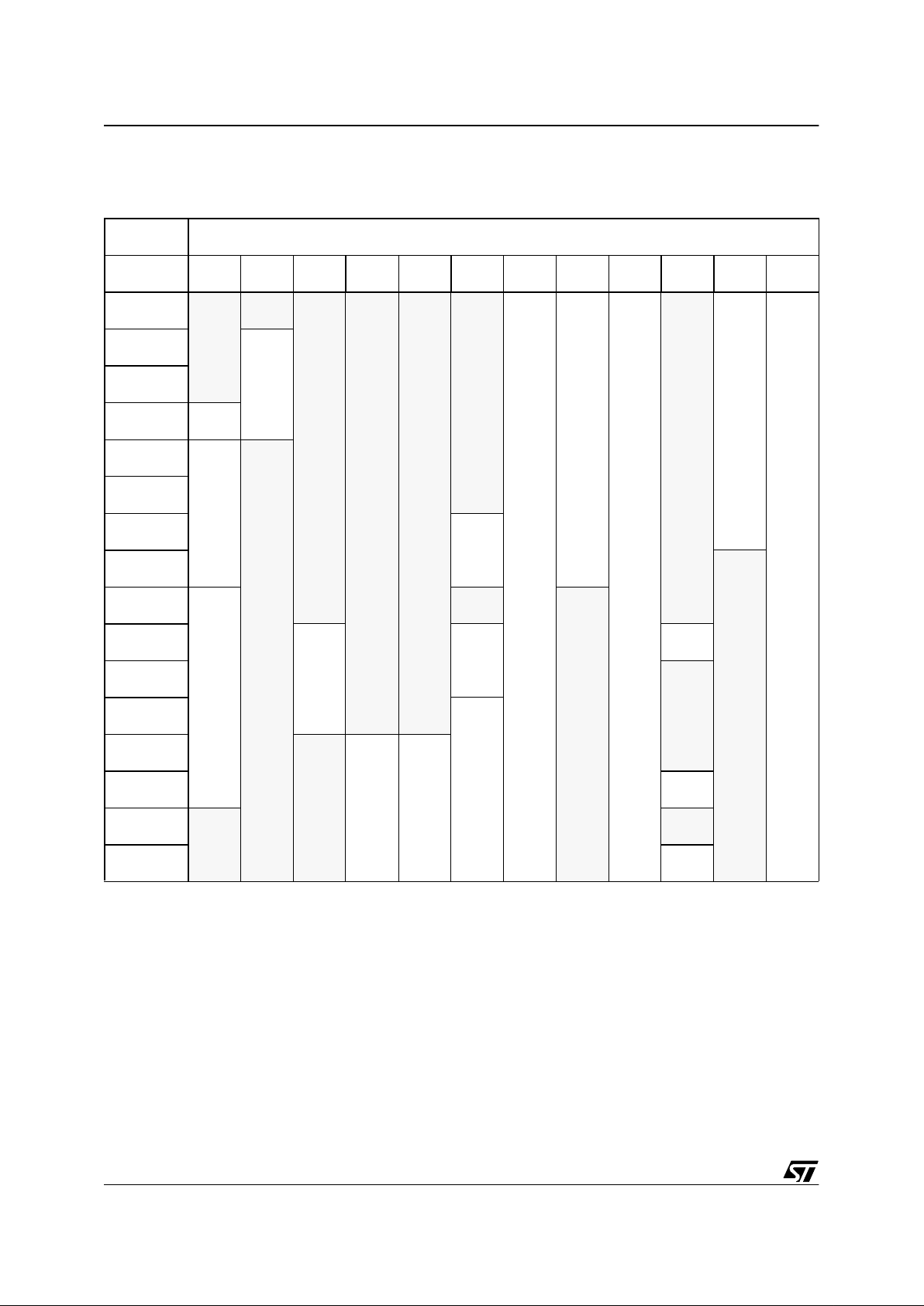
The following pages contain a list of ST92141 registers, grouped by peripheral or function.
Be very careful to correctly program both:
– The set of registers dedicated to a particular
function or peripheral.
– Registers common to other functions.
– In particular, double-check that any registers
with “undefined” reset values have been correct-
ly initial is ed.
WARNING: Note that in the EIVR and each IVR
register, all bits are significant. Take care when
defining base vector ad dresses that en tries in the
Interrupt Vector table do not overlap.
Table 6. Common Registers
Function or Peripheral Common Registers
ADC CICR + NICR + I/O PORT REGISTERS
WDT
CICR + NICR + EXTERNAL INTERRUPT REGISTERS +
I/O PORT REGISTERS
I/O PORTS I/O PORT REGISTERS + MODER
EXTERNAL INTERRUPT INTERRUPT REGISTERS + I/O PORT REGISTERS
RCCU INTERRUPT REGISTERS + MODER
9
16/179
ST92141 - GENER AL DESCRIPTION
Table 7. G roup F Pages
Resources available on the ST92141 devices:
Register Page
0 2 3 7 11 21 28 48 51 55 57 63
R255
Res.
Res.
Res.
Res. Res.
Res.
EFT0
IMC
IMC
Res.
WU
A/D0
R254
PORT
3
R253
R252
WCR
R251
WDT
Res.
R250
R249
MMU
R248
Res.
R247
EXT
INT
Res.
Res.
R246
PORT
5
EM
RCCU
R245
Res.R244
MMU
R243
Res. SPI0 STIM0
R242
RCCU
R241
Res.
Res.
R240
RCCU
9
17/179
ST92141 - GENERAL DESCRIPTION
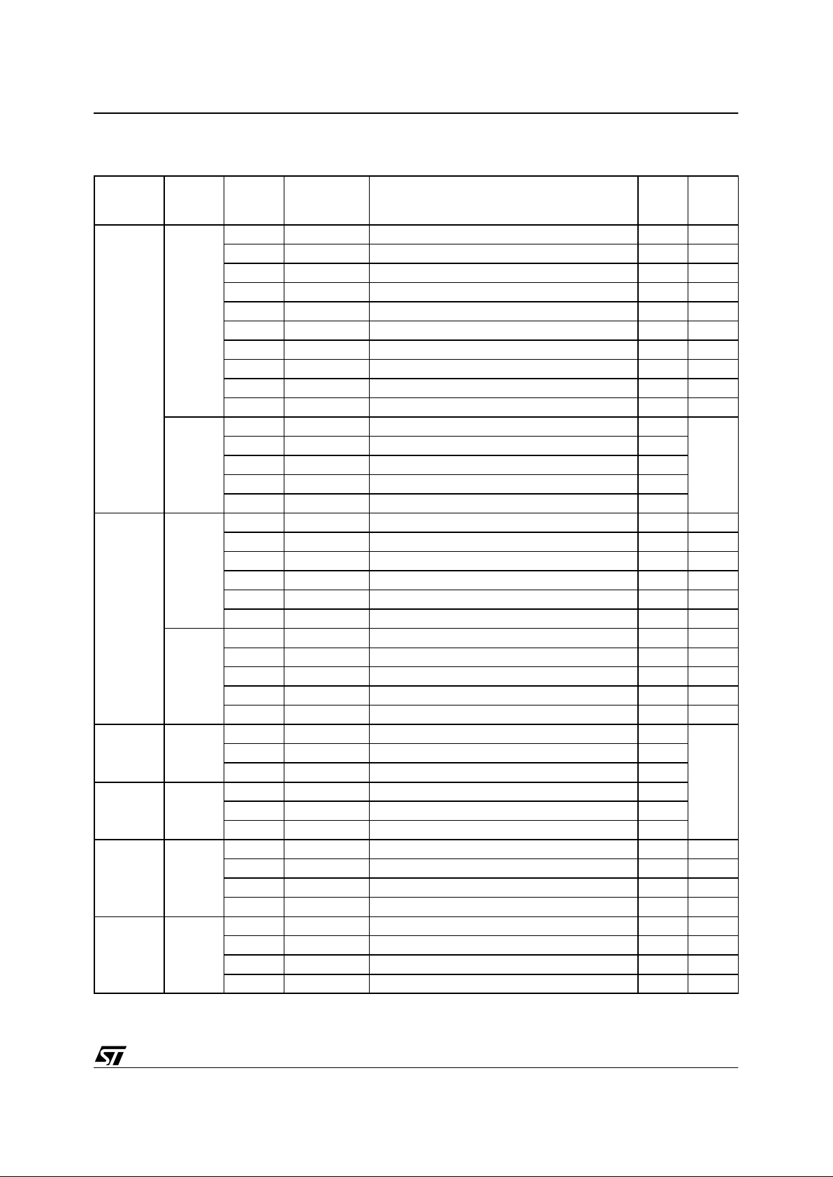
Table 8. Detailed Register Map
Page
(Decimal)
Block
Reg.
No.
Register
Name
Description
Reset
Value
Hex.
Doc.
Page
N/A
Core
R230 CICR Central Interrupt Control Register 87 52
R231 FLAGR Flag Register 00 24
R232 RP0 Pointer 0 Register xx 26
R233 RP1 Pointer 1 Register xx 26
R234 PPR Page Pointer Register xx 28
R235 MODER Mode Register E0 28
R236 USPHR User Stack Pointer High Register xx 30
R237 USPLR User Stack Pointer Low Register xx 30
R238 SSPHR System Stack Pointer High Reg. xx 30
R239 SSPLR System Stack Pointer Low Reg. xx 30
I/O
Port
5:4,2:0
R224 P0DR Port 0 Data Register FF
79
R225 P1DR Port 1 Data Register FF
R226 P2DR Port 2 Data Register FF
R228 P4DR Port 4 Data Register FF
R229 P5DR Port 5 Data Register FF
0
INT
R242 EITR External Interrupt Trigger Regis ter 00 52
R243 EIPR External Interrupt Pending Reg. 00 53
R244 EIMR External Interrupt Mask-bit Reg. 00 53
R245 EIPLR External Interrupt Priority Level Reg. FF 53
R246 EIVR External Interrupt Vector Regis ter x6 54
R247 NICR Nested Interrupt Control 00 54
WDT
R248 WDTHR Watchdog Timer High Register FF 90
R249 WDTLR Watchdog Timer Low Register FF 90
R250 WDTPR Watchdog Timer Prescaler Reg. FF 90
R251 WDTCR Watchdog Timer Control Register 12 90
R252 WCR Wait Control Register 7F 91
2
I/O
Port
3
R252 P3C0 Port 3 Configuration Register 0 00
79
R253 P3C1 Port 3 Configuration Register 1 00
R254 P3C2 Port 3 Configuration Register 2 00
3
I/O
Port
5
R244 P5C0 Port 5 Configuration Register 0 FF
R245 P5C1 Port 5 Configuration Register 1 00
R246 P5C2 Port 5 Configuration Register 2 00
7SPI
R240 SPDR SPI Data Register 00 145
R241 SPCR SPI Control Register 00 145
R242 SPSR SPI Status Register 00 146
R243 SPPR SPI Prescaler Register 00 146
11 STIM
R240 STH Counter High Byte Register FF 95
R241 STL Counter Low Byte Register FF 95
R242 STP Standard Timer Prescaler Register FF 95
R243 STC Standard Timer Control Register 14 95
9
18/179
ST92141 - GENER AL DESCRIPTION
21
MMU
R240 DPR0 Data Page Register 0 xx 35
R241 DPR1 Data Page Register 1 xx 35
R242 DPR2 Data Page Register 2 xx 35
R243 DPR3 Data Page Register 3 xx 35
R244 CSR Code Segment Register 00 36
R248 ISR Interrupt Segment Register xx 36
R249 DMASR DMA Segment Register xx 36
EM
R245 EMR1 EM Register 1 80 62
R246 EMR2 EM Register 2 0F 62
28 EFT
R240 IC1HR Input Capture 1 High Register xx 108
R241 IC1LR Input Capture 1 Low Register xx 108
R242 IC2HR Input Capture 2 High Register xx 108
R243 IC2LR Input Capture 2 Low Register xx 108
R244 C HR Counter High Register FF 109
R245 C LR Counter Low Register FC 109
R246 ACHR Alternate Counter High Register FF 109
R247 ACLR Alternate Counter Low Register FC 109
R248 OC1HR Output Compare 1 High Register 80 110
R249 OC1LR Output Compare 1 Low Register 00 110
R250 OC2HR Output Compare 2 High Register 80 110
R251 OC2LR Output Compare 2 Low Register 00 110
R252 CR1 Control Register 1 00 111
R253 CR2 Control Register 2 00 112
R254 SR Status Register 00 113
R255 CR3 Control Register 3 00 113
48 IMC
R248 PCR0 Peripheral Control Register 0 80 130
R249 PCR1 Peripheral Control Register 1 00 130
R250 PCR2 Peripheral Control Register 2 00 131
R251 PSR Polarity Selection Register 00 131
R252 OPR Output Peripheral Register 00 132
R253 IMR Interrupt Mask Register 00 132
R254 DTG Dead Time Generator Register 00 133
R255 IMCIVR IMC Interrupt Vector Register xx 133
Page
(Decimal)
Block
Reg.
No.
Register
Name
Description
Reset
Value
Hex.
Doc.
Page
9

19/179
ST92141 - GENERAL DESCRIPTION
Note: xx denotes a byte with an undefined value, however some of the bits may have defined values. Refer to register description for details.
51 IMC
R240 TCPTH Tacho Capture Register High xx 125
R241 TCPTL Tacho Capture Register Low xx 125
R242 TCMP Tacho Compare Register xx 125
R243 ISR Interrupt Status Register 3F 36
R244 TPRSH Tacho Prescaler Register High 00 127
R245 TPRSL Tacho Prescaler Register Low 00 127
R246 CPRS PWM Counter Prescaler Register 00 127
R247 REP Repetition Counter Register 00 127
R248 CPWH Compare Phase W Preload Register High 00 128
R249 CPWL Compare Phase W Preload Register Low 00 128
R250 CPVH Compare Phase V Preload Register High 00 128
R251 CPVL Compare Phase V Preload Register Low 00 128
R252 CPUH Compare Phase U Preload Register High 00 129
R253 CPUL Compare Phase U Preload Register Low 00 129
R254 CP0H Compare 0 Preload Register High 00 129
R255 CP0L Compare 0 Preload Register Low 00 129
55 RCCU
R240 CLKCTL Clock Control Register 00 69
R242 CLK_FLAG Clock Flag Register 48, 28 70
R246 PLLCONF PLL Configuration Register xx 71
57 WUIMU
R249 WUCTRL Wake-Up Control Register 00 59
R250 WUMRH Wake-Up Mask Register High 00 60
R251 WUMRL Wake-Up Mask Register Low 00 60
R252 WUTRH Wake-Up Trigger Register High 00 61
R253 WUTRL Wake-Up Trigger Register Low 00 61
R254 WUPRH Wake-Up Pending Register High 00 61
R255 WUPRL Wake-Up Pending Register Low 00 61
63 ADC
R240 D0R Channel 0 Data Register xx 151
R241 D1R Channel 1 Data Register xx 151
R242 D2R Channel 2 Data Register xx 151
R243 D3R Channel 3 Data Register xx 151
R244 D4R Channel 4 Data Register xx 151
R245 D5R Channel 5 Data Register xx 151
R246 D6R Channel 6 Data Register xx 151
R247 D7R Channel 7 Data Register xx 151
R248 LT6R Channel 6 Lower Threshold Reg. xx 152
R249 LT7R Channel 7 Lower Threshold Reg. xx 152
R250 UT6R Channel 6 Upper Threshold Reg. xx 152
R251 UT7R Channel 7 Upper Threshold Reg. xx 152
R252 CRR Compare Result Register 0F 153
R253 CLR Control Logic Register 00 154
R254 ICR Interrupt Control Register 0F 155
R255 IVR Interrupt Vector Register x2 155
Page
(Decimal)
Block
Reg.
No.
Register
Name
Description
Reset
Value
Hex.
Doc.
Page
9

20/179
ST92141 - DEVICE ARCHITECTURE
2 DEVICE ARCHITECTURE
2.1 CORE ARCHITECTURE
The ST9 Core or Central Processing Unit (CPU)
features a highly optimised instruction set, capable
of handling bit, byte (8-bit) and word (16-bit) data,
as well as BCD and Boolean formats; 14 addressing modes are available.
Four independent buses are controlled by the
Core: a 16-bit Memory bus, an 8-bi t Registe r data
bus, an 8-bit Register ad dress bus an d a 6-bit Interrupt/DMA bus which connect s th e in terrupt an d
DMA controllers in the on-chip peripherals with the
Core.
This multiple bus architecture affords a high degree of pipelining and parallel operation, thus making the ST9 family devices highly efficient, both for
numerical calculation, data handling and with regard to communication with on-chip peripheral resources.
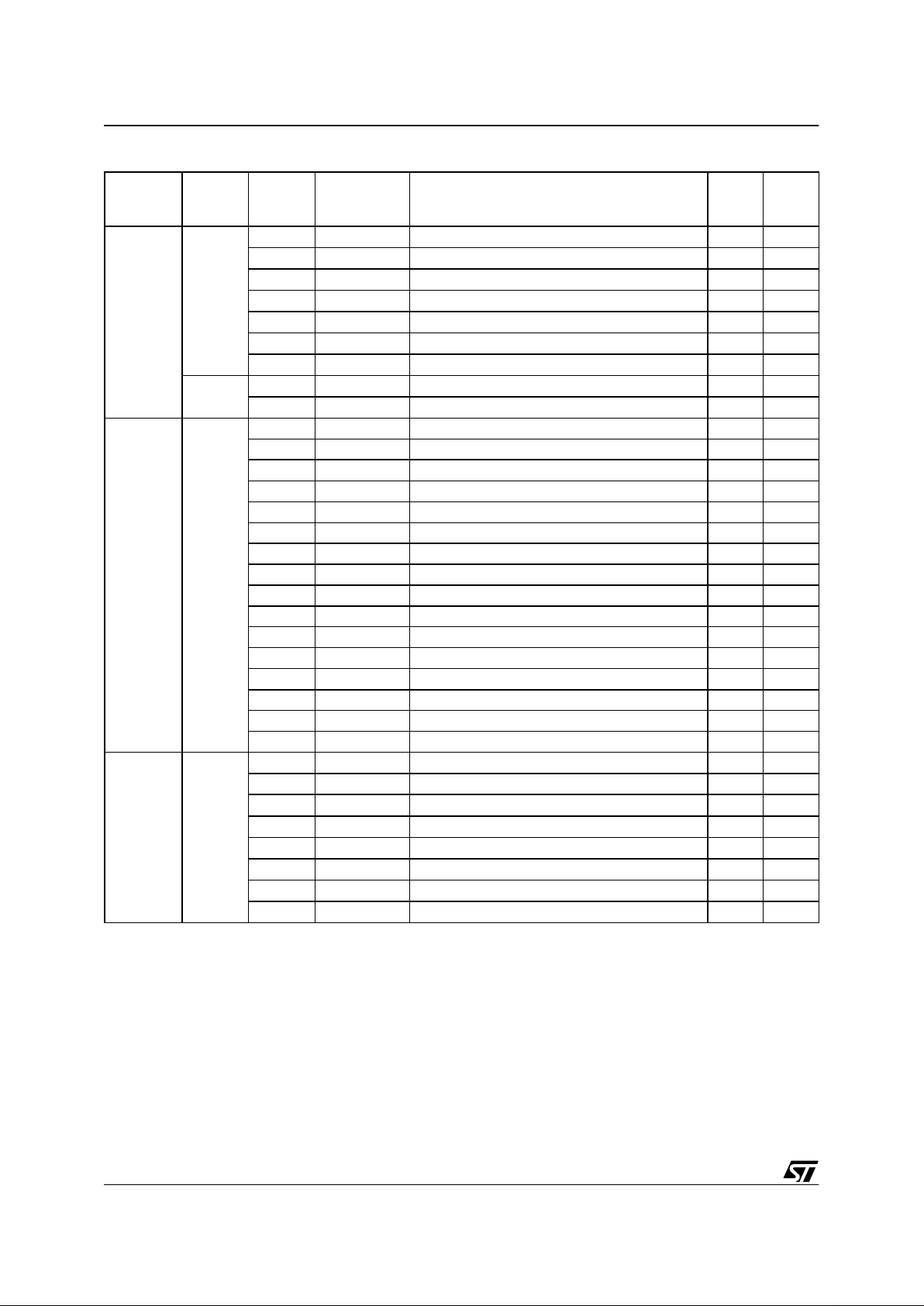
2.2 MEMORY SPACES
There are two separate memory spaces:
– The Register File, which comprises 240 8-bit
registers, arranged as 15 groups (Group 0 to E),
each containing sixteen 8-bit registers plus up to
64 pages of 16 registers mapped in Group F,
which hold data and control bits for the on-chip
peripherals and I/Os.
– A sing le linear memory space acc ommodating
both program and data. All of the physically sep-
arate memory areas, including the internal ROM,
internal RAM and ex ternal memory are mapped
in this common address space. The total ad-
dressable memory space of 4 Mbytes (limited by
the size of on-chip memory and the number of
external address pins) is arranged as 64 seg-
ments of 64 Kbytes. Each segment is further
subdivided into four pages of 16 Kbytes, as illus-
trated in Figure 3. A Memory Man agement Unit
uses a set of pointer registers to address a 22-bit
memory field using 16-bit address-based instruc-
tions.
2.2.1 Reg ister File
The Register File consists of (see Figure 4):
– 224 general purpose registers (Group 0 to D,
registers R0 to R223)
– 6 system registers in the System Group (Group
E, registers R224 to R239)
– Up to 64 pages, depending on device configura-
tion, each containing up to 16 registers, mapped
to Group F (R240 to R255), see Figure 5.
Figure 3. Single Program and Data Memory Address Spac e
3FFFFFh
3F0000h
3EFFFFh
3E0000h
20FFFFh
02FFFFh
020000h
01FFFFh
010000h
00FFFFh
000000h
8
7
6
5
4
3
2
1
0
63
62
2
1
0
Address 16K Pages 64K Segments
up to 4 Mbytes
Data
Code
255
254
253
252
251
250
249
248
247
9
10
11
21FFFFh
210000h
133
134
135
33
Reserved
132
9
21/179
ST92141 - DEVICE ARCHITECTURE
MEMORY SPACES (Cont’d)
Figure 4. Regis te r Gr oups Figure 5. Pag e Pointer for Group F m apping
Figure 6. Addressing the Register File
F
E
D
C
B
A
9
8
7
6
5
4
3
PAGED REGISTERS
SYSTEM REGISTER S
2
1
0
00
15
255
240
239
224
223
VA00432
UP TO
64 PAGES
GENERAL
REGISTERS
PURPOSE
224
PAGE 63
PAGE 5
PAGE 0
PAGE POINT ER
R255
R240
R224
R0
VA00433
R234
REGISTER FILE
SYSTEM REGISTER S
GROU P D
GROUP B
GROUP C
(1100)
(0011)
R192
R207
255
240
239
224
223
F
E
D
C
B
A
9
8
7
6
5
4
3
2
1
0
15
VR000118
00
R195
R195
(R0C3h)
PAGED REGISTERS
9

22/179
ST92141 - DEVICE ARCHITECTURE
MEMORY SPACES (Cont’d)
2.2.2 Register Addressing
Register File registers, including Group F paged
registers (but excluding Group D), may be addressed explicitly by means of a decimal, hexadecimal or binary address; thus R231, RE7h and
R11100111b represent the same register (see
Figure 6). Group D registers can only be ad-
dressed in Working Register mode.
Note that an upper case “R” is used to denote this
direct addressing mode.
Working Re gi st ers
Certain types of instruction require that registers
be specified in the form “rx”, where x is in the
range 0 to 15: these are known as Working Registers.
Note that a lower case “r” is used to denote this indirect addressing mode.
Two addressing schemes are av ailable: a single
group of 16 working registers, or two separately
mapped groups, each consisting of 8 working registers. These groups may be mapped starting at
any 8 or 16 byte boundary in the register file by
means of dedicated pointer registers. This technique is described in more detail in Section 2.3.3
Register Pointing Techniques, and illustrated in
Figure 7 and in Figure 8.
System Registers
The 16 registers in Group E (R224 to R239) are
System registers and may be addressed using any
of the register addressing modes. Thes e registers
are described in greater detail in Section 2.3 SYSTEM REGISTER S.
Paged Registers
Up to 64 pages, each containing 16 registers, may
be mapped to G roup F. These are add ressed using any register addressing mode, in conjunctio n
with the Page Pointer register, R234, which is one
of the System registers. This register selects the
page to be mapped to Group F and, once set,
does not need to be changed if two or more registers on the same page are to be addressed in succession.
Therefore if the Page Pointer, R234, is set to 5, the
instructions:
spp #5
ld R242, r4
will load the contents of working register r4 into the
third register of page 5 (R242).
These paged registers hold data and control information relating to the on-chip peripherals, each
peripheral always being associated with the sam e
pages and registers to ensure code com patibility
between ST9 devices. The number of these registers therefore depends on the peripherals which
are present in the s pecific ST9 family device. In
other words, pages only exist if the relevant peripheral is present.
Table 9. Register File Organization
Hex.
Address
Decimal
Address
Function
Register
File Group
F0-FF 240-255
Paged
Registers
Group F
E0-EF 224-239
System
Registers
Group E
D0-DF 208-223
General
Purpose
Registers
Group D
C0-CF 192-207 Group C
B0-BF 176-191 Group B
A0-AF 160-175 Group A
90-9F 144-159 Group 9
80-8F 128-143 Group 8
70-7F 112-127 Group 7
60-6F 96-111 Group 6
50-5F 80-95 Group 5
40-4F 64-79 Group 4
30-3F 48-63 Group 3
20-2F 32-47 Group 2
10-1F 16-31 Group 1
00-0F 00-15 Group 0
1
23/179
ST92141 - DEVICE ARCHITECTURE
2.3 SYSTEM REGISTERS
The System registers are listed in Table 10 Sy s-
tem Registers (Group E). They are used to per-
form all the important system settings. Their purpose is described in the following pages. Refer t o
the chapter dealing with I/O for a description of the
PORT[5:0] Data registers.
Table 10. System Registers (Group E)
2.3.1 Central Interrupt Control Register
Please refer to the ”INTERRUPT” chapter for a detailed description of the ST9 interrupt philosophy.
CENTRAL INTERRUPT CONTROL REGISTER
(CICR)
R230 - Read/Write
Register Group: E (System)
Reset Value: 1000 0111 (87h)
Bit 7 = GCEN:
Global Counter Enable
.
This bit is the Global Counter Enable of the Multifunction Timers. The GCEN bit is ANDed with the
CE bit in the TCR Register (only in devices featuring the MFT Multifunction Timer) in order to enable
the Timers when both bits are set. This bit is set after the Reset cycle.
Note: If an MFT is not included in the ST9 device,
then this bit has no effect.
Bit 6 = TLIP:
Top Level Interrupt Pending
.
This bit is set by hardware when a Top Level Interrupt Request is recognized. This bit can also be
set by software to simulate a Top Level Interrupt
Request.
0: No Top Level Interrupt pending
1: Top Level Interrupt pending
Bit 5 = TLI:
Top Level Interrupt bit
.
0: Top Level Interrupt is acknowledged depending
on the TLNM bit in the NICR Register.
1: Top Level Interrupt is acknowledged depending
on the IEN and TLNM bits in the NICR Register
(described in the Interrupt chapter).
Bit 4 = IEN:
Interrupt Enable .
This bit is cleared by interrupt acknowledgement,
and set by interrupt return (iret). IEN is modified
implicitl y by iret, ei and di instructions or by an
interrupt acknowledge cycle. It can also be explicitly written by the user, but only when no i nterrupt
is pending. Therefore, the user should execute a
di instruction (or guarantee by other means that
no interrupt request can arrive) before a ny write
operation to the CICR register.
0: Disable all interrupts except Top Level Interrupt.
1: Enable Interrupts
Bit 3 = IAM:
Interrupt Arbitration Mode
.
This bit is set and cleared by software to select the
arbitration mode.
0: Concurrent Mode
1: Nested Mode.
Bits 2:0 = CPL[2:0]:
Current Priority Level
.
These three bits record the priority level of the routine currently running (i.e. the Current Priority Level, CPL). The highest priority level is represented
by 000, and the lowest by 111. The CPL bits can
be set by hardware or software and provide the
reference according to which subsequent interrupts are either left pending or are allowed to interrupt the current interrupt service routine. When the
current interrupt is replaced by one of a higher priority, the current priority value is automatically
stored until required in the NICR register.
R239 (EFh) SSPLR
R238 (EEh)
SSPHR
R237 (EDh)
USPLR
R236 (ECh)
USPHR
R235 (EBh)
MODE REGISTER
R234 (EAh)
PAGE POINTER REGISTER
R233 (E9h)
REGISTER POINTER 1
R232 (E8h)
REGISTER POINTER 0
R231 (E7h)
FLAG REGISTER
R230 (E6h)
CENTRAL INT. CNTL REG
R229 (E5h)
PORT5 DATA REG.
R228 (E4h)
PORT4 DATA REG.
R227 (E3h)
PORT3 DATA REG.
R226 (E2h)
PORT2 DATA REG.
R225 (E1h)
PORT1 DATA REG.
R224 (E0h)
PORT0 DATA REG.
70
GCEN TLIP TLI IEN IAM CPL2 CPL1 CPL0
1

24/179
ST92141 - DEVICE ARCHITECTURE
SYSTEM REGI STE R S (Cont’d)
2.3.2 Flag Register
The Flag Register contains 8 flags which indicate
the CPU status. During an interrupt, the flag register is automatically stored in the system stack area
and recalled at the end of the interrupt service routine, thus returning the CPU to its original status.
This occurs for all interrupts and, wh en operating
in nested mode, up to seven versions of the flag
register may be stored.
FLAG REGISTER (FLAGR)
R231- Read/Write
Register Group: E (System)
Reset value: 0000 0000 (00h)
Bit 7 = C :
Carry Flag
.
The carry flag is affected by:
Addition (add, addw, adc, adcw),
Subtraction (sub, subw, sbc, sbcw),
Compare (cp, cpw),
Shift Right Arithmetic (sra, sraw),
Shift Left A r ith me t ic (sla, slaw),
Swap Nibbles (swap),
Rotate (rrc, rrcw, rlc, rlcw, ror,
rol),
Decimal Adjust (da),
Multiply and Divide (mul, div, divws).
When set, it generally indicates a carry out of the
most significant bit position of the register being
used as an accumulator (bit 7 for byte operations
and bit 15 for word operations).
The carry flag can be set by the S et Carry Flag
(scf ) instruction, cleared by the Reset Carry Flag
(rcf) instruction, and complemented by the Complement Carry Flag (ccf) instruction.
Bit 6 = Z:
Zero Flag
. The Zero flag is affected by:
Addition (add, addw, adc, adcw),
Subtraction (sub, subw, sbc, sbcw),
Compare (cp, cpw),
Shift Right Arithmetic (sra, sraw),
Shift Left A r ith me t ic (sla, slaw),
Swap Nibbles (swap),
Rotate (rrc, rrcw, rlc, rlcw, ror,
rol),
Decimal Adjust (da),
Multiply and Divide (mul, div, divws),
Logical (and, andw, or, orw, xor,
xorw, cpl),
Increment and Decrement (inc, incw, dec,
decw),
Test (tm, tmw, tcm, tcmw, btset).
In most cases, the Zero flag is set when the contents
of the register being used as an accumulator become zero, following one of the above operations.
Bit 5 = S:
Sign Flag
.
The Sign flag is affected by the same instructions
as the Zero flag.
The Sign flag is set when bit 7 (for a byte operation) or bit 15 (for a word operation) of the register
used as an accumulator is one.
Bit 4 = V:
Overflow Flag
.
The Overflow flag is affected by t he sa me instructions as the Zero and Sign flags.
When set, the Overflow flag indicates that a two'scomplement number, in a result register, is in error, since it has exceeded the largest (or is less
than the smallest), number that can be represented in two’s-complement notation.
Bit 3 = DA:
Decimal Adjust Flag
.
The DA flag is used f or BCD arithm et ic. Si nce t he
algorithm for correcting BCD operations i s different for addition and subtraction, this flag is used to
specify which type of instruction was executed
last, so that the subsequen t Decimal Adjust (da)
operation can perform its function correctly. The
DA flag cannot normally be u sed as a test condition by the programmer.
Bit 2 = H:
Half Carry Flag.
The H flag indicates a carry out of (or a borrow into) bit 3, as the resu lt of addin g or subt racti ng tw o
8-bit bytes, each representing two BCD digits. The
H flag is used by the Dec imal Adjust (da) instruc-
tion to convert the binary result of a previous addition or subtraction into the correct BCD result. Like
the DA flag, this flag is not norma lly accessed by
the user.
Bit 1 = Reserved bit (must be 0).
Bit 0 = DP:
Data/Program Memory Flag
.
This bit indicates the memory area addressed . Its
value is affected by the Set Data Memory (sdm)
and Set Program Mem ory (spm) instructions. Refer to the Memory Management Unit for further details.
70
C Z S V DA H - DP
1

25/179
ST92141 - DEVICE ARCHITECTURE
SYSTEM REGI STE R S (Cont’d)
If the bit is set, dat a is accessed using the Data
Pointers (DPRs registers), otherwise it is pointed
to by the Code Pointer (CSR regist er); therefore,
the user initialization routine must include a Sdm
instruction. Note that code is always poi nted to by
the Code Pointer (CSR).
Note: In the current ST9 devices, the DP flag is
only for co mpatibility wit h software d eveloped for
the first generation of ST9 devices. With the single
memory addressing space, its us e is now redundant. It must be kept to 1 w ith a Sdm instruction at
the beginning of the program to ens ure a normal
use of the different memory pointers.
2.3.3 Register Pointing Techniques
Two registers within the System register group,
are used as pointers to the working registers. Register Pointer 0 (R232) may be used on its own as a
single pointer to a 16-register working space, or in
conjunction with Register Pointer 1 (R233), to
point to two separate 8-register spaces.
For the purpose of register pointing, the 16 register
groups of the register file are subdivided into 32 8register blocks. The values specified with the Set
Register Pointer instructions refer to the blocks to
be pointed to in twin 8-register mode, or to the lower 8-register block location in single 16-register
mode.
The Set Registe r Pointer instructions srp, srp0
and srp1 automatically inform the C PU whether
the Register File is to operate in single 16-register
mode or in twin 8-register mode. The srp instruction selects the single 16-register group mode and
specifies the location of the lower 8-register block,
while the srp0 and srp1 instructions automatically select the twin 8-register group mode and specify the locations of each 8-register block.
There is no limitation on the order or position of
these register groups, other than that they must
start on an 8-register boundary i n twin 8-register
mode, or on a 16-register boundary in single 16register mode.
The block number should always be an even
number in single 16-re gister mode. The 16-register group will always start at the block whose
number is the nearest even number equal to or
lower than the block number specified in the srp
instruction. Avoid using odd block numbers , since
this can be confusing if twin mode is subsequently
selected.
Thus:
srp #3 will be interpreted as srp #2 and will al-
low using R16 ..R31 as r0 .. r15.
In single 16-register mode , the working registers
are referred to as r0 to r15. In twin 8-register
mode, registers r0 to r7 are in the block pointed
to by RP0 (by means of the srp0 instruction),
while registers r8 to r15 are in the block pointed
to by RP1 (by means of the srp1 instructio n).
Caution:
Group D registers can only be accessed
as working registers using the Register Pointers,
or by means of the Stack Pointers. They cannot be
addressed explicitly in the form “Rxxx”.
1

26/179
ST92141 - DEVICE ARCHITECTURE
SYSTEM REGI STE R S (Cont’d)
POINTER 0 REGIST ER (RP0)
R232 - Read/Write
Register Group: E (System)
Reset Value: xxxx xx00 (xxh)
Bits 7:3 = RG[4:0]:
Register Group number.
These bits contain the num ber (in the range 0 to
31) of the register block s pecified in the srp0 or
srp instructions. In single 16-register mode the
number indicates the lower of the two 8-register
blocks to which the 16 working registers are to be
mapped, while in twin 8-register mode it indicates
the 8-register block to which r0 to r7 are to be
mapped.
Bit 2 = RPS:
Register Pointer Selector
.
This bit is set by the instructions srp0 and srp1 to
indicate that the twin register po inting m ode is s elected. The bit is reset by the srp instruction to indicate that the single register pointing mode is selected.
0: Single register pointing mode
1: Twin register pointing mode
Bits 1:0: Reserved. Forced by hardware to zero.
POINTER 1 REGISTER (RP1)
R233 - Read/Write
Register Group: E (System)
Reset Value: xxxx xx00 (xxh)
This register is only used in the twin register pointing mode. W hen us ing t he sin gle regist er pointing
mode, or when using only one of the twin regi ster
groups, the RP1 register must be considered as
RESERVED and may NOT be us ed as a general
purpose register.
Bits 7:3 = RG[4:0]:
Register Group number.
These bits contain the n umber (in the range 0 to
31) of the 8-register block specified in the srp1 instruction, to which r8 to r15 are to be mapped.
Bit 2 = RPS:
Register Pointer Selector
.
This bit is set by the srp0 and srp1 instructions to
indicate that the twin registe r pointing mod e is s elected. The bit is reset by the srp instruction to indicate that the single register pointing mode i s selected.
0: Single register pointing mode
1: Twin register pointing mode
Bits 1:0: Reserved. Forced by hardware to zero.
70
RG4 RG3 RG2 RG1 RG0 RPS 0 0
70
RG4 RG3 RG2 RG1 RG0 RPS 0 0
1

27/179
ST92141 - DEVICE ARCHITECTURE
SYSTEM REGI STE R S (Cont’d)
Figure 7. Pointing to a single group of 16
registers
Figure 8. Pointing to two groups of 8 registers
31
30
29
28
27
26
25
9
8
7
6
5
4
3
2
1
0
F
E
D
4
3
2
1
0
BLOCK
NUMBER
REGISTER
GROUP
REGISTER
FILE
REGISTER
POINTER 0
srp #2
set by:
instruction
points to:
GROUP 1
addressed by
BLOCK 2
r15
r0
31
30
29
28
27
26
25
9
8
7
6
5
4
3
2
1
0
F
E
D
4
3
2
1
0
BLOCK
NUMBER
REGISTER
GROUP
REGISTER
FILE
REGISTER
POINTER 0
srp0 #2
set by:
instructions
point to:
GROUP 1
addressed by
BLOCK 2
&
REGISTER
POINTER 1
srp1 #7
&
GROUP 3
addressed by
BLOCK 7
r7
r0
r15
r8
1
28/179
ST92141 - DEVICE ARCHITECTURE
SYSTEM REGI STE R S (Cont’d)
2.3.4 Paged Registers
Up to 64 pages, each containing 16 registers, may
be mapped to Group F. These paged registers
hold data and control information relating to the
on-chip peripherals, each peripheral a lways being
associated with the same pages and registers to
ensure code compa tibility bet ween ST9 devices.
The number of these registers depends on the peripherals present in the specific ST9 device. In other words, pages only exist if the relevant peripheral is present.
The paged registers are addressed using the normal register addressing modes, in conjunction with
the Page Pointer register, R234, which is on e of
the System registers. This register selects the
page to be mapped to Group F and, once set,
does not need to be changed if two or more registers on the same page are to be addressed in succession.
Thus the instructions:
spp #5
ld R242, r4
will load the contents of working register r4 into the
third register of page 5 (R242).
Warning: During an interrupt, the PPR register is
not saved automatically in the stack. If needed, it
should be saved/restored by the user within the interrupt routine.
PAGE POINTER REGIST ER ( PPR)
R234 - Read/Write
Register Group: E (System)
Reset value: xxxx xx00 (xxh)
Bits 7:2 = PP[5:0]:
Page Pointer
.
These bits contain the num ber (in the range 0 to
63) of the page specified in the spp instruction.
Once the page pointer has been set , there is no
need to refresh it unless a different page is required.
Bits 1:0: Reserved. Forced by hardware to 0.
2.3.5 Mode Regi ster
The Mode Register allows control of the following
operating parameters:
– Selection of internal or external System and User
Stack areas,
– Management of the clock frequency,
– Enabl ing of Bus request and Wait s ignals when
interfacing to external memory.
MODE REGISTER (MODER)
R235 - Read/Write
Register Group: E (System)
Reset value: 1110 0000 (E0h)
Bit 7 = SSP:
System Stack Point er
.
This bit selects an internal or external System
Stack area.
0: External system stack area, in memory space.
1: Internal system stack area, in the Register File
(reset state).
Bit 6 = USP:
User Stack Pointer
.
This bit selects an internal or external User S tack
area.
0: External user stack area, in memory space.
1: Internal user stack area, in the Register File (re-
set state).
Bit 5 = DIV2:
Crystal Oscillator Clock Divided by 2
.
This bit controls the divide-by-2 circuit operating
on the crystal oscillator clock (CLOCK1).
0: Clock divided by 1
1: Clock divided by 2
Bits 4:2 = PRS[2:0]:
CPUCLK Prescaler
.
These bits load the prescaler division factor for the
internal clock (INTCLK). The prescaler factor selects the internal clock frequency, which can be divided by a factor from 1 to 8. Refer to the Re set
and Clock Control chapter for further information.
Bit 1 = BRQEN:
Bus Request Enable
.
0: External Memory Bus Request disabled
1: External Memory Bus Request enabled on
BREQ
pin (where available).
Note: Disregard this bit if BREQ
pin is not availa-
ble.
Bit 0 = HIMP:
High Impedance Enable
.
When any of Po rts 0, 1, 2 or 6 d epending on device configuration, are programmed as Address
and Data lines to interface external Memory, these
lines and the Memory interface control lines (AS,
DS, R/W) can be forced into the High Impedance
70
PP5 PP 4 PP3 PP2 PP1 P P0 0 0
70
SSP USP DIV2 PRS2 PRS1 PRS0 BRQEN HIMP
1

29/179
ST92141 - DEVICE ARCHITECTURE
SYSTEM REGI STE R S (Cont’d)
state by setting the HIMP bit. When this bit is reset,
it has no effect.
Setting the HIMP bit is recommended for noise reduction when only internal Memory is used.
If Port 1 and/or 2 are declared as an address AND
as an I/O port (for example: P10... P14 = Address,
and P15... P17 = I/O), the HIMP b it has no effect
on the I/O lines.
2.3.6 Stack Pointers
Two separate, double-register stack pointers are
available: the System Stack Pointer and the User
Stack Pointer, both of which can address registers
or memor y .
The stack pointers point to the “bottom” of the
stacks which are filled us ing the pus h comma nds
and emptied using the pop command s. The stack
pointer is automatically pre-decremented when
data is “pushed” in and post-incremented when
data is “popped” out.
The push and pop commands used to manage the
System Stack may be addressed to the User
Stack by adding the suffix “u”. To use a stack in-
struction for a word, the suffix “w” is added. These
suffixes may be combined.
When bytes (or words) are “popped” out from a
stack, the contents of the stack locat ions are unchanged until fresh data is loaded. Thus, when
data is “popped” from a stack area, the stack contents remain unchanged.
Note: Instructions such as: pushuw RR236 or
pushw RR238, as well as the corresponding
pop instructions (where R236 & R237, and R238
& R239 are themselves the user and system stack
pointers respectively), must not be used, since the
pointer values are themselves automatically
changed by the push or pop instruction, thus corrupting their value.
System Stack
The System Stack is us ed for the temporary storage of system and/or control data, such as the
Flag register and the Program counter.
The following automatically push data onto the
System Stack:
– Interrupts
When entering an interrupt, the PC and the Flag
Register are pushed onto the System Stack. If the
ENCSR bit in the EMR2 register is set, then the
Code Segment Re gister is also pushed onto the
System Stack.
– Subroutine Cal ls
When a call instruction is executed, only the PC
is pushed onto stack, where as when a calls instruction (call segment) is executed, both the PC
and the Code Se gment Regist er are pushed ont o
the System Stack.
– Link Instruction
The link or linku instructions create a C lan-
guage stack frame of user-defined length in the
System or User Stack.
All of the above conditions are associated with
their counterparts, such as return instructions,
which pop the stored data items off the stack.
User Stack
The User Stack provides a totally user-co ntrolled
stacking area .
The User Stack Pointer consists of tw o registers,
R236 and R237, which are both used for addressing a stack in memory. When stacking in the Register File, the User Stack Pointer High Register,
R236, becomes redundant but must be considered as reserved.
Stack Pointers
Both System and User stacks are pointed to by
double-byte stack pointers. Stacks m ay be set up
in RAM or in the Register File. Only the lower byte
will be required if the stack is in t he Register File.
The upper byte must then be considered as reserved and must not be used as a general purpose
register.
The stack pointer registers are located in the S ystem Group of the Register File, this is illustrated in
Table 10 System Registers (Group E).
Stack Location
Care is necessary when managing stacks as there
is no limit to stack sizes apart from t he bottom of
any address space in which the stack is placed.
Consequently programmers are advised to use a
stack pointer value as high as possible, particularly when using the Register File as a stacking area.
Group D is a good location for a stack in the Register File, since it is the highest available area. The
stacks may be located anywhere in the first 14
groups of the Register File (internal stacks) or in
RAM (external stacks).
Note. Stacks must not be located in the Paged
Register Group or in the System Register Group.
1
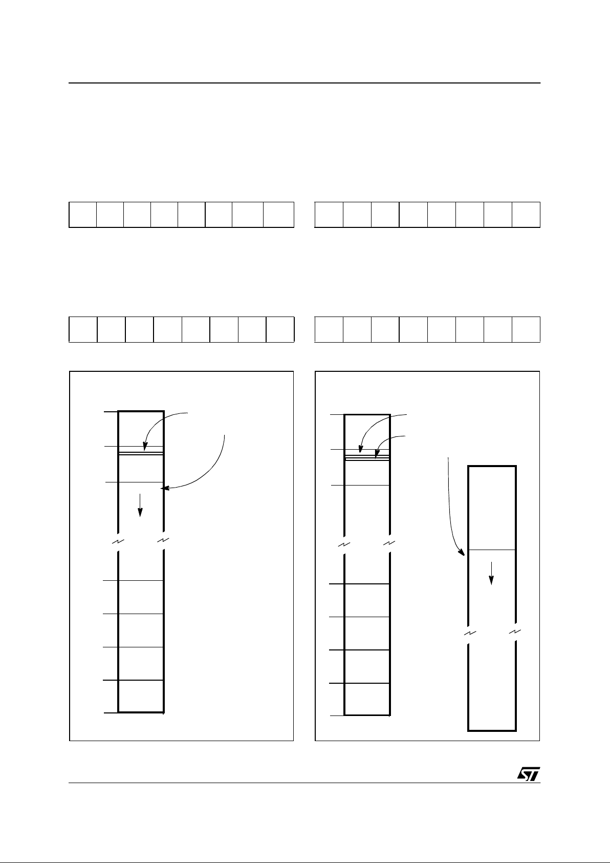
30/179
ST92141 - DEVICE ARCHITECTURE
SYSTEM REGI STE R S (Cont’d)
USER STACK POINTER HIGH REGISTER
(USPHR)
R236 - Read/Write
Register Group: E (System)
Reset value: undefined
USER STACK POINTER LOW REGISTER
(USPLR)
R237 - Read/Write
Register Group: E (System)
Reset value: undefined
Figure 9. Internal Stack Mode
SYSTEM STACK POINTER HIGH REGISTER
(SSPHR)
R238 - Read/Write
Register Group: E (System)
Reset value: undefined
SYSTEM STACK POINTER LOW REGISTER
(SSPLR)
R239 - Read/Write
Register Group: E (System)
Reset value: undefined
Figure 10. External Stack Mode
70
USP15 USP14 USP13 USP12 USP11 USP10 USP9 USP8
70
USP7 USP6 USP5 USP4 USP3 USP2 USP1 USP0
F
E
D
4
3
2
1
0
REGISTER
FILE
STACK POINTER (LOW)
points to:
STACK
70
SSP15 SSP14 SSP13 SSP12 SSP11 SSP10 SSP9 SSP8
70
SSP7 SSP6 SSP5 SSP4 SSP3 SSP2 SSP1 SSP0
F
E
D
4
3
2
1
0
REGISTER
FILE
STACK POINTER (LOW)
point to:
STACK
MEMORY
STACK POINTER (HIGH)
&
1
 Loading...