

SGS Thomson Microelectronics ST92F150, ST92F150CR1, ST92F124R9, ST92F124, ST92F250CV2 Datasheet
...
December 2002 1/398
This is preliminary information on a new product now in development or undergoing evaluation. Details are subject to change without not ice .
Rev. 1.3
ST92F124/ST92F150/ST92F250
8/16-BIT SINGLE VOLTAGE FLASH MCU FAMILY WITH RAM,
E
3 TM
(EMULATED EEPROM), CAN 2.0B AND J1850 BLPD
PRELIMINARY DATA
■ Memories
– Internal Memory : Single Voltage FLASH up to 256
Kbytes, RAM up to 8Kbytes, 1K byte E
3 TM
(Emulat-
ed EEPROM)
– In-Application Programming (IAP)
– 224 general purpose re gisters (regist er file) ava ila-
ble as RAM, accumulators or index pointers
■ Clock, Re set and Supply M a nagement
– Register-oriented 8/16 bit CORE with RUN, WFI,
SLOW, HALT and STOP modes
– 0-24 MHz Operation (Int. Clock), 4.5-5.5 V range
– PLL Clock Generator (3-5 MHz crystal)
– Minimum instruction time: 83 ns (24 MHz int. clock)
■ 80, 77 or 48 I/O pins (depending on device)
■ Interrupt Management
– 80, 77 or 48 I/O pins (depending on device)
– 4 external fast interrupts + 1 NMI
– Up to 16 pins programmable as wake-up or addition-
al external interrupt with multi-level interrupt handler
– DMA controller for reduced processor overhead
■ Timers
– 16-bit Timer with 8-bit Prescaler, and Watchdog Tim-
er (activated by software or by hardware)
– 16-bit Standar d Tim er th at ca n be used to genera te
a time base independent of PLL Clock Generator
– Two 16-bit indepe ndent Extended Functio n Timers
(EFTs) with Prescaler, 2 Input Captures and two
Output Compares (100-pin devices only)
– Two 16-bit Multifunction Timers, with Prescaler, 2 In-
put Captures and two Output Compares
■ Communication Interfaces
– Serial Peripheral Interface (SPI) with Selectable
Master/Slave mode
– One Multiprotocol Serial Com munications Interface
with asynchronous and synchronous capabilities
– One asynchronous Serial Communications Interface
(on 100-pin versions only) with 13-bit LIN Synch
Break generation capability
– J1850 Byte Level Protocol Decoder (JBLPD)
(on F150J versions only)
– One or two full I²C mu ltiple Maste r/Slave Inte rfaces
supporting Access Bus
– One or two CAN 2.0B (150 version only) Active inter-
faces
■ 10-bit Analog to Digital Converter allowing up to 16
input channels on 100-pin devices or 8 input channels
on 64-pin devices
■ Development Tools
– Free High performance Development environment
(IDE) based on Visual Debugger, Assembler, Linker,
and C-Comp iler; Real Tim e Ope rating Syste m (OS EK OS, CMX) and CAN drivers
– Hardware Emula tor and Flash Pro gramming Board
for development and ISP Flasher for production
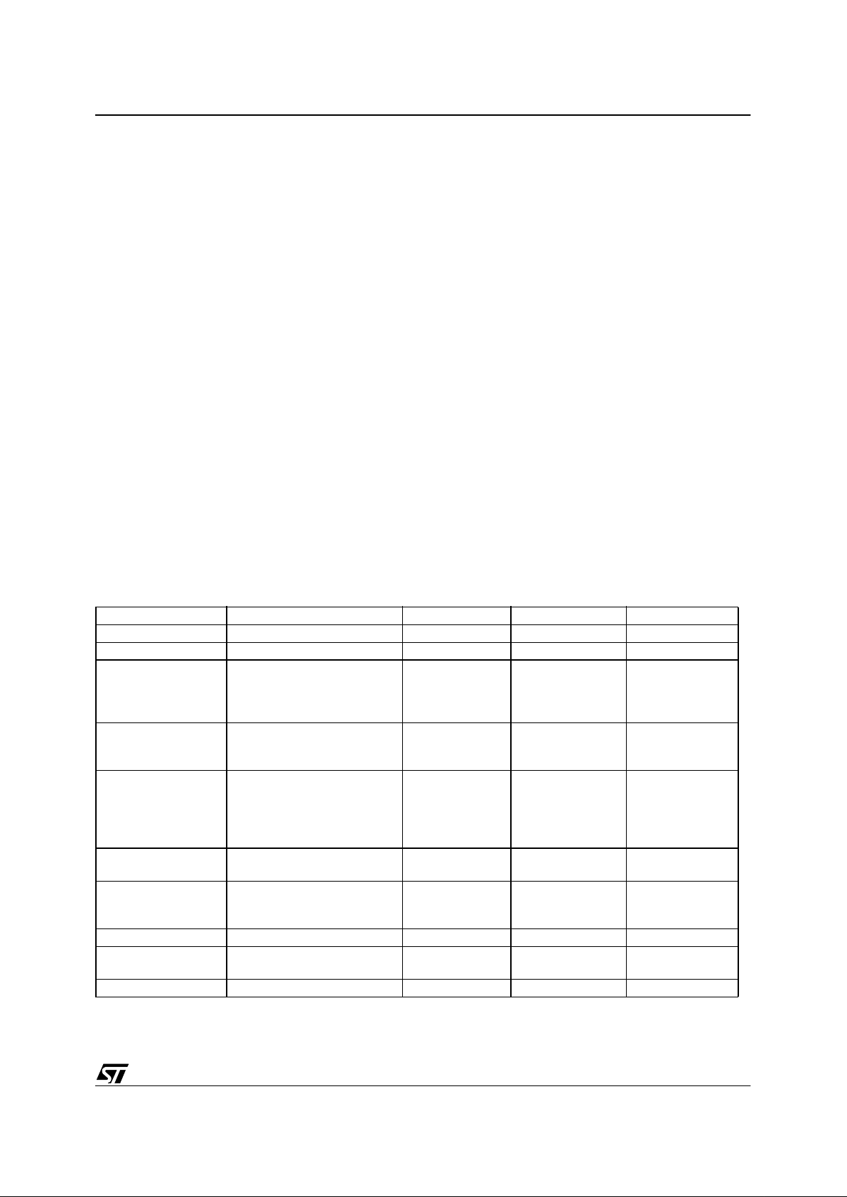
DEVICE SUMMARY
1) see Section 12.3 on page 396 for important information
2) see Table 70 on page 393
PQFP100
14x20
TQFP64
14x14
TQFP100
14x14
Features ST92F124R9 ST92F124V1 ST92F150C(R/V)1 ST92F150JDV1 ST92F250CV2
FLASH - bytes 64K 128K 128K 128K 256K
RAM - bytes 2K 4K 4K 6K 8K
E
3 TM
- bytes 1K 1K 1K 1K 1K
Timers and Serial
Interface
2 MFT, STIM,
WD, SCI, SPI,
I²C
2 MFT, 2 EFT,
STIM, WD,
2 SCI, SPI, I²C
2 MFT, 0/2 EFT,
STIM, WD,
1/2 SCI, SPI, I²C
2 MFT, 2 EFT,
STIM, WD,
2 SCI, SPI, I²C
2 MFT, 2 EFT, STIM,
WD, 2 SCI,
SPI, 2 I²C
1)
ADC 8 x 10 bits 16 x 10 bits 8/16 x 10 bits 16 x 10 bits
Network Interface - CAN 2 CAN, J1850 CAN, LIN Master
Temp. Range -40°C to 85°C -40°C to 105°C
-40°C to 105°C ,
-40°C to 125°C
2)
-40oC to 125oC
-40°C to 105°C ,
-40°C to 125°C
2)
Packages TQFP64 PQFP100
P/TQFP100 and
TQFP64
P/TQFP100
9

2/398
Table of Contents
398
9
1 GENERAL DESCRIPTION . . . . . . . . . . . . . . . . . . . . . . . . . . . . . . . . . . . . . . . . . . . . . . . . . . . . . . 4
1.1 INTRODUCTION . . . . . . . . . . . . . . . . . . . . . . . . . . . . . . . . . . . . . . . . . . . . . . . . . . . . . . . . 4
1.2 PIN DESCRIPTION . . . . . . . . . . . . . . . . . . . . . . . . . . . . . . . . . . . . . . . . . . . . . . . . . . . . . 10
1.3 VOLTAGE REGULATOR . . . . . . . . . . . . . . . . . . . . . . . . . . . . . . . . . . . . . . . . . . . . . . . . 22
1.4 I/O PORTS . . . . . . . . . . . . . . . . . . . . . . . . . . . . . . . . . . . . . . . . . . . . . . . . . . . . . . . . . . . . 23
1.5 ALTERNATE FUNCTIONS FOR I/O PORTS . . . . . . . . . . . . . . . . . . . . . . . . . . . . . . . . . 25
1.6 OPERATING MODES . . . . . . . . . . . . . . . . . . . . . . . . . . . . . . . . . . . . . . . . . . . . . . . . . . . 29
2 DEVICE ARCHITECTURE . . . . . . . . . . . . . . . . . . . . . . . . . . . . . . . . . . . . . . . . . . . . . . . . . . . . . 30
2.1 CORE ARCHITECTURE . . . . . . . . . . . . . . . . . . . . . . . . . . . . . . . . . . . . . . . . . . . . . . . . . 30
2.2 MEMORY SPACES . . . . . . . . . . . . . . . . . . . . . . . . . . . . . . . . . . . . . . . . . . . . . . . . . . . . . 30
2.3 SYSTEM REGISTERS . . . . . . . . . . . . . . . . . . . . . . . . . . . . . . . . . . . . . . . . . . . . . . . . . . 33
2.4 MEMORY ORGANIZATION . . . . . . . . . . . . . . . . . . . . . . . . . . . . . . . . . . . . . . . . . . . . . . 41
2.5 MEMORY MANAGEMENT UNIT . . . . . . . . . . . . . . . . . . . . . . . . . . . . . . . . . . . . . . . . . . 42
2.6 ADDRESS SPACE EXTENSION . . . . . . . . . . . . . . . . . . . . . . . . . . . . . . . . . . . . . . . . . . 43
2.7 MMU REGISTERS . . . . . . . . . . . . . . . . . . . . . . . . . . . . . . . . . . . . . . . . . . . . . . . . . . . . . 44
2.8 MMU USAGE . . . . . . . . . . . . . . . . . . . . . . . . . . . . . . . . . . . . . . . . . . . . . . . . . . . . . . . . . . 48
3 SINGLE VOLTAGE FLASH & E3 TM (EMULATED EEPROM) . . . . . . . . . . . . . . . . . . . . . . . . . 49
3.1 INTRODUCTION . . . . . . . . . . . . . . . . . . . . . . . . . . . . . . . . . . . . . . . . . . . . . . . . . . . . . . . 49
3.2 FUNCTIONAL DESCRIPTION . . . . . . . . . . . . . . . . . . . . . . . . . . . . . . . . . . . . . . . . . . . . 51
3.3 REGISTER DESCRIPTION . . . . . . . . . . . . . . . . . . . . . . . . . . . . . . . . . . . . . . . . . . . . . . . 55
3.4 WRITE OPERATION EXAMPLE . . . . . . . . . . . . . . . . . . . . . . . . . . . . . . . . . . . . . . . . . . . 59
3.5 PROTECTION STRATEGY . . . . . . . . . . . . . . . . . . . . . . . . . . . . . . . . . . . . . . . . . . . . . . . 60
3.6 FLASH IN-SYSTEM PROGRAMMING . . . . . . . . . . . . . . . . . . . . . . . . . . . . . . . . . . . . . . 63
4 REGISTER AND MEMORY MAP . . . . . . . . . . . . . . . . . . . . . . . . . . . . . . . . . . . . . . . . . . . . . . . . 65
4.1 INTRODUCTION . . . . . . . . . . . . . . . . . . . . . . . . . . . . . . . . . . . . . . . . . . . . . . . . . . . . . . . 65
4.2 MEMORY CONFIGURATION . . . . . . . . . . . . . . . . . . . . . . . . . . . . . . . . . . . . . . . . . . . . . 65
4.3 ST92F124/F15 0/F250 RE GI STE R MAP . . . . . . . . . . . . . . . . . . . . . . . . . . . . . . . . . . . . . 70
5 INTERRUPTS . . . . . . . . . . . . . . . . . . . . . . . . . . . . . . . . . . . . . . . . . . . . . . . . . . . . . . . . . . . . . . . 88
5.1 INTRODUCTION . . . . . . . . . . . . . . . . . . . . . . . . . . . . . . . . . . . . . . . . . . . . . . . . . . . . . . . 88
5.2 INTERRUPT VECTORING . . . . . . . . . . . . . . . . . . . . . . . . . . . . . . . . . . . . . . . . . . . . . . . 88
5.3 INTERRUPT PRIORITY LEVELS . . . . . . . . . . . . . . . . . . . . . . . . . . . . . . . . . . . . . . . . . . 90
5.4 PRIORITY LEVEL ARBITRATION . . . . . . . . . . . . . . . . . . . . . . . . . . . . . . . . . . . . . . . . . 90
5.5 ARBITRATION MODES . . . . . . . . . . . . . . . . . . . . . . . . . . . . . . . . . . . . . . . . . . . . . . . . . 91
5.6 EXTERNAL INTERRUPTS . . . . . . . . . . . . . . . . . . . . . . . . . . . . . . . . . . . . . . . . . . . . . . . 96
5.7 STANDARD INTERRUPTS (CAN AND SCI-A) . . . . . . . . . . . . . . . . . . . . . . . . . . . . . . . . 98
5.8 TOP LEVEL INTERRUPT . . . . . . . . . . . . . . . . . . . . . . . . . . . . . . . . . . . . . . . . . . . . . . . 100
5.9 DEDICATED ON-CHIP PERIPHERAL INTERRUPTS . . . . . . . . . . . . . . . . . . . . . . . . . 100
5.10 INTERRUPT RESPONSE TIME . . . . . . . . . . . . . . . . . . . . . . . . . . . . . . . . . . . . . . . . . . 101
5.11 INTERRUPT REGISTERS . . . . . . . . . . . . . . . . . . . . . . . . . . . . . . . . . . . . . . . . . . . . . . 102
5.12 WAKE-UP / INTERRUPT LINES MANAGEMENT UNIT (WUIMU) . . . . . . . . . . . . . . . . 109
6 ON-CHIP DIRECT MEMORY ACCESS (DMA) . . . . . . . . . . . . . . . . . . . . . . . . . . . . . . . . . . . . . 117
6.1 INTRODUCTION . . . . . . . . . . . . . . . . . . . . . . . . . . . . . . . . . . . . . . . . . . . . . . . . . . . . . . 117
6.2 DMA PRIORITY LEVELS . . . . . . . . . . . . . . . . . . . . . . . . . . . . . . . . . . . . . . . . . . . . . . . 117
6.3 DMA TRANSACTIONS . . . . . . . . . . . . . . . . . . . . . . . . . . . . . . . . . . . . . . . . . . . . . . . . . 118
6.4 DMA CYCLE TIME . . . . . . . . . . . . . . . . . . . . . . . . . . . . . . . . . . . . . . . . . . . . . . . . . . . . 120
6.5 SWAP MODE . . . . . . . . . . . . . . . . . . . . . . . . . . . . . . . . . . . . . . . . . . . . . . . . . . . . . . . . 1 20

3/398
Table of Con tents
9
6.6 DMA REGISTERS . . . . . . . . . . . . . . . . . . . . . . . . . . . . . . . . . . . . . . . . . . . . . . . . . . . . . 121
7 RESET AND CLOCK CONTROL UNIT (RCCU) . . . . . . . . . . . . . . . . . . . . . . . . . . . . . . . . . . . . 122
7.1 INTRODUCTION . . . . . . . . . . . . . . . . . . . . . . . . . . . . . . . . . . . . . . . . . . . . . . . . . . . . . . 122
7.2 CLOCK CONTROL UNIT . . . . . . . . . . . . . . . . . . . . . . . . . . . . . . . . . . . . . . . . . . . . . . . . 122
7.3 CLOCK MANAGEMENT . . . . . . . . . . . . . . . . . . . . . . . . . . . . . . . . . . . . . . . . . . . . . . . . 124
7.4 CLOCK CONTROL REGISTERS . . . . . . . . . . . . . . . . . . . . . . . . . . . . . . . . . . . . . . . . . . 130
7.5 CRYSTAL OSCILLATOR . . . . . . . . . . . . . . . . . . . . . . . . . . . . . . . . . . . . . . . . . . . . . . . . 134
7.6 RESET/STOP MANAGER . . . . . . . . . . . . . . . . . . . . . . . . . . . . . . . . . . . . . . . . . . . . . . . 136
8 EXTERNAL MEMORY INTERFACE (EXTMI) . . . . . . . . . . . . . . . . . . . . . . . . . . . . . . . . . . . . . . 138
8.1 INTRODUCTION . . . . . . . . . . . . . . . . . . . . . . . . . . . . . . . . . . . . . . . . . . . . . . . . . . . . . . 138
8.2 EXTERNAL MEMORY SIGNALS . . . . . . . . . . . . . . . . . . . . . . . . . . . . . . . . . . . . . . . . . . 139
8.3 REGISTER DESCRIPTION . . . . . . . . . . . . . . . . . . . . . . . . . . . . . . . . . . . . . . . . . . . . . . 144
9 I/O PORTS . . . . . . . . . . . . . . . . . . . . . . . . . . . . . . . . . . . . . . . . . . . . . . . . . . . . . . . . . . . . . . . . . 147
9.1 INTRODUCTION . . . . . . . . . . . . . . . . . . . . . . . . . . . . . . . . . . . . . . . . . . . . . . . . . . . . . . 147
9.2 SPECIFIC PORT CONFIGURATIONS . . . . . . . . . . . . . . . . . . . . . . . . . . . . . . . . . . . . . 147
9.3 PORT CONTROL REGISTERS . . . . . . . . . . . . . . . . . . . . . . . . . . . . . . . . . . . . . . . . . . . 147
9.4 INPUT/OUTPUT BIT CONFIGURATION . . . . . . . . . . . . . . . . . . . . . . . . . . . . . . . . . . . . 148
9.5 ALTERNATE FUNCTION ARCHITECTURE . . . . . . . . . . . . . . . . . . . . . . . . . . . . . . . . . 152
9.6 I/O STATUS AFTER WFI, HALT AND RESET . . . . . . . . . . . . . . . . . . . . . . . . . . . . . . . 152
10 ON-CHIP PERIPHERALS . . . . . . . . . . . . . . . . . . . . . . . . . . . . . . . . . . . . . . . . . . . . . . . . . . . . 153
10.1 TIMER/WATCHDOG (WDT) . . . . . . . . . . . . . . . . . . . . . . . . . . . . . . . . . . . . . . . . . . . . . 153
10.2 ST ANDARD TIMER (STIM) . . . . . . . . . . . . . . . . . . . . . . . . . . . . . . . . . . . . . . . . . . . . . . 160
10.3 EXTENDED FUNCTION TIMER (EFT) . . . . . . . . . . . . . . . . . . . . . . . . . . . . . . . . . . . . . 164
10.4 MULTIFUNCTION TIMER (MFT) . . . . . . . . . . . . . . . . . . . . . . . . . . . . . . . . . . . . . . . . . . 185
10.5 MULTIPROTOCOL SERIAL COMMUNICATIONS INTERFACE (SCI-M) . . . . . . . . . . . 209
10.6 ASYNCHRONOUS SERIAL COMMUNICATIONS INTERFACE (SCI-A) . . . . . . . . . . . 234
10.7 SERIAL PERIPHERAL INTERFACE (SPI) . . . . . . . . . . . . . . . . . . . . . . . . . . . . . . . . . . 247
10.8 I2C BUS INTERFACE . . . . . . . . . . . . . . . . . . . . . . . . . . . . . . . . . . . . . . . . . . . . . . . . . . 259
10.9 J1850 BYTE LEVEL PROTOCOL DECODER (JBLPD) . . . . . . . . . . . . . . . . . . . . . . . . 281
10.10 CONTROLLER AREA NETWORK (BXCAN) . . . . . . . . . . . . . . . . . . . . . . . . . . . . . . . . . 322
10.11 10-BIT ANALOG TO DIGITAL CONVERTER (ADC) . . . . . . . . . . . . . . . . . . . . . . . . . . . 358
11 ELECTRICAL CHARACTERISTICS . . . . . . . . . . . . . . . . . . . . . . . . . . . . . . . . . . . . . . . . . . . . 371
12 GENERAL INFORMATION . . . . . . . . . . . . . . . . . . . . . . . . . . . . . . . . . . . . . . . . . . . . . . . . . . . 392
12.1 O RDERING INFORMATION . . . . . . . . . . . . . . . . . . . . . . . . . . . . . . . . . . . . . . . . . . . . . 392
12.2 PACKAGE MECHANICAL DATA . . . . . . . . . . . . . . . . . . . . . . . . . . . . . . . . . . . . . . . . . . 394
12.3 D EVELOPMENT TOOLS . . . . . . . . . . . . . . . . . . . . . . . . . . . . . . . . . . . . . . . . . . . . . . . . 396
13 SUMMARY OF CHANGES . . . . . . . . . . . . . . . . . . . . . . . . . . . . . . . . . . . . . . . . . . . . . . . . . . . 397

4/398
ST92F124/F150/F250 - GENER AL DESCRIPTION
1 GENERAL DESCRIPTIO N
1.1 INTRODUCTION
The ST92F124/F150 /F250 m icroco ntroller is developed and manufactured by STM icroelectronics
using a proprietary n-well HCMOS process. Its
performance derives from the use of a flexible
256-register programming model for ultra-fast context switching and real-time event response. The
intelligent on-chip peripherals offload the ST9 core
from I/O and data management processing tasks
allowing critical application tasks to get the maximum use of core resources. The new-gene ration
ST9 MCU devices now also support low power
consumption and low voltage operation for powerefficient and low-cost embedded systems.
1.1.1 ST9+ Core
The advanced Core consists of the Central
Processing Unit (CPU), the Register File, the Interrupt and DMA controller, and the Memory Management Unit. The MMU allows a single linear address space of up to 4 Mbytes.
Four independent buses are controlled by the
Core: a 22-bit memory bus, an 8 -bit register data
bus, an 8-bit register address bus and a 6-bit interrupt/DMA bus which connects the interrupt and
DMA controllers in the on-chip peripherals with the
core.
This multiple bus architecture makes the ST9 family devices highly efficient for accessing on and offchip memory and fast exchange of data with the
on-chip peripherals.
The general-purpose registers can be used as accumulators, index registers, or address pointers.
Adjacent register pairs make up 16-bit registers for
addressing or 16-bit processing. Although the ST9
has an 8-bit ALU, the chip handles 16-bit operations, including arithmetic, loads/stores, and memory/register and memory/memory exchanges.
The powerful I/O capabilities demanded by m icr ocontroller applications are fulfilled by the
ST92F150/F124 with 48 (64-pin devices) or 77
(100-pin devices) I/O lines dedicated to digital Input/Output and with 80 I/O lines by the ST92F250.
These lines are grouped into up to ten 8-bit I/O
Ports and can be configu red on a bit basis un der
software control to provide timing, status signals,
an address/data bus for interfacing to the external
memory, timer inputs an d outputs, an alog inputs,
external interrupts and serial or parallel I/O. Two
memory spaces are available to support this wide
range of configurations: a combined Program/
Data Memory Space and the internal Register File,
which includes the control and st atus registers of
the on-chip peripherals.
1.1.2 External Memory Interface
100-pin devices have a 22-bit external address
bus allowing them to address up to 4M bytes of external memory. 64-pin devices have an 11-bit external address bus for addressing up to 2K bytes.
1.1.3 On-chip Peripherals
Two 16-bit Multifunction Timers, each with an 8 bit
Prescaler and 12 operating modes allow simple
use for complex waveform generation and measurement, PWM functions and many other system
timing functions by the usage of the two associated DMA channels for each timer.
On 100-pin dev ices, two Extende d Function Ti mers provide further timing and signal generation
capabilities.
A Standard Timer can be used to ge nerate a stable time base independent from the PLL.
An I
2
C interface (two in the ST9 2F250) provides
fast I
2
C and Access Bus support.
The SPI is a synchronous serial interface for Master and Slave device communi cation. It supports
single master and multimaster systems.
A J1850 Byte Level Protocol Decoder is available
(on some devices onl y) for communicating with a
J1850 network.
The bxCAN (basic extended) interface supports
2.0B Active protocol. It has 3 transmit mailboxes, 2
independent receive FIFOs and 8 filters.
In addition, there is an 16 channel Analog to Digital
Converter with integral sample and hold, fast conversion time and 10-bit resolution. In the 64-pin
version only 8 input channels are available.
There is one Multiprotocol Serial Communications
Interface with an integral generator, asynchronous
and synchronous capability (fully programmable
format) and associated address/wake-up option,
plus two DMA channels.
On some devices, there is an additional asynchronous Serial Communications interface.
Finally, a programmable PLL Clock Generat or allows the usage of standard 3 to 5 MHz crystals to
obtain a large range of internal frequencies up to
24MHz. Low power Run (SLOW), Wait For Interrupt, low power Wait For Interrupt, STOP and
HALT modes are also available.
9
5/398
ST92F124/F150/F250 - GENER AL DESCRIPTION
Figure 1. ST92F124R9: Architectural Block Diagram
256 bytes
Register File
RAM
2 Kbytes
ST9 CORE
8/16 bits
CPU
Interrupt
Management
MEMORY BUS
RCCU
REGISTER BUS
WATCHDOG
NMI
MISO
MOSI
SCK
SS
ST. TIMER
SPI
SDA
SCL
I2C BUS
SCI M
FLASH
64 Kbytes
TXCLK
RXCLK
SIN
DCD
SOUT
CLKOUT
RTS
WDOUT
HW0SW1
STOUT
Fully
Prog.
I/Os
P0[7:0]
P1[2:0]
P2[7:0]
P3[7:4]
P4[7:4]
P5[7:0]
P6[5:2,0]
P7[7:0]
MF TIMER 0
TINPA0
TOUTA0
TINPB0
TOUTB0
TINPA1
TOUTA1
TINPB1
TOUTB1
INT[5:0]
WKUP[13:0]
MF TIMER 1
E
3 TM
1 Kbyte
OSCIN
OSCOUT
RESET
CLOCK2/8
INTCLK
CK_AF
ADC
AV
DD
AV
SS
AIN[15:8]
EXTRG
V
REG
VOLTAGE
REGULATOR
The alternate functions (
Italic characters
) are mapped on Port 0, Port 1, Port2, Port3, Port4, Port5, Port6
and Port7.
9

6/398
ST92F124/F150/F250 - GENER AL DESCRIPTION
Figure 2. ST92F124V1: Architectural Block Diagram
256 bytes
Register File
RAM
4 Kbytes
ST9 CORE
8/16 bits
CPU
Interrupt
Management
MEMORY BUS
RCCU
Ext. MEM.
ADDRESS
DATA
Port0
Ext. MEM.
ADDRESS
Ports
1,9
REGISTER BUS
WATCHDOG
AS
DS
RW
WAIT
NMI
DS2
RW*
MISO
MOSI
SCK
SS
A[10:8]
A[21:11]
A[7:0]
D[7:0]
ST. TIMER
SPI
SDA
SCL
I2C BUS
FLASH
128 Kbytes
WDOUT
HW0SW1
STOUT
Fully
Prog.
I/Os
P0[7:0]
P1[7:3]
P1[2:0]
P2[7:0]
P3[7:4]
P3[3:1]
P4[7:4]
P4[3:0]
P5[7:0]
P6[5:2,0]
P6.1
P7[7:0]
P8[7:0]
P9[7:0]
MF TIMER 0
TINPA0
TOUTA0
TINPB0
TOUTB0
TINPA1
TOUTA1
TINPB1
TOUTB1
INT[5:0]
INT6
WKUP[13:0]
WKUP[15:14]
MF TIMER 1
E
3 TM
1 Kbyte
OSCIN
OSCOUT
RESET
CLOCK2/8
INTCLK
CK_AF
ADC
AV
DD
AV
SS
AIN[15:8]
AIN[7:0]
EXTRG
V
REG
VOLTAGE
REGULATOR
The alternate functions (
Italic characters
) are mapped on Port 0, Port 1, Port2, Port3, Port4, Port5, Port6, Port7,
Port8 and Port9.
ICAPA0
OCMPA0
ICAPB0
OCMPB0
EXTCLK0
ICAPA1
OCMPA1
ICAPB1
OCMPB1
EXTCLK1
EF TIMER 0
EF TIMER 1
SCI M
TXCLK
RXCLK
SIN
DCD
SOUT
CLKOUT
RTS
SCI A
RDI
TDO
9
7/398
ST92F124/F150/F250 - GENER AL DESCRIPTION
Figure 3. ST92F150CV1: Architectural Block Diagram
256 bytes
Register File
RAM
4 Kbytes
ST9 CORE
8/16 bits
CPU
Interrupt
Management
MEMORY BUS
RCCU
Ext. MEM.
ADDRESS
DATA
Port0
Ext. MEM.
ADDRESS
Ports
1,9*
REGISTER BUS
WATCHDOG
AS
DS
RW
WAIT
NMI
DS2
RW*
MISO
MOSI
SCK
SS
A[10:8]
A[21:11]*
A[7:0]
D[7:0]
ST. TIMER
SPI
SDA
SCL
I2C BUS
FLASH
128 Kbytes
WDOUT
HW0SW1
STOUT
* Not available on 64-pin version.
Fully
Prog.
I/Os
P0[7:0]
P1[7:3]*
P1[2:0]
P2[7:0]
P3[7:4]
P3[3:1]*
P4[7:4]
P4[3:0]*
P5[7:0]
P6[5:2,0]
P6.1*
P7[7:0]
P8[7:0]*
P9[7:0]*
MF TIMER 0
TINPA0
TOUTA0
TINPB0
TOUTB0
TINPA1
TOUTA1
TINPB1
TOUTB1
INT[5:0]
INT6
*
WKUP[13:0]
WKUP[15:14]*
MF TIMER 1
E
3 TM
1 Kbyte
OSCIN
OSCOUT
RESET
CLOCK2/8
INTCLK
CK_AF
ADC
AV
DD
AV
SS
AIN[15:8]
AIN[7:0]*
EXTRG
RX0
TX0
CAN_0
V
REG
VOLTAGE
REGULATOR
The alternate functions (
Italic characters
) are mapped on Port 0, Port 1, Port2, Port3, Port4, Port5, Port6, Port7,
Port8* and Port9*.
ICAPA0
OCMPA0
ICAPB0
OCMPB0
EXTCLK0
ICAPA1
OCMPA1
ICAPB1
OCMPB1
EXTCLK1
EF TIMER 0 *
EF TIMER 1 *
SCI M
TXCLK
RXCLK
SIN
DCD
SOUT
CLKOUT
RTS
SCI A*
RDI
TDO
9
8/398
ST92F124/F150/F250 - GENER AL DESCRIPTION
Figure 4. ST92F150JDV1: Architectural Block Diagram
256 bytes
Register File
ST9 CORE
8/16 bit
CPU
Interrupt
Management
MEMORY BUS
RCCU
REGISTER BUS
WATCHDOG
AS
DS
RW
WAIT
NMI
DS2
RW
MISO
MOSI
SCK
SS
EF TIMER 0
ST. TIMER
SPI
SCI M
TXCLK
RXCLK
SIN
DCD
SOUT
CLKOUT
RTS
WDOUT
HW0SW1
STOUT
ICAPA0
OCMPA0
ICAPB0
OCMPB0
EXTCLK0
Fully Prog.
I/Os
P0[7:0]
P1[7:0]
P2[7:0]
P3[7:1]
P4[7:0]
P5[7:0]
P6[5:0]
P7[7:0]
P8[7:0]
P9[7:0]
RDI
TDO
MF TIMER 0
TINPA0
TOUTA0
TINPB0
TOUTB0
ICAPA1
OCMPA1
ICAPB1
OCMPB1
EXTCLK1
TINPA1
TOUTA1
TINPB1
TOUTB1
INT[6:0]
WKUP[15:0]
EF TIMER 1
MF TIMER 1
SCI A
OSCIN
OSCOUT
RESET
CLOCK2/8
CLOCK2
INTCLK
CK_AF
ADC
AV
DD
AV
SS
AIN[15:0]
EXTRG
SDA
SCL
I2C BUS
VPWI
VPWO
J1850
JBLPD
A[7:0]
D[7:0]
A[21:8]
Ext. MEM.
ADDRESS
DATA
Port0
Ext. MEM.
ADDRESS
Ports 1,9
RAM
6 Kbytes
FLASH
128 Kbytes
E
3 TM
1K byte
The alternate functions (
Italic characters
) are mapped on Port0, Port1, Port2, Port3, Port4, Port5, Port6, Port7,
RX0
TX0
CAN_0
RX1
TX1
CAN_1
V
REG
VOLTAGE
REGULATOR
Port8 and Port9.
RDI
TDO
FLASH
128 Kbytes
1
9/398
ST92F124/F150/F250 - GENER AL DESCRIPTION
Figure 5. ST92F250CV2: Architectural Block Diagram
256 bytes
Register File
ST9 CORE
8/16 bit
CPU
Interrupt
Management
MEMORY BUS
RCCU
REGISTER BUS
WATCHDOG
AS
DS
RW
WAIT
NMI
DS2
RW
MISO
MOSI
SCK
SS
EF TIMER 0
ST. TIMER
SPI
SCI M
TXCLK
RXCLK
SIN
DCD
SOUT
CLKOUT
RTS
WDOUT
HW0SW1
STOUT
ICAPA0
OCMPA0
ICAPB0
OCMPB0
EXTCLK0
Fully Prog.
I/Os
P0[7:0]
P1[7:0]
P2[7:0]
P3[7:0]
P4[7:0]
P5[7:0]
P6[7:0]
P7[7:0]
P8[7:0]
P9[7:0]
RDI
TDO
MF TIMER 0
TINPA0
TOUTA0
TINPB0
TOUTB0
ICAPA1
OCMPA1
ICAPB1
OCMPB1
EXTCLK1
TINPA1
TOUTA1
TINPB1
TOUTB1
INT[6:0]
WKUP[15:0]
EF TIMER 1
MF TIMER 1
SCI A
OSCIN
OSCOUT
RESET
CLOCK2/8
CLOCK2
INTCLK
CK_AF
ADC
AV
DD
AV
SS
AIN[15:0]
EXTRG
SDA1
SCL1
I2C BUS _1
A[7:0]
D[7:0]
A[21:8]
Ext. MEM.
ADDRESS
DATA
Port0
Ext. MEM.
ADDRESS
Ports 1,9
RAM
8 Kbytes
FLASH
256 Kbytes
E
3 TM
1K byte
The alternate functions (
Italic characters
) are mapped on Port0, Port1, Port2, Port3, Port4, Port5, Port6, Port7,
RX0
TX0
CAN_0
V
REG
VOLTAGE
REGULATOR
Port8 and Port9.
SDA0
SCL0
I2C BUS _0
1

10/398
ST92F124/F150/F250 - GENER AL DESCRIPTION
1.2 PIN DESCRIPTI ON
AS
. Address Strobe (output, active low, 3-state).
Address Strobe is pulsed low o nce at the beginning of each memory cycle. The rising edge of AS
indicates that address, Read/Write (RW), and
Data signals are valid for memory transfers.
DS
. Data Strobe (output, active low, 3-state). Data
Strobe provides the timing for data movement to or
from Port 0 for each memory transfer. During a
write cycle, data out is valid at the leading edge of
DS
. During a read cycle, Data In must be valid pri-
or to the trailing edge of D S
. When the ST9 ac-
cesses on-chip memory, DS
is held high during
the whole memory cycle.
RESET
. Reset (input, active low). The ST 9 is ini-
tialised by the Reset signal. Wi th the d eactivation
of RESET
, program execution begins from the
Program memory location pointed to by the vector
contained in program memory locations 00h and
01h.
RW
. Read/Write (output, 3-state). Read/Write de-
termines the direction of data transfer for external
memory transactions. RW
is low when writing to
external memory, and high for all other transactions .
OSCIN, OSCOUT. Oscillator (input and output).
These pins connect a pa rallel-resonant crystal, or
an external source to the on-chip clock oscillator
and buffer. OSCIN is the input of the os cillator inverter; OSCOUT is the output of the oscillator invert er .
HW0SW1. When connect ed to V
DD
through a 1K
pull-up resistor, the software watchdog option is
selected. When connected to V
SS
through a 1K
pull-down resistor, the hardware watchdog option
is selected.
VPWO. This pin is the output line of the J1850 peripheral (JBLPD). It is available only on some devices.
RX1/WKUP6. Receive Data input of CAN1 and
Wake-up line 6. Available only on some devices.
When the CAN1 peripheral is disabled, a pull-up
resistor is connected internally to this pin.
TX1. Transmit Data ou tput of CAN1. A vailable on
some devices.
P0[7:0], P1[7:0] or P9[7:2]
(Input/Output, TTL or
CMOS compatible)
. 11 lines (64-pin devices) or 22
lines (100-pin devices) providing the external
memory interface for addressing 2K or 4M bytes of
exte r nal memory.
P0[7:0], P1[2:0], P2[7:0], P3[7:4], P4.[7:4],
P5[7:0], P6[5:2,0], P7[7:0]
I/O Port Lines (Input/
Output, TTL or CMOS compatible)
. I/O lines
grouped into I/O ports of 8 bits, bit programmable
under software control as general purp ose I/O or
as alternate functions.
P1[7:3], P3[3:1], P4[3:0], P6.1, P8[7:0], P9[7:0]
Additional I/O Port Lines available on 100-pin versions only.
P3.0, P6[7:6]
Additional I/O Port Line s available
on ST92F250 version only.
AVDD. A nalog VDD of the Analog to Digital Con-
verter (common for ADC 0 and ADC 1).
AVDD can be switched off when the ADC is not in
use.
AV
SS
. Analog VSS of the Analog t o Digital Con-
verter (common for ADC 0 and ADC 1).
V
DD
. Main Power Supply Voltage. Four pins are
available on 100-pin versions, two on 64-pin versions. The pins are internally connected.
V
SS
. Digital Circuit Ground. Four pins are ava ila-
ble on 100-pin v ersions, two on 64-pin v ersions.
The pins are internally connected.
V
TEST
Power Supply Voltage for Flash test pur-
poses. This pin must be kept to 0 in user mode.
V
REG
. Stabilization capacitors for the internal volt-
age regulator. The user must connect external stabilization capacitors to these pins. Refer to
Figure
16.
1.2.1 Electromagnetic Compatibility (EMC)
To reduce the electromagnetic interference the following features have been implemented:
– A low power oscillator is included with a control-
led gain to reduce EMI and the power consumption.
– Two or Four pairs of digital power supply pins
(V
DD
, VSS) are located on each side of the 100-
pin package (2 pairs on 64-pin package).
– Digital and analog power supplies are complete-
ly separated.
– Digital power supplies for internal logic and I/O
ports are separated internally.
– Digital power supplies managed by Internal Volt-
age Regulator
Note: Each pair of d igital V
DD/VSS
pins should be
externally connected by a 10 µF tanta lum capacitor and a 100 nF ceramic capacitor.
1.2.2 I/O Port Alternate Functions
Each pin of the I/ O ports of the ST92F124/F150/
F250 may assume software programmabl e Alternate Functions as shown in Section 1.4.
9
11/398
ST92F124/F150/F250 - GENER AL DESCRIPTION
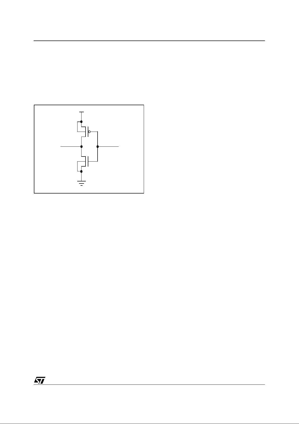
1.2.3 Termination of Unused Pins
The ST9 device is implemented using CMOS technology; therefore unused pins must be properly
terminate d in order to av oid applic ation reliability
problems. In fact, as shown in Figure 6, the standard input circuitry is based on the CMOS inverter
structure.
Figure 6. CMOS basic inverter
When an input is kept at logic zero, the N-channel
transistor is off, while the P-channel is on and can
conduct. The opposite occurs when an input is
kept at logic one. CMOS transistors are essentially
linear devices with relatively broad switching
points. During commutation, the input passes
through midsupply, and there is a region of input
voltage values where both P and N-channel transistors are on. Since normally the transitions are
fast, there is a very short time in which a current
can flow: once the s wi tchin g is co mplete d there is
no longer current. This phenomenon explains why
the overall current depends on the switching rate:
the consumption is directly proportional to the
number of transistors inside the device which are
in the linear region during transitions, charging and
discharging internal capacitances.
In order to avoid extra power supply current, it is
important to bias input pins properly when not
used. In fact, if the input impedance is very high,
pins can float, when not connected, either to a
midsupply level or can os cilla te (injecting n oise i n
the device).
Depending on the specific configuration of each
I/O pin on different ST9 devices, it can be more or
less critical to leave un used pins float ing. For this
reason, on most pins, the configuration after RESET enables an internal weak pull-up transistor in
order to avoid floating conditions. For other pins
this is intrinsically forbidden, like for the true open-
drain pins. In any case, the application software
must program the right state for unused pins to
avoid conflicts with ex ternal circuitry (whichev er it
is: pull-up, pull-down, floating, etc.).
The suggested method of termi nating unused I/O
is to connect an external individual pull-up or pulldown for each pin, e ven though initialization sof tware can force outputs to a spec ified and defined
value, during a particular phase of the RESET routine there could be an undetermined status at the
input section.
Usage of pull-ups and/or pull-downs is preferable
in place of direct connection to V
DD
or VSS. If pullup or pull-down resistors are used, inputs can be
forced for test purposes to a different value, and
outputs can be programmed to both digital levels
without generating high current drain due to the
conflict.
Anyway, during system verification flow, attention
must be paid to reviewing the connection of each
pin, in order to avoid potential problems.
1.2. 4 A voidan ce of P i n Damage
Although integrated circuit data sheets provide the
user with conservative limits and conditions in order to prevent damage, sometim es it is useful for
the hardware system designer to know the internal
failure mechanis ms: the risk of expos ure to ille gal
voltages and conditions can be reduced by smart
protection design.
It is not possible to classify and to predict all the
possible damage resulting from violating maximum ratings and conditions, due to the large
number of variables that come into play in defining
the failures: in fact, when an overvoltage condition
is applied, the effects on the device can vary s ignificantly depending on lot-to-lot process variations, operating temperature, e xternal interfacing
of the ST9 with other devices, etc.
In the following sections, background technical information is given in order to help system designers to reduce risk of damage to the ST9 device.
1.2.4.1 Electrostatic Discharge and Latchup
CMOS integrated circuits are generally sensitive
to exposure to high voltage static electricity, which
can induce permanent damage to the device: a
typical failure is the breakdown of thin oxides,
which causes high leakage current and sometimes
shorts.
Latchup is another typical phenomenon occurring
in integrated circuits: unwanted turning on of parasitic bipolar structures, or silicon-controlled rectifi-
P
N
INOUT
V
DD
V
SS
9
12/398
ST92F124/F150/F250 - GENER AL DESCRIPTION
ers (SCR), may overheat and rapi dly destroy the
device. These unintentional structures are composed of P and N regions wh ich work as em itters,
bases and collectors of parasitic bipolar transistors: the bulk resistance of the silicon in the wells
and substrate act as resistors on the SCR structure. Applying voltages below V
SS
or above VDD,
and when the level of current is able to generate a
voltage drop across the SCR parasitic resistor, the
SCR m ay be turned o n; to turn of f the SC R it is
necessary to remove the power supply from the
device.
The present ST9 design implements layout and
process solutions to decrease the effec ts of electrostatic discharges (ESD) and la tchup. Of course
it is not possible to test all devices, due to the destructive nature of the mechanism; in order to
guarantee product relia bility, destructi ve tests are
carried out on groups of devices, according to
STMicroelectronics internal Quality Assurance
standards and recommendations.
1.2.4.2 Protective Interface
Although ST9 input/output circuitry has been designed taking ESD and Latchup problems into account, for those applications an d systems where
ST9 pins are exposed to illegal voltages and h igh
current injections, the user is strongly recommended to implement ha rdware s olu tions which reduc e
the risk of damage to the microcontroller: low-pass
filters and clamp diodes are usually sufficient in
preventing stress conditions.
The risk of having out-of-range voltages an d currents is greater for those signals coming from outside the system, where noise effect or uncontrolled spikes could occur with higher probability
than for the internal signals; it must be underlined
that in some cases, adoption of filters or other dedicated interface circuitries might affect global microcontroller performance, inducing undesired timing delays, and impacting the global system
speed.
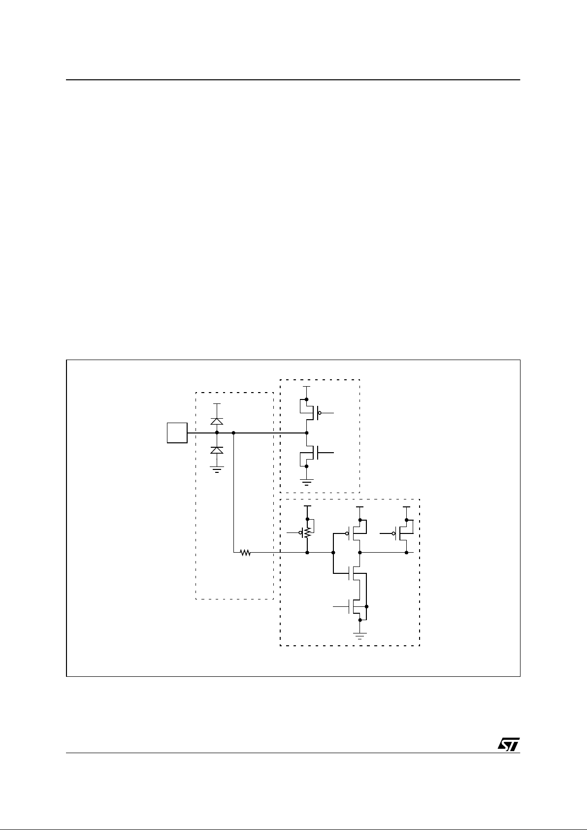
Figure 7. Digital Input/Output - Push-Pull
PIN
OUTPUT
BUFFER
P
N
P
N
N
IN PUT
BUFFER
P
ESD PROTECTION
CIRCUITRY
PORT CIRCUITRY
I/O CIRCUITRY
P
EN
EN
9
13/398
ST92F124/F150/F250 - GENER AL DESCRIPTION
1.2.4.3 Internal Circuitry: Digital I/O pin
In Figure 7 a schematic repres entation of an S T9
pin able to operate either as an input or as an output is shown. The circuitry imple men ts a stand ard
input buffer and a push-pull configuration for the
output buffer. It is evident that although it is possible to disable the output buffer when the input section is used, the MOS transistors of the buffer itself
can still affect the behaviour of the pin when exposed to illegal conditions. In f act, the P-channel
transistor of the output buffer implements a direct
diode to V
DD
(P-diffusion of the drain connected to
the pin and N-well connected to V
DD
), while the Nchannel of the output buffer implements a diode to
V
SS
(P-substrate connected to V SS and N-diffusion of the drain connected to the pin). In parallel
to these diodes, dedicated circuitry is implemented
to protect the logic from ESD events (MOS, diodes
and input series resistor).
The most important characteristic of these extra
devices is that they must not disturb normal operating modes, while acting during exposure t o over
limit conditions, avoiding permanent damage to
the logic circuitry.
All I/O pins can generally be programmed to work
also as open-drain outputs, by simply writing in the
corresponding register of the I/O Port. The gate of
the P-channel of t he o utpu t buffer i s disabl ed: it is
important to highlight that physically the P-channel
transistor is still present, so the diode to V
DD
works. In some applications it can occur that the
voltage applied to the pin is higher than the V
DD
value (supposing the external line is kept high,
while the ST9 power supply is turned off): this condition will inject current throug h the diode , risking
permanent damages to the device.
In any case, programming I/O pins as open -drain
can help when several pins in the system are tied
to the same point: of course software must pay attention to program only one of them as output at
any time, to avoid output driver contentions; it is
advisable to configure these pins a s output opendrain in order to reduce the risk of current contentions.
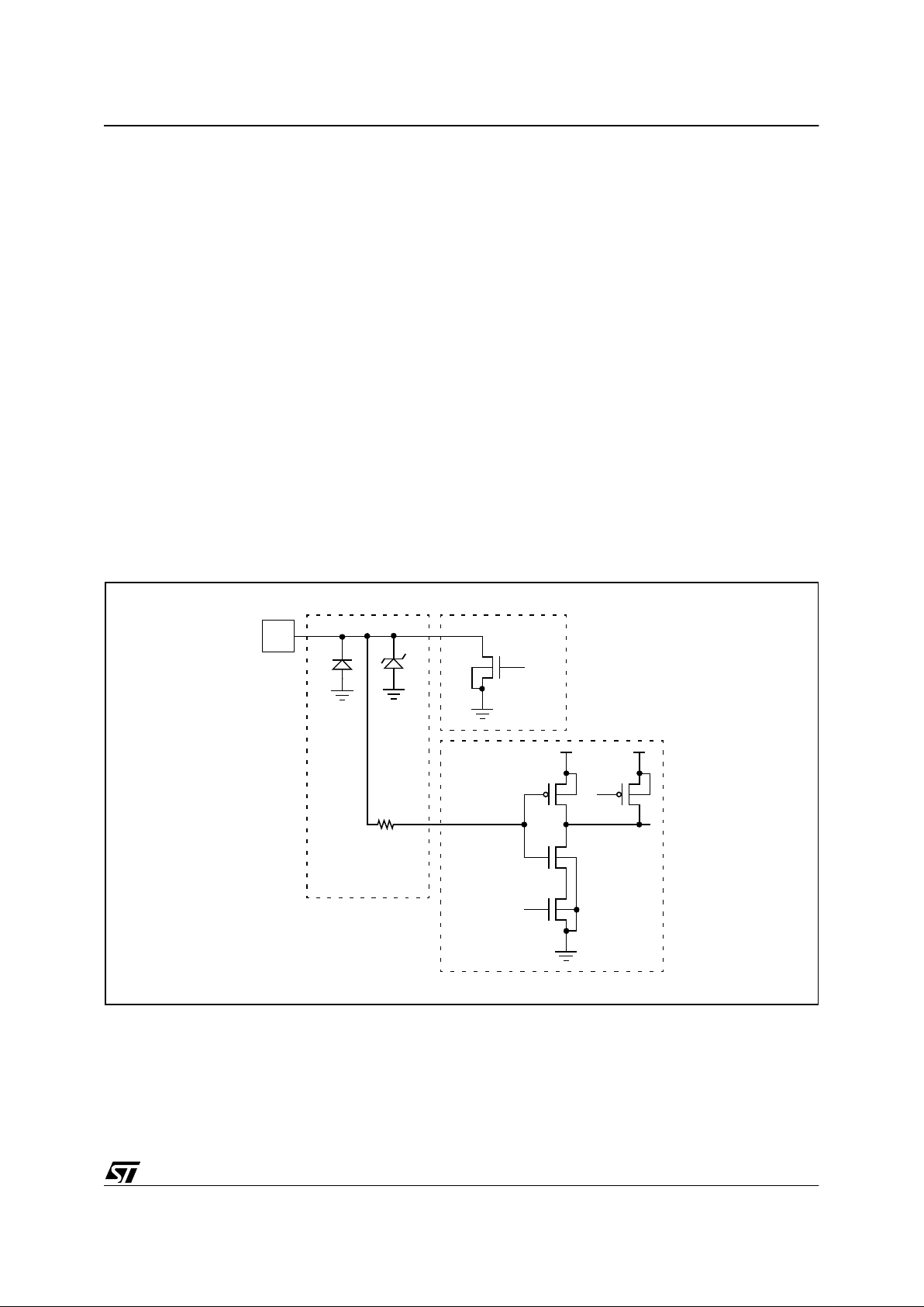
Figure 8. Digital Input/Output - True Open Drain Output
PIN
OUTPUT
BUFFER
N
P
N
N
IN P UT
BUFFER
ESD PROTECTION
CIRCUITRY
PORT CIRCUITRY
I/O CIRCUITRY
P
EN
EN
9
14/398
ST92F124/F150/F250 - GENER AL DESCRIPTION
In Figure 8 a true open-drain pin schematic is
shown. In this case all pa ths to V
DD
are removed
(P-channel driver, ESD protection diode, internal
weak pull-up) in order to allow the system to turn
off the power supply of the microcontroller and
keep the voltage level at the pin high without injecting current in the device. This is a typical condition which can occur when several devices interface a serial bus: if one device is not involved in
the communication, it can be disabled by turning
off its power supply to reduce the system current
consumption.
When an illegal negative voltage level is appl ied to
the ST9 I/O pins (both versions, push-pull and true
open-drain output) the clamp diode is always
present and active (see ESD protection circuitry
and N-channel driver).
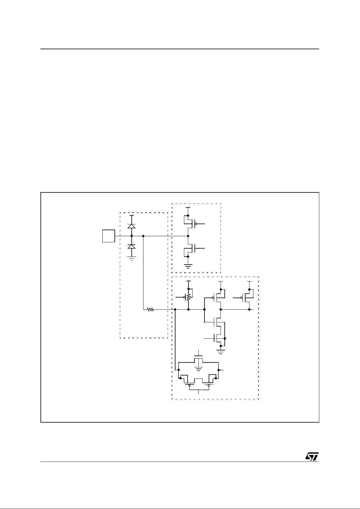
1.2.4.4 Internal Circuitry: Analog Input pin
Figure 9 shows the internal circuitry used for ana-
log input. It is substantially a digital I/O with an
added analog multipl exer for the selection of the
input channel of the Analog to Digital Converter
(ADC).
The presence of the multiplexer P-channel and Nchannel can affect the behaviour of the pin when
exposed to ille gal voltage condi tions. These transistors are controlled by a low noise logic, biased
through AV
DD
and AVSS including P-channel Nwell: it is important t o always verify the i nput vol tage value with respect to both analog power supply and digital power supply, in order to avoi d unintended current injections which (if not limited)
could destroy the device.
Figure 9. Digital Input/Output - Push-Pull Output - Analog Multiplexer Input
PIN
OUTPUT
BUFFER
P
N
P
N
N
INP UT
BUFFER
P
E
SD PROTECTION
CIRCUITRY
PORT CIRCUITRY
I/O CIRC UIT RY
P
EN
EN
N
P
P
9

15/398
ST92F124/F150/F250 - GENER AL DESCRIPTION
1.2.4.5 Power Supply and Ground
As already said for the I/O pins, in order to guarantee ST9 compliancy with respect to Quality Assu rance recommendations concerning ESD and
Latchup, dedicated circuits are added to the different power supply and ground pins (digital and analog). These structures create preferred paths for
the high current injected during discharges, avoiding damage to active logic and circuitry. It is important for the system designer to take this added circuitry into account, which is not always t ransparent with respect to the relative level of voltages applied to the different power supply and ground
pins. Figure 10 shows schematically the protection
net implemented on ST9 devices, composed of diodes and other special structures.
The clamp structure between the V
DD
and V
SS
pins is designed to be active during very fast tran-
sitions (typical of electrostat ic discharges). Other
paths are implemented throu gh diodes: they limit
the possibility of positively differentiating AV
DD
and VDD (i.e. AVDD > VDD); similar considerations
are valid for AV
SS
and VSS due to the back-toback diode structure implemented between the
two pins. Anyw ay, it mus t be highlighted t hat, because V
SS
and AVSS are connected to the substrate of the silicon die (even though in different areas of the die itself), they represent the reference
point from which all other voltages are measured,
and it is recommended to never differentiate AV
SS
from VSS.
Note: If more than one pair of pins for V
SS
and
V
DD
is available on the device, they are connected
internally and the protec tion net diagram rem ains
the same as shown in Figure 10.
Figure 10. P ower Supply an d Gro und Configurat i on
N
P
P
N
V
DD
V
SS
AV
DD
AV
SS
V
TEST
9

16/398
ST92F124/F150/F250 - GENER AL DESCRIPTION
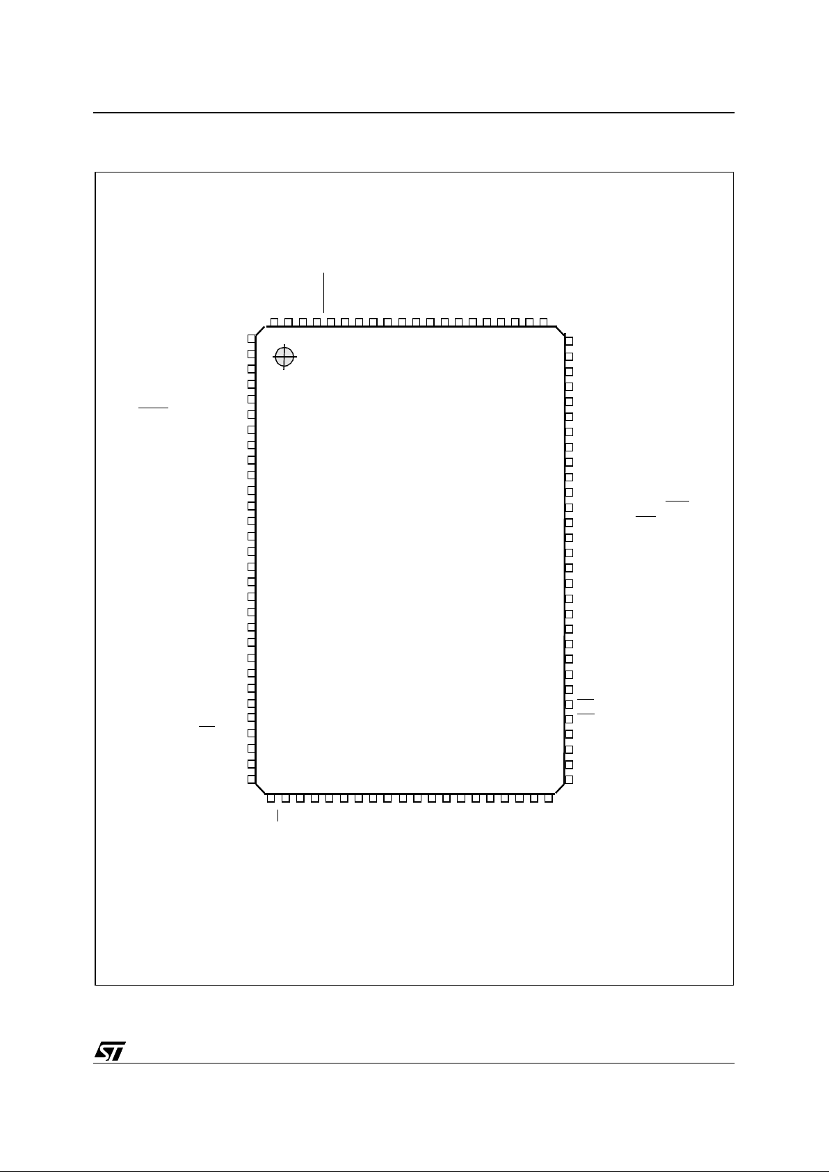
Figure 11. ST92F124/S T92 F150: Pin Configuration (Top-view TQ FP64)
TX0*/WAIT/WKUP5/P5.0
RX0*/WKU P6/WDOUT/P5.1
SIN/WKUP2 /P5.2
WDIN/SOUT /P5.3
TXCLK/CLKOUT /P5.4
RXCL0/WKUP7 /P5.5
DCD/WKUP8 /P5.6
WKUP9/RTS /P5.7
WKUP4/P4.4
EXTRG/STOUT /P4.5
SDA/P4.6
WKUP1/SCL /P4.7
S
S/P3.4
MISO/P3.5
MOSI/P3.6
SCK/WKUP0 /P3.7
HW0SW1
RESET
OSCOUT
OSCIN
VDDVSSP7.7/AIN15 /WKUP13
P7.6/AIN14 /WKUP12
P7.5/AIN13 /WKUP11
P7.4/AIN12 /WKUP3
P7.3/AIN11
P7.2/AIN10
P7.1/AIN9
P7.0/AIN8
/
CK_AF
AV
SSAVDD
N.C
P6.5/WKUP1 0/INTCLK
P6.4/NMI
P6.3/INT3/IN T5
P6.2/INT2/IN T4
P6.0/INT0/IN T1/CLOCK2/8
P0.7
P0.6
P0.5
P0.4
P0.3
P0.2
P0.1
P0.0
Reserved**
Reserved**
Reserved**
TINPA0/P2.0
TINPB0/P2.1
TOUTA0/P2.2
TOUTB0/P2.3
TINPA1/P2.4
TINPB1/P2.5
TOUTA1/P2.6
TOUTB1/P2.7
V
SS
V
DD
V
REG
V
TEST
P1.0
P1.1
P1.2
6463 62616059 58 57 56 55545352515049
48
47
46
45
44
43
42
41
40
39
38
37
36
35
34
33
1718192021222324 2930 31 3225262728
1
2
3
4
5
6
7
8
9
10
11
12
13
14
15
16
ST92F124 /
* Not available on ST92F124 version
ST92F150
1718192021222324 2930 31 3225262728
* * Reserved for ST tests, must be left unconnected
9
17/398
ST92F124/F150/F250 - GENER AL DESCRIPTION
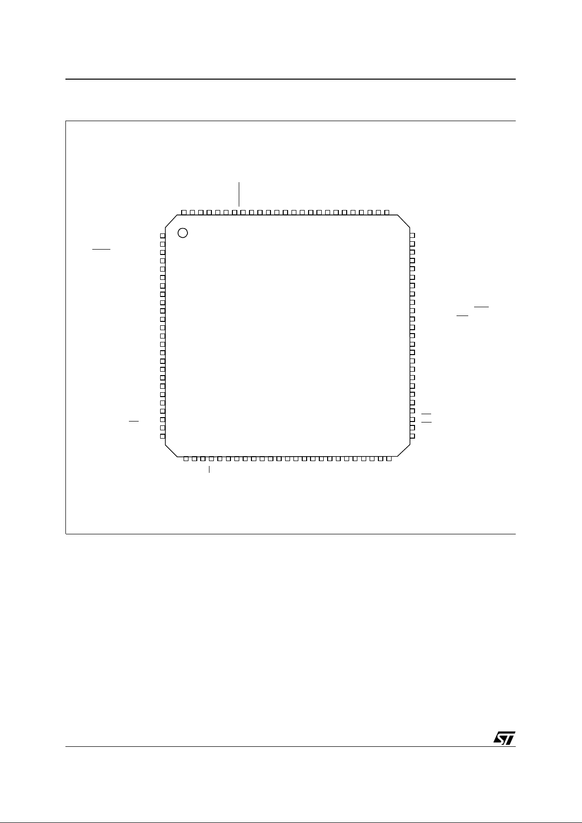
Figure 12. ST92F150: Pin Configuration (Top-view PQFP100)
A17/P9.3
A18/P9.4
A19/P9.5
A20/P9.6
A21/P9.7
TX0/WAIT
/WKUP5/P5 .0
RX0/WKUP6/ WDOUT/P5.1
SIN/WKUP2/P5 .2
WDIN/SOUT/P5 .3
TXCLK/CLKO UT/P5.4
RXCLK/WKU P7/P5.5
DCD/WKUP8/P5 .6
WKUP9/RTS/P5 .7
ICAPA1/P4.0
CLOCK2/P4 .1
OCMPA1/P4 .2
V
SS
V
DD
ICAPB1/OCMP B1/P4.3
EXTCLK1/WKU P4/P4.4
EXTRG/STO UT/P4.5
SDA/P4.6
WKUP1/SCL/P4 .7
ICAPB0/P3.1
ICAPA0/OCMP A0/P3.2
OCMPB0/P3 .3
EXTCLK0/S S
/P3.4
MISO/P3.5
MOSI/P3.6
SCK/WKUP0/P3 .7
P9.2/A16
P9.1/TDO
P9.0/RDI
HW0SW1
RESET
OSCOUT
OSCIN
VDDVSSP7.7/AIN15/7/W KUP13
P7.6/AIN14/WK UP12
P7.5/AIN13/WK UP11
P7.4/AIN12/WK UP3
P7.3/AIN11
P7.2/AIN10
P7.1/AIN9
P7.0/AIN8
/
CK_AF
AV
SSAVDD
P8.7/AIN7
P8.6/AIN6
P8.5/AIN5
P8.4/AIN4
P8.3/AIN3
P8.2/AIN2
P8.1/AIN1/WKU P15
P8.0/AIN0/WKU P14
VPWO*
P6.5/WKUP10/I NTCLK/VPW
P6.4/NMI
P6.3/INT3/INT5
P6.2/INT2/INT4 /DS2
P6.1/INT6/RW
P6.0/INT0/INT1 /CLOCK2/8
P0.7/A7/D7
V
DD
V
SS
P0.6/A6/D6
P0.5/A5/D5
P0.4/A4/D4
P0.3/A3/D3
P0.2/A2/D2
P0.1/A1/D1
P0.0/A0/D0
AS
DS
P1.7/A15
P1.6/A14
P1.5/A13
P1.4/A12
V
REG
RW
TINPA0/P2.0
TINPB0/P2.1
TOUTA0/P2.2
TOUTB0/P2.3
TINPA1/P2.4
TINPB1/P2.5
TOUTA1/P2.6
TOUTB1/P2.7
V
SS
V
DD
V
REG
V
TEST
A8/P1.0
A9/P1.1
A10/P1.2
A11/P1.3
**RX1/WKUP6
**TX1
1
50
30
ST92F150
2
3
4
5
6
7
8
9
10
11
12
13
14
15
16
17
18
19
20
21
22
23
24
25
26
27
28
29
80
51
79
78
77
76
75
74
73
72
71
70
69
68
67
66
65
64
63
62
61
60
59
58
57
56
55
54
53
52
49484746454443424140393837363534333231
81
828384858687888990919293
94
9596979899100
*On devices without JPBLD peripheral, this pin must not be connected.
**On devices without CAN1 peripheral, these pins must not be connected.
9
18/398
ST92F124/F150/F250 - GENER AL DESCRIPTION
Figure 13. ST92F150: Pin Configuration (Top-view TQ FP100)
* V
TEST
must be kept low in standard operating mode.
**On devices without CAN1 peripheral, these pins must not be connected.
1
2
3
4
5
6
7
8
9
10
11
12
13
14
15
16
17
18
19
20
21
22
23
24
25
26
2728 29 3031 3233 343536 3738 39 4041 4243 4445 46 4748 4950
75
74
73
72
71
70
69
68
67
66
65
64
63
62
61
60
59
58
57
56
55
54
53
52
51
10099 98 9796 9594 9392 91 9089 8887 868584 8382 81 8079 7877 76
ST92F150
P8.4/AIN4
P8.3/AIN3
P8.2/AIN2
P8.1/AIN1/WKUP15
P8.0/AIN0/WKUP14
VPWO
P6.5/WKUP10/INTCLK/VPW
P6.4/NMI
P6.3/INT3/INT5
P6.2/INT2/INT4/DS2
P6.1/INT6/RW
P6.0/INT0/INT1/CLOCK2/8
P0.7/A7/D7
V
DD
V
SS
P0.6/A6/D6
P0.5/A5/D5
P0.3/A3/D3
P0.2/A2/D2
P0.1/A1/D1
P0.0/A0/D0
AS
DS
P0.4/A4/D4
P1.7/A15
A20/P9.6
TX0/WAIT
/WKUP5/P5.0
RX0/WKUP6/WDOUT/P5.1
TXCLK/CLKOUT/P5.4
OCMPA1/P4.2
V
DD
A21/P9.7
WDIN/SOUT/P5.3
DCD/WKUP8/P5.6
V
SS
ICAPB1/OCMPB1/P4.3
SDA/P4.6
SIN/WKUP2/P5.2
RXCLK/WKUP7/P5.5
CLOCK2/P4.1
EXTCLK1/WKUP4/P4.4
ICAPB0/P3.1
ICAPA0/OCMPA0/P3.2
WKUP9/RTS/P5.7
ICAPA1/P4.0
EXTRG/STOUT/P4.5
WKUP1/SCL/P4.7
OCMPB0/P3.3
EXTCLK0/SS
/P3.4
MISO/P3.5
P9.5/A19
P9.4/A18
P9.2/A16
HW0SW1
P7.7/AIN15/7/WKUP13
P7.4/AIN12/WKUP3
P9.3/A17
P9.0/RDI
RESET
P7.6/AIN14/WKUP12
P7.5/AIN13/WKUP11
P7.1/AIN9
P9.1/TDO
OSCIN
V
SS
P7.3/AIN11
P7.0/AIN8/CK_AF
P8.7/AIN7
OSCOUT
V
DD
P7.2/AIN10
AVSSAVDDP8.6/AIN6
P8.5/AIN5
MOSI/P3.6
SCK/WKUP0/P3.7
RW
TOUTA0/P2.2
V
SS
*V
TEST
V
REG
TINPB0/P2.1
TOUTB0/P2.3
V
DD
V
REG
A10/P1.2
TINPA0/P2.0
TINPB1/P2.5
TOUTB1/P2.7
A8/P1.0
A11/P1.3
A12/P1.4
TINPA1/P2.4
TOUTA1/P2.6
A9/P1.1
**RX1/WKUP6
**TX1
A13/P1.5
A14/P1.6
9

19/398
ST92F124/F150/F250 - GENER AL DESCRIPTION
Figure 14. ST92F250: Pin Configuration (Top-view PQFP100)
* V
TEST
must be kept low in standard operating mode.
SDA1/A17/P9.3
SCL1/A18/P9.4
A19/P9.5
A20/P9.6
A21/P9.7
TX0/WAIT
/WKUP5/P5.0
RX0/WKUP6/WDOUT/P5.1
SIN/WKUP2/P5.2
WDIN/SOUT/P5.3
TXCLK/CLKOUT/P5.4
RXCLK/WKUP7/P5.5
DCD/WKUP8/P5.6
WKUP9/RTS/P5.7
ICAPA1/P4.0
CLOCK2/P4.1
OCMPA1/P4.2
V
SS
V
DD
ICAPB1/OCMPB1/P4.3
EXTCLK1/WKUP4/P4.4
EXTRG/STOUT/P4.5
SDA0/P4.6
WKUP1/SCL0/P4.7
ICAPB0/P3.1
ICAPA0/OCMPA0/P3.2
OCMPB0/P3.3
EXTCLK0/SS
/P3.4
MISO/P3.5
MOSI/P3.6
SCK/WKUP0/P3.7
P9.2/A16
P9.1/TDO
P9.0/RDI
HW0SW1
RESET
OSCOUT
OSCIN
VDDVSSP7.7/AIN15/7/WKUP13
P7.6/AIN14/WKUP12
P7.5/AIN13/WKUP11
P7.4/AIN12/WKUP3
P7.3/AIN11
P7.2/AIN10
P7.1/AIN9
P7.0/AIN8/CK_AF
AVSSAVDDP8.7/AIN7
P8.6/AIN6
P8.5/AIN5
P8.4/AIN4
P8.3/AIN3
P8.2/AIN2
P8.1/AIN1/WKUP15
P8.0/AIN0/WKUP14
P3.0
P6.5/WKUP10/INTCLK
P6.4/NMI
P6.3/INT3/INT5
P6.2/INT2/INT4/DS2
P6.1/INT6/RW
P6.0/INT0/INT1/CLOCK2/8
P0.7/A7/D7
V
DD
V
SS
P0.6/A6/D6
P0.5/A5/D5
P0.4/A4/D4
P0.3/A3/D3
P0.2/A2/D2
P0.1/A1/D1
P0.0/A0/D0
AS
DS
P1.7/A15
P1.6/A14
P1.5/A13
P1.4/A12
V
REG
RW
TINPA0/P2.0
TINPB0/P2.1
TOUTA0/P2.2
TOUTB0/P2.3
TINPA1/P2.4
TINPB1/P2.5
TOUTA1/P2.6
TOUTB1/P2.7
V
SS
V
DD
V
REG
*V
TEST
A8/P1.0
A9/P1.1
A10/P1.2
A11/P1.3
P6.6
P6.7
1
50
30
ST92F250
2
3
4
5
6
7
8
9
10
11
12
13
14
15
16
17
18
19
20
21
22
23
24
25
26
27
28
29
80
51
79
78
77
76
75
74
73
72
71
70
69
68
67
66
65
64
63
62
61
60
59
58
57
56
55
54
53
52
49484746454443424140393837363534333231
81
828384858687888990919293949596979899100
9

20/398
ST92F124/F150/F250 - GENER AL DESCRIPTION
Figure 15. ST92F250: Pin Configuration (Top-view TQ FP100)
* V
TEST
must be kept low in standard operating mode.
1
2
3
4
5
6
7
8
9
10
11
12
13
14
15
16
17
18
19
20
21
22
23
24
25
26
2728 29 3031 3233 3435 36 3738 3940 4142 43 4445 4647 48 49 50
75
74
73
72
71
70
69
68
67
66
65
64
63
62
61
60
59
58
57
56
55
54
53
52
51
10099 98 97 96 9594 9392 91 9089 8887 8685 84 8382 8180 7978 7776
ST92F250
P8.4/AIN4
P8.3/AIN3
P8.2/AIN2
P8.1/AIN1/WKUP15
P8.0/AIN0/WKUP14
P3.0
P6.5/WKUP10/INTCLK
P6.4/NMI
P6.3/INT3/INT5
P6.2/INT2/INT4/DS2
P6.1/INT6/RW
P6.0/INT0/INT1/CLOCK2/8
P0.7/A7/D7
V
DD
V
SS
P0.6/A6/D6
P0.5/A5/D5
P0.3/A3/D3
P0.2/A2/D2
P0.1/A1/D1
P0.0/A0/D0
AS
DS
P0.4/A4/D4
P1.7/A15
A20/P9.6
TX/WAIT
/WKUP5/P5.0
RX/WKUP6/WDOUT/P5.1
TXCLK/CLKOUT/P5.4
OCMPA1/P4.2
V
DD
A21/P9.7
WDIN/SOUT/P5.3
DCD/WKUP8/P5.6
V
SS
ICAPB1/OCMPB1/P4.3
SDA0/P4.6
SIN/WKUP2/P5.2
RXCLK/WKUP7/P5.5
CLOCK2/P4.1
EXTCLK1/WKUP4/P4.4
ICAPB0/P3.1
ICAPA0/OCMPA0/P3.2
WKUP9/RTS/P5.7
ICAPA1/P4.0
EXTRG/STOUT/P4.5
WKUP1/SCL0/P4.7
OCMPB0/P3.3
EXTCLK0/SS
/P3.4
MISO/P3.5
P9.5/A19
P9.4/A18/SCL1
P9.2/A16
HW0SW1
P7.7/AIN15/7/WKUP13
P7.4/AIN12/WKUP3
P9.3/A17/SDA1
P9.0/RDI
RESET
P7.6/AIN14/WKUP12
P7.5/AIN13/WKUP11
P7.1/AIN9
P9.1/TDO
OSCIN
V
SS
P7.3/AIN11
P7.0/AIN8/CK_AF
P8.7/AIN7
OSCOUT
V
DD
P7.2/AIN10
AVSSAVDDP8.6/AIN6
P8.5/AIN5
MOSI/P3.6
SCK/WKUP0/P3.7
RW
TOUTA0/P2.2
V
SS
*V
TEST
V
REG
TINPB0/P2.1
TOUTB0/P2.3
V
DD
V
REG
A10/P1.2
TINPA0/P2.0
TINPB1/P2.5
TOUTB1/P2.7
A8/P1.0
A11/P1.3
A12/P1.4
TINPA1/P2.4
TOUTA1/P2.6
A9/P1.1
P6.6
P6.7
A13/P1.5
A14/P1.6
9
21/398
ST92F124/F150/F250 - GENER AL DESCRIPTION
Table 1. ST92F124/F 150/F250 Power Supply Pins
Table 2. ST92F124/F150/F250 Primary Function Pins
Note 1: ST92F150JDV1 only.
Name Function TQFP64 P QFP100 TQFP100
V
DD
Main Power Supply Voltage
(Pins internally connected)
-1815
27 42 39
-6562
60 93 90
V
SS
Digital Circuit Ground
(Pins internally connected)
-1714
26 41 38
-6461
59 92 89
AV
DD
Analog Circuit Supply Voltage 49 82 79
AV
SS
Analog Circuit Ground 50 83 80
V
TEST
Must be kept low in standard operating mode 29 44 41
V
REG
Stabilization capacitor(s) for internal voltage regulator 28
31
43
28
40
Name Function TQFP64 PQFP100 TQFP100
AS
Address Strobe - 56 53
DS
Data Strobe - 55 52
RW
Read/Write - 32 29
OSCIN Crystal Oscillator Input 61 94 91
OSCOUT Crystal Oscillator Output 62 95 92
RESET
Reset to initialize the Microcontroller 63 96 93
HW0SW1 Watchdog HW/SW enabling selection 64 97 94
VPWO
1)
J1850 JBLPD Output - 73 70
RX1/WKUP6
1)
CAN1 Receive Data / Wake-up Line 6 - 49 46
TX1
1)
CAN1 Transmit Data. - 50 47
9
22/398
ST92F124/F150/F250 - GENER AL DESCRIPTION
1.3 VOLTAGE REGULATOR
The internal Voltage Regulator (VR) is used to
power the microcontroller starting from the external power supply. The VR comprises a M ain voltage regulator and a Low-power regulator.
– The Mai n voltage regulator generates sufficient
current for the microcontroller to operate in any
mode. It has a static power consum ption (300
µA typ.).
– The separate Low-Power regulator consumes
less power is used only wh en t he m icrocont roller is in Low Power mode. It has a different design from the main VR a nd generates a lower,
non-stabilized and non- ther m ally- com pens at ed
voltage sufficient for maintaining the data in
RAM and the Register File.
For both the Main VR and the Low-Power VR, stabilization is achieved by an external capacitor,
connected to on e of the V
REG
pins. The minimum
recommended value is 300 nF, and care must be
taken to minimize distance between the chip and
the capacitor. Care should also be taken to limit
the serial inductance to less than 60nH.
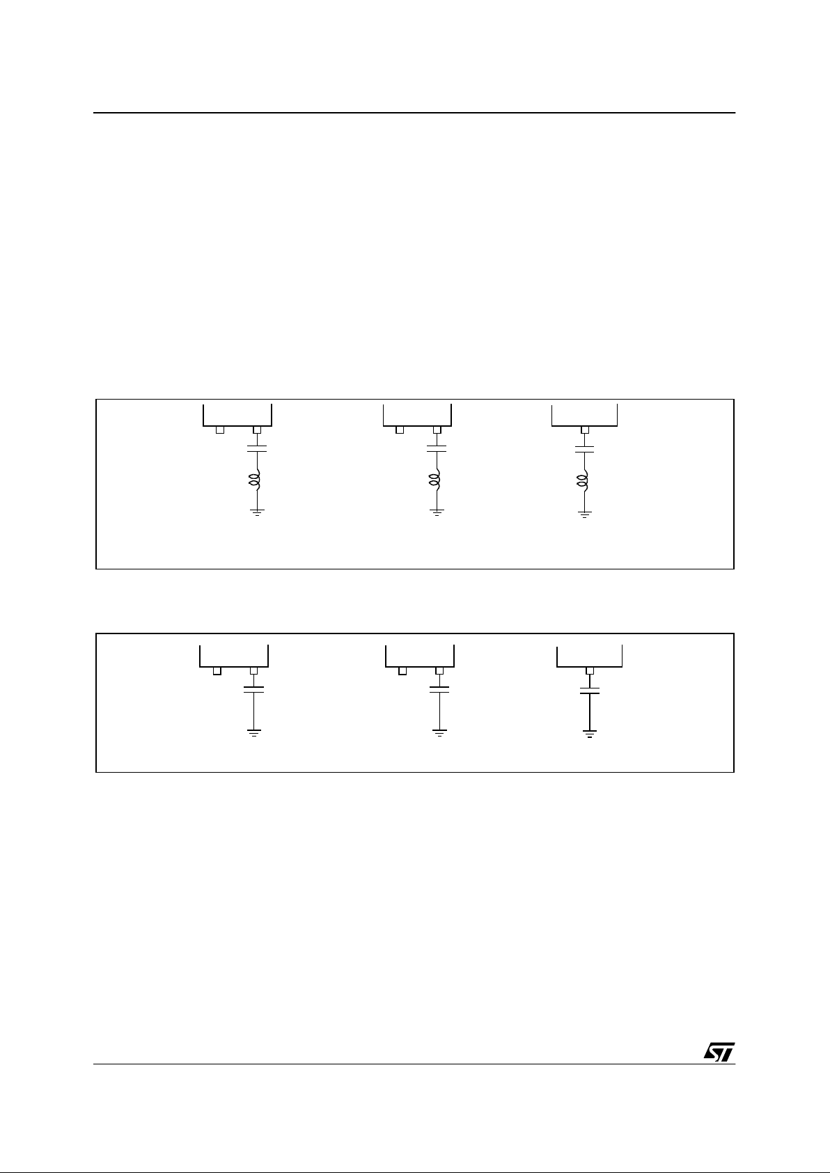
Figure 16. Recommended Connections for V
REG
IMPORTANT: The V
REG
pin cannot be used to drive external devices.
Figure 17. Minimum Required Connections for V
REG
Note: Pin 31 of PQFP100 or pin 28 of TQFP100 can be left unconnnected. A secondary stabilization net-
work can also be connected to these pins.
PQFP100
QFP64
C
L
L = Ferrite bead for EMI protection.
Pin 28
C
L
Pin 43
Pin 31
TQFP100
C
L
Pin 40
Pin 28
Suggested type: Murata BLM18BE601FH1: (Imp. 600 Ω at 100 M Hz).
C = 300 to 600nF
C
PQFP100 QFP64
C
Pin 43Pin 31 Pin 28
C
TQFP100
Pin 40Pin 28
C = 300 to 600nF
9
23/398
ST92F124/F150/F250 - GENER AL DESCRIPTION
1.4 I/O PORTS
Port 0, Port 1 and Port 9[7:2] provide the external
memory interface. All the ports of the device ca n
be programmed as Inp ut/Output or i n I nput m ode,
compatible with TTL or CMOS levels (except
where Schmitt Trigger is present). Each bit can be
programmed individually (Refer to the I/O ports
chapter).
Internal Weak Pull-up
As shown in Table 3, not all input sections imple-
ment a Weak P ull-up. Thi s m eans that t he pull -up
must be connected externally when the p in is not
used or programmed as bidirectional.
TTL/CMO S I np ut
For all those port bits where no input schmitt trigger is implemented, it is always possible to program the input level as TTL or CMOS compatible
by programming the relevant PxC2.n control bit.
Refer I/O Ports Chapter to the section titled “Input/
Output Bit Configuration”.
Schmitt Tr ig ger I nput
Two different kinds of Schmitt Trigger circuitries
are implemented: Standard and High Hysteresis.
Standard Schmitt Trigger is w idely used (see Ta-
ble 3), while the High Hysteresis Schmitt Trigger is
present on ports P4[7:6] and P6[5:4].
All inputs which can be used for detecting interrupt
events have been configured with a “Standard”
Schmitt Trigger, apart from the NMI pin which i mplements the “High Hysteresis” version. In this
way, all interrupt lines are guaranteed as “level
sensitive”.
Push-Pull/OD Output
The output buffer can be programmed as pushpull or open-drain: attention must be paid to the
fact that the open-drain option corresponds only to
a disabling of P-channel MOS transistor of the
buffer itself: it is still present and physically connected to the pin. Consequently it is not possible to
increase the output voltage on the pin over
V
DD
+0.3 Volt, to avoid direct junction biasing.
Pure Open-Drain Output
The user can increase t he voltage on an I/O pin
over V
DD
+0.3 Volt where the P-channel MOS transistor is physically absent: this is allowed on all
“Pure Open Drain” pins. In this case, the push-pull
option is not available and a ny weak pull-up m ust
be implemented externally.
Table 3. I/O Port Characteristics
Legend: WPU = Weak Pull-Up, OD = Open Drain.
Note 1: Port 3.0 and Port6 [7:6] present on ST92F250 version only.
Input Output Weak Pull-Up Reset State
Port 0[7:0] TTL/CMOS Push-Pull/OD No Bidirectional
Port 1[7:0] TTL/CMOS Push-Pull/OD No Bidirectional
Port 2[1:0]
Port 2[3:2]
Port 2[5:4]
Port 2[7:6]
Schmitt trigger
TTL/CMOS
Schmitt trigger
TTL/CMOS
Push-Pull/OD
Pure OD
Push-Pull/OD
Push-Pull/OD
Yes
No
Yes
Yes
Input
Input CMOS
Input
Input CMOS
Port 3[2:0]
1)
Port 3.3
Port 3[7:4]
Schmitt trigger
TTL/CMOS
Schmitt trigger
Push-Pull/OD
Push-Pull/OD
Push-Pull/OD
Yes
Yes
Yes
Input
Input CMOS
Input
Port 4.0, Port 4.4
Port 4.1
Port 4.2, Port 4.5
Port 4.3
Port 4[7:6]
Schmitt trigger
Schmitt trigger
TTL/CMOS
Schmitt trigger
High hysteresis Schmitt trigger
Push-Pull/OD
Push-Pull/OD
Push-Pull/OD
Push-Pull/OD
Pure OD
No
Yes
Yes
Yes
No
Input
Bidirectional WPU
Input CMOS
Input
Input
Port 5[2:0], Port 5[7:4]
Port 5.3
Schmitt trigger
TTL/CMOS
Push-Pull/OD
Push-Pull/OD
No
Yes
Input
Input CMOS
Port 6[3:0]
Port 6[5:4]
Port 6[7:6]
1)
Schmitt trigger
High hysteresis Schmitt trigger
Schmitt trigger
Push-Pull/OD
Push-Pull/OD
Push-Pull/OD
Yes
Yes
Yes
Input
Input
Input
Port 7[7:0] Schmitt trigger Push-Pull/OD Yes Input
Port 8[1:0]
Port 8[7:2]
Schmitt trigger
Schmitt trigger
Push-Pull/OD
Push-Pull/OD
Yes
Yes
Input
Bidirectional WPU
Port 9[7:0] Schmitt trigger Push-Pull/OD Yes Bidirectional WPU
9

24/398
ST92F124/F150/F250 - GENER AL DESCRIPTION
How to Configure the I/O Ports
To configure the I/O ports, use the information in
Table 3, Table 4 and the Port Bit Configuration Ta-
ble in the I/O Ports Chapter (See page 149).
Input Note = the hardware characteristics fixed for
each port line in Table 3.
– If Input note = TTL/CMOS, either TTL or CMOS
input level can be selected by software.
– If Input note = Schmitt trigger, selecting CMOS
or TTL input by software has no effect, the input
will always be Schmit t Trigger.
Alternate Functions (AF) = More than one AF
cannot be assigned to an I/O pin at the same time:
An alternate function can be selected as follows.
AF Inputs:
– AF is selected implicitly by enabling the corre-
sponding peripheral. Exception to this are ADC
inputs which must be explicitly selected as AF in-
put by software.
AF Outputs or Bidirectional Lines:
– In the case of Outputs or I/Os, AF is selected ex-
plicitly by sof twar e.
Example 1: SCI-M input
AF: SIN, Port: P5.2. Schmitt Trigger input.
Write the port configuration bits:
P5C2.2=1
P5C1.2=0
P5C0.2 =1
Enable the SCI peripheral by software as described in the SCI chapter.
Example 2: SCI-M output
AF: SOUT, Port: P5.3, Push-Pull/OD output.
Write the port configuration bits (for AF OUT PP):
P5C2.3=0
P5C1.3=1
P5C0.3 =1
Example 3: External Memory I/O
AF: A0/D0, Port : P0.0, Input Note: TTL/CMOS in-
put.
Write the port configuration bits:
P0C2.0=1
P0C1.0=1
P0C0.0 =1
Example 4: Analog input
AF: AIN8, Port : 7.0, Analog input.
Write the port configuration bits:
P7C2.0=1
P7C1.0=1
P7C0.0 =1
9

25/398
ST92F124/F150/F250 - GENER AL DESCRIPTION
1.5 Alternat e Functions for I/O Ports
All the ports in the following table are useable for general purpose I/O (input, output or bidirectional).
Table 4. I/O Port Alternate Functions
Port
Name
Pin No.
Alternate Functions
TQFP64 PQFP100 TQFP100
P0.0 - 57 54 A0/D0 I/O Address/Data bit 0
P0.1 - 58 55 A1/D1 I/O Address/Data bit 1
P0.2 - 59 56 A2/D2 I/O Address/Data bit 2
P0.3 - 60 57 A3/D3 I/O Address/Data bit 3
P0.4 - 61 58 A4/D4 I/O Address/Data bit 4
P0.5 - 62 59 A5/D5 I/O Address/Data bit 5
P0.6 - 63 60 A6/D6 I/O Address/Data bit 6
P0.7 - 66 63 A7/D7 I/O Address/Data bit 7
P1.0 - 45 42 A8 I/O Address bit 8
P1.1 - 46 43 A9 I/O Address bit 9
P1.2 - 47 44 A10 I/O Address bit 10
P1.3 - 48 45 A11 I/O Address bit 11
P1.4 - 51 48 A12 I/O Address bit 12
P1.5 - 52 49 A13 I/O Address bit 13
P1.6 - 53 50 A14 I/O Address bit 14
P1.7 - 54 51 A15 I/O Address bit 15
P2.0 18 33 30 TINPA0 I Multifunction Timer 0 - Input A
P2.1 19 34 31 TINPB0 I Multifunction Timer 0 - Input B
P2.2 20 35 32 TOUTA0 O Multifunction Timer 0 - Output A
P2.3 21 36 33 TOUTB0 O Multifunction Timer 0 - Output B
P2.4 22 37 34 TINPA1 I Multifunction Timer 1 - Input A
P2.5 23 38 35 TINPB1 I Multifunction Timer 1 - Input B
P2.6 24 39 36 TOUTA1 O Multifunction Timer 1 - Output A
P2.7 25 40 37 TOUTB1 O Multifunction Timer 1 - Output B
P3.0
1)
-7370
P3.1 - 24 21 ICAPB0 I Ext. Timer 0 - Input Capture B
P3.2 - 25 22
ICAPA0 I Ext. Timer 0 - Input Capture A
OCMPA0 O Ext. Timer 0 - Output Compare A
P3.3 - 26 23 OCMPB0 O Ext. Timer 0 - Output Compare B
P3.4 - 27 24
EXTCLK0 I Ext. Timer 0 - Input Clock
SS I SPI - Slave Select
P3.5 14 28 25 MISO I/O SPI - Master Input/Slave Output Data
P3.6 15 29 26 MOSI I/O SPI - Master Output/Slave Input Data
9

26/398
ST92F124/F150/F250 - GENER AL DESCRIPTION
P3.7 16 30 27
SCK I SPI - Serial Input Clock
WKUP0 I Wake-up Line 0
SCK O SPI - Serial Output Clock
P4.0 - 14 11 ICAPA1 I Ext. Timer 1 - Input Capture A
P4.1 - 15 12 CLOCK2 O CLOCK2 internal signal
P4.2 - 16 13 OCMPA1 O Ext. Timer 1 - Output Compare A
P4.3 - 19 16
ICAPB1 I Ext. Timer 1 - Input Capture B
OCMPB1 O Ext. Timer 1 - Output Compare B
P4.4 - 20 17
EXTCLK1 I Ext. Timer 1 - Input Clock
WKUP4 I Wake-up Line 4
P4.5 10 21 18
EXTRG I ADC Ext. Trigger
STOUT O Standard Timer Output
P4.6 11 22 19 SDA0 I/O I
2
C 0 Data
P4.7 12 23 2 0
WKUP1 I Wake-up Line 1
SCL0 I/O I
2
C 0 Clock
P5.0 1 6 3
WAIT
I External Wait Request
WKUP5 I Wake-up Line 5
TX0
1)
O CAN 0 output
P5.1 2 7 4
WKUP6 I Wake-up Line 6
RX0
1)
I CAN 0 input
WDOUT O Watchdog Timer Output
P5.2 3 8 5
SIN0 I SCI-M - Serial Data Input
WKUP2 I Wake-up Line 2
P5.3 4 9 6
WDIN I Watchdog Timer Input
SOUT O SCI-M - Serial Data Output
P5.4 5 10 7
TXCLK I SCI-M - Transmit Clock Input
CLKOUT O SCI-M - Clock Output
P5.5 6 11 8
RXCLK I SCI-M - Receive Clock Input
WKUP7 I Wake-up Line 7
P5.6 7 12 9
DCD I SCI-M - Data Carrier Detect
WKUP8 I Wake-up Line 8
P5.7 8 13 10
WKUP9 I Wake-up Line 9
RTS O SCI-M - Request To Send
P6.0 43 67 64
INT0 I Ext ernal Interr upt 0
INT1 I Ext ernal Interr upt 1
CLOCK2/8 O CLOCK2 divided by 8
P6.1 - 68 65
INT6 I Ext ernal Interr upt 6
RW
O Read/Wr ite
Port
Name
Pin No.
Alternate Functions
TQFP64 PQFP100 TQFP100
9

27/398
ST92F124/F150/F250 - GENER AL DESCRIPTION
P6.2 44 69 66
INT2 I Ext ernal Interr upt 2
INT4 I Ext ernal Interr upt 4
DS2 O Data Strobe 2
P6.3 45 70 67
INT3 I Ext ernal Interr upt 3
INT5 I Ext ernal Interr upt 5
P6.4 46 71 68 NMI I Non Maskable Interrupt
P6.5 47 72 69
WKUP10 I Wake-up Line 10
VPWI
1)
I JBLPD input
INTCLK O Internal Main Clock
P6.6
1)
-4946
P6.7
1)
-5047
P7.0 51 84 81
AIN8 I Analog Data Input 8
CK_AF I Clock Alternative Source
P7.1 52 85 82 AIN9 I Analog Data Input 9
P7.2 53 86 83 AIN10 I Analog Data Input 10
P7.3 54 87 84 AIN11 I Analog Data Input 11
P7.4 55 88 85
WKUP3 I Wake-up Line 3
AIN12 I Analog Data Input 12
P7.5 56 89 86
AIN13 I Analog Data Input 13
WKUP11 I Wake-up Line 11
P7.6 57 90 87
AIN14 I Analog Data Input14
WKUP12 I Wake-up Line 12
P7.7 58 91 88
AIN15 I Analog Data Input 15
WKUP13 I Wake-up Line 13
P8.0 - 74 71
AIN0 I Analog Data Input 0
WKUP14 I Wake-up Line 14
P8.1 - 75 72
AIN1 I Analog Data Input 1
WKUP15 I Wake-up Line 15
P8.2 - 76 73 AIN2 I Analog Data Input 2
P8.3 - 77 74 AIN3 I Analog Data Input 3
P8.4 - 78 75 AIN4 I Analog Data Input 4
P8.5 - 79 76 AIN5 I Analog Data Input 5
P8.6 - 80 77 AIN6 I Analog Data Input 6
P8.7 - 81 78 AIN7 I Analog Data Input 7
P9.0 - 98 95 RDI
1)
I SCI-A Receive Data Input
P9.1 - 99 96 TDO
1)
O SCI-A Transmit Data Output
P9.2 - 100 97 A16 O Address bit 16
Port
Name
Pin No.
Alternate Functions
TQFP64 PQFP100 TQFP100
9

28/398
ST92F124/F150/F250 - GENER AL DESCRIPTION
Note 1: Available on some devices only. Note 2: For the ST92F250 device, since A [18:17]
share the same pins as SDA1 and SCL1 of I²C_1,
these address bits are not available when the
I²C_1 is in use (when I2CCR.PE bit is set).
P9.3 - 1 9 8
A17
2)
O Address bit 17
SDA1
1)
I/O I²C 1 Data
P9.4 - 2 9 9
A18
2)
O Address bit 18
SCL1
1)
I/O I²C 1 Clock
P9.5 - 3 100 A19 O Address bit 19
P9.6 - 4 1 A20 O Address bit 20
P9.7 - 5 2 A21 O Address bit 21
Port
Name
Pin No.
Alternate Functions
TQFP64 PQFP100 TQFP100
9

29/398
ST92F124/F150/F250 - GENER AL DESCRIPTION
1.6 OPERATING MODES
To optimize the performance versus the power
consumption of the device, the ST92F124/F150/
F250 supports different ope rating m odes that can
be dynamically selected depending on the performance and functionality requirements of the application at a given moment.
RUN MODE: This is the full speed execution mode
with CPU and peripherals running at the maximum
clock speed delivered by the Phase Lo cked Loo p
(PLL) of the Clock Control Unit (CCU).
SLOW MODE: Power consumption can be significantly reduced by running the CPU and the peripherals at reduced clock speed us ing the CPU
Prescaler and CCU Clock Divider.
WAIT FOR INTERRUPT MODE: The Wait For Interrupt (WFI) instruction suspends program execution until an interrupt request is ac knowledged.
During WFI, the CPU clock is halted while the peripheral and interrupt controller keep running at a
frequency depending on the CCU programming.
LOW POWER WAIT FOR INTERRUPT MODE:
Combining SLOW mode and Wait For Interrupt
mode it is possible to reduce the power consum ption by more than 80%.
STOP MODE: When the STOP is requested by
executing the STOP bit writing sequence (see
dedicated section on Wake-up Management Unit
paragraph), and if NMI is kept low, the CPU and
the peripherals stop operating. Operations resume
after a wake-up line is activated (16 wake-up lines
plus NMI pin). See the RCCU and Wake-up Management Unit paragraphs i n the following for the
details. The difference with the HALT mode consists in the way the CPU exits this state: when the
STOP is executed, the status of the registers is recorded, and when the system exits from the STOP
mode the CPU continues the execution with the
same status, without a system reset.
When the MCU enters STOP mode the Watchdog
stops counting. After the MCU exits from STOP
mode, the Watchdog resumes counting from
where it left off.
When the MCU exits from STOP mode, the oscillator, which was sleeping too, requires about 5 ms
to restart working prope rly (at a 4 MHz oscillator
frequency). An internal counter is pre sent to guarantee that all operations after exiting STOP Mode,
take place with the clock stabilised.
The counter is active only when the oscillation has
already taken place. This means that 1-2 ms must
be added to take into account the first phase of the
oscillator restart.
HALT MODE: When executing the HALT instruction, and if the W atchdo g is not enabled, the CPU
and its peripherals stop operating and the status of
the machine remains frozen (the clock is also
stopped). A reset is necessary to exit from Halt
mode.
9
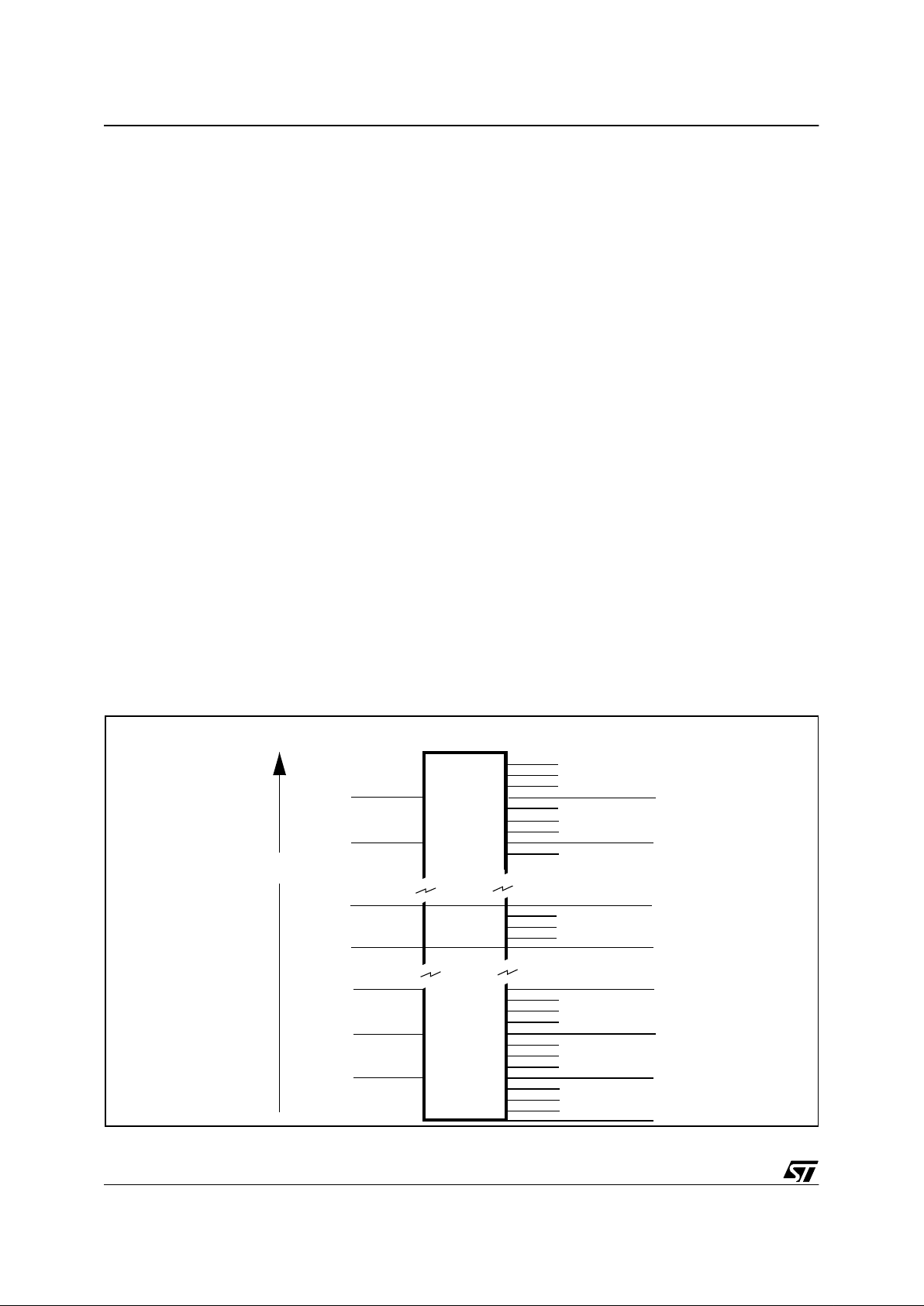
30/398
ST92F124/F150/F250 - DEVICE ARCHITECTURE
2 DEVICE ARCHITECTURE
2.1 CORE ARCHITECTURE
The ST9 Core or Central Processing Unit (CPU)
features a highly optimised instruction set, capable
of handling bit, byte (8-bit) and word (16-bit) data,
as well as BCD and Boolean formats; 14 addressing modes are available.
Four independent buses are controlled by the
Core: a 16-bit Memory bus, an 8-bi t Registe r data
bus, an 8-bit Register ad dress bus an d a 6-bit Interrupt/DMA bus which connect s th e in terrupt an d
DMA controllers in the on-chip peripherals with the
Core.
This multiple bus architecture affords a high degree of pipelining and parallel operation, thus making the ST9 family devices highly efficient, both for
numerical calculation, data handling and with regard to communication with on-chip peripheral resources.
2.2 MEMORY SPACES
There are two separate memory spaces:
– The Register File, which comprises 240 8-bit
registers, arranged as 15 groups (Group 0 to E),
each containing sixteen 8-bit registers plus up to
64 pages of 16 registers mapped in Group F,
which hold data and control bits for the on-chip
peripherals and I/Os.
– A sing le linear memory space acc ommodating
both program and data. All of the physically separate memory areas, including the internal ROM,
internal RAM and ex ternal memory are mapped
in this common address space. The total addressable memory space of 4 Mbytes (limited by
the size of on-chip memory and the number of
external address pins) is arranged as 64 segments of 64 Kbytes. Each segment is further
subdivided into four pages of 16 Kbytes, as illustrated in Figure 18. A Memory Management Unit
uses a set of pointer registers to address a 22-bit
memory field using 16-bit address-based instructions.
2.2.1 Register File
The Register File consists of (see Figure 19):
– 224 general purpose registers (Group 0 to D,
registers R0 to R223)
– 6 system registers in the System Group (Group
E, registers R224 to R239)
– Up to 64 pages, depending on device configura-
tion, each containing up to 16 registers, mapped
to Group F (R240 to R255), see Figure 20.
Figure 18. Sin gl e Pro gram and Data Memory Address Space
3FFFFFh
3F0000h
3EFFFFh
3E0000h
20FFFFh
02FFFFh
020000h
01FFFFh
010000h
00FFFFh
000000h
8
7
6
5
4
3
2
1
0
63
62
2
1
0
Address 16K Pages 64K Segments
up to 4 Mbytes
Data
Code
255
254
253
252
251
250
249
248
247
9
10
11
21FFFFh
210000h
133
134
135
33
Reserved
132
9
 Loading...