

SGS Thomson Microelectronics ST92F120V9, ST92F120V9Q, ST92F120V6Q, ST92F120V1Q, ST92F120R9T Datasheet
...
January 2000 1/320
This ispreliminary information on a new product now in development or undergoing evaluation.Details are subject to change without notice.
Rev. 2.1
ST92F120
8/16-BIT FLASH MCU FAMILY
WITH RAM, EEPROM AND J1850 BLPD
PRELIMINARY DATA
■ Register oriented 8/16 bit CORE with RUN,
WFI, SLOW, HALT and STOP modes
■ 0 - 24 MHz Operation (internal Clock), 4.5 - 5.5
Volt voltage range
■ PLL Clock Generator (3-5 MHz crystal)
■ -40
o
C to 105oC or -40oCto85oC temperature
range
■ Minimum instruction time: 83 ns (24 MHz
internal clock)
■ Internal Memory: Single Voltage FLASH up to
128 Kbytes, RAM 1.5 to 4 Kbytes, EEPROM
512 to 1K bytes
■ 224 general purpose registers (register file)
available as RAM, accumulators or index
pointers
■ TQFP64 or PQFP100 package
■ DMA controller for reduced processor overhead
■ 48 (77 on PQFP100 version) I/O pins
■ 4 external fast interrupts + 1 NMI
■ Up to 16 pins programmable as wake-up or
additional external interrupt with multi-level
interrupt handler
■ 16-bit Timer with 8 bit Prescaler, able to be
used as a Watchdog Timer with a large range of
service time (HW/SW enabling through
dedicated pin)
■ 16-bit Standard Timer that can be used to
generate a time base independent of PLL Clock
Generator
■ Two 16-bit independent Extended Function
Timers (EFTs) with Prescaler, 2 Input Captures
and two Output Compares (PQFP100 only)
■ Two 16-bit Multifunction Timers, with Prescaler,
2 Input Captures and two Output Compares
■ 8-bit Analog to DigitalConverterallowingupto 8
input channelsonTQFP64 or 16 input channels
on PQFP100
■ One or two Serial Communications Interfaces
with asynchronous and synchronous
capabilities. Software Management and
synchronous mode supported
■ Serial Peripheral Interface (SPI) with Selectable
Master/Slave mode
■ J1850 Byte Level Protocol Decoder (JBLPD)
(on some versions only)
■ Full I
2
C multiple Master/Slave Interface
supporting ACCESS BUS
■ Rich InstructionSet with 14 Addressing Modes
■ Division-by-zero trap generation
■ Versatile Development Tools, including
Assembler, Linker, C-Compiler, Archiver,
Source Level Debugger, Hardware Emulators
and Real Time Operating System
DEVICE SUMMARY
Device
J1850
Pack-
age
EFT
I/Os
SCI
Flash RAM E
ST92F120R6T -
TQFP
64
-48
1 36K 1.5K 512
ST92F120JR6T 1
ST92F120V6Q -
PQFP
100
277
ST92F120JV6Q 1
ST92F120R9T -
TQFP
64
-481
60K 2K 512
ST92F120JR9T 1
ST92F120V9Q -
PQFP
100
2772
ST92F120JV9Q 1
ST92F120R1T -
TQFP
64
-481
128K 4K 1K
ST92F120JR1T 1
ST92F120V1Q -
PQFP
100
2772
ST92F120JV1Q 1
PQFP100
TQFP64
9

2/320
Table of Contents
320
9
1 GENERAL DESCRIPTION . . . . . . ................................................ 7
1.1 INTRODUCTION . . . . . . . . . . . . . ............................................ 7
1.1.1 ST9+ Core . . . . . . . . . ................................................7
1.1.2 External Memory Interface . . . . . . . . . . . . . . . . . . . . . . . . . . . . . . . . . . . . . . . . . . . . . 7
1.1.3 On-chip Peripherals . . . . . . ............................................ 7
1.2 PIN DESCRIPTION . . .................................................... 10
1.2.1 Electromagnetic Compatibility (EMC) . .................................. 10
1.2.2 I/O Port Alternate Functions ...........................................10
1.2.3 Termination of Unused Pins ...........................................10
1.2.4 Avoidance of Pin Damage . . . . . . . . . . . . . . . . . ........................... 11
1.3 I/O PORTS . . . . . . . . . . . . . . . . . . ...........................................19
1.4 OPERATING MODES .. . . . ...............................................24
2 DEVICE ARCHITECTURE . . . . . . . . . . ...........................................25
2.1 CORE ARCHITECTURE . . . . . . . . . . . . . . . . . . ................................25
2.2 MEMORY SPACES . . . . . . . . . . . . . . ........................................ 25
2.2.1 Register File . . . . . . . . . . . . . . . . . . . . . . . . . . . . . . . . . . . . . . . . . . . . . . . . . . . . . . . 25
2.2.2 Register Addressing . . . . . . ...........................................27
2.3 SYSTEM REGISTERS . . . . . . . . . . . . . . . . . . . . . . .............................. 28
2.3.1 Central Interrupt Control Register . . . . . ................................. 28
2.3.2 Flag Register . . . . . . . . . . . . . . . . . . . . . . . . . . . . . . . . . . .................... 29
2.3.3 Register Pointing Techniques . . . . . . . . . . . .............................. 30
2.3.4 Paged Registers . . . . ............................................... 33
2.3.5 Mode Register . . . . . . ...............................................33
2.3.6 Stack Pointers . . . . . . . . . . . . . ........................................34
2.4 MEMORY ORGANIZATION . . . . . . . . . . . . . . . ................................. 36
2.5 MEMORY MANAGEMENT UNIT . . . . . . . . . . .................................. 37
2.6 ADDRESS SPACE EXTENSION . . . . . . . . . . . . . . . . . . . . . . . . . . . . . . . . . . . . . . . . . . . . 38
2.6.1 Addressing 16-Kbyte Pages . . . . . . . . . . . . .............................. 38
2.6.2 Addressing 64-Kbyte Segments . . . . . . . . . . . . . . . . . . . . . . . . . . . . ...........39
2.7 MMU REGISTERS . ...................................................... 39
2.7.1 DPR[3:0]: Data Page Registers . . . . . . . . . . . . . . . . . . . . . . . . . . . . . . . . ........ 39
2.7.2 CSR: Code Segment Register . ........................................41
2.7.3 ISR: Interrupt Segment Register . . . . . . ................................. 41
2.7.4 DMASR: DMA Segment Register . . . . . ................................. 41
2.8 MMU USAGE . . . . . . . . . . . . . . . . . . . . . . . . . . ................................. 43
2.8.1 Normal Program Execution . . . . . . . . . . .................................43
2.8.2 Interrupts . . . . . . . . . . . . . . . . . . . . . . . . ................................. 43
2.8.3 DMA . . . . . . . . . . . . . . . . . . ...........................................43
3 SINGLE VOLTAGE FLASH & EEPROM . . . . . . . . .................................. 44
3.1 INTRODUCTION . . . . . . . . . . . . . ...........................................44
3.2 FUNCTIONAL DESCRIPTION . . . . . ......................................... 45
3.2.1 Structure . . . . . . . . . . . . . . . . . . . . . . . . . . . . . . . . . . . . . . . . . . . . . . . . . ........ 45
3.2.2 Software or Hardware EEPROM Emulation (Device dependent option) . ........ 45
3.2.3 Operation . . . . . . . . . . . . . . . . . . . . . . . . . . . . . . ........................... 46
3.3 REGISTER DESCRIPTION . ............................................... 47
3.3.1 Control Registers . . . . . . . . . . . . . . . . . . . . . .............................. 47
3.3.2 Status Registers . . . . . . . . . . . . . . . . . . . . . . . . . ........................... 50
3.4 WRITE OPERATION EXAMPLE . . . . . . . . .................................... 52

3/320
Table of Contents
9
3.5 EEPROM ..............................................................53
3.5.1 Hardware EEPROM Emulation ........................................53
3.5.2 EEPROM Update Operation . . . . . . . . . . . . .............................. 54
3.6 PROTECTION STRATEGY . ...............................................55
3.6.1 Non Volatile Registers . . . . . . . . . . . . . . . . . . . . . . . . . . . . . . . . ............... 55
3.6.2 Temporary Unprotection .. . . . . . . . . . . .................................57
3.7 FLASH IN-SYSTEM PROGRAMMING . . . . . . . ................................57
3.7.1 First Programming of a virgin Flash . . . . . . . . . . . . . . . . . . . . . . ............... 57
4 REGISTER AND MEMORY MAP ................................................ 59
4.1 INTRODUCTION . . . . . . . . . . . . . ...........................................59
4.2 MEMORY CONFIGURATION .. . . . . . . . . . . . ................................. 59
4.3 ST92F120 REGISTERMAP . . . . . . . . . . . . . ..................................62
5 INTERRUPTS . . ............................................................. 72
5.1 INTRODUCTION . . . . . . . . . . . . . ...........................................72
5.2 INTERRUPT VECTORING ................................................ 72
5.2.1 Divide by Zero trap . . . . . . . . . . . . . . . . . ................................. 72
5.2.2 Segment Paging During Interrupt Routines . . . . . . . . . . . .................... 73
5.3 INTERRUPT PRIORITY LEVELS . . . . . . . . . . . . . . . . . . . . . . . . . . . . . . . . . . . . . . . . . . . 73
5.4 PRIORITY LEVEL ARBITRATION . . . ........................................73
5.4.1 Priority level 7 (Lowest) . . . ...........................................73
5.4.2 Maximum depthof nesting . . . . . . . . . . .................................. 73
5.4.3 Simultaneous Interrupts . . . . . . . . . . . . . . . . . . . . . . . . . . . . . . . . . . . . . . . . . . . . . . 73
5.4.4 Dynamic Priority Level Modification . . . . . ................................74
5.5 ARBITRATION MODES . . . . . . . . . . . . . . . . . .................................. 74
5.5.1 Concurrent Mode . . . . . . . . . . . . . . . . . . . . . . . . . . . . . . . . . . . . . . . . . . . . . . . . . . . 74
5.5.2 Nested Mode . . . . . . . . . . . . . . . . . . . . . . . . . . . . . . . . . . .................... 77
5.6 EXTERNAL INTERRUPTS . . . . . . . . . . . . . . . . . . .............................. 79
5.6.1 Standard External Interrupts . . . . . . . . .................................. 79
5.7 TOP LEVEL INTERRUPT . . . . . . . . . . . . . . . . . ................................81
5.8 ON-CHIP PERIPHERAL INTERRUPTS . . . . . . . . . . . . . . . . . . . . . . . . . . . ...........81
5.9 INTERRUPT RESPONSE TIME . ........................................... 82
5.10INTERRUPT REGISTERS . . ...............................................83
5.11WAKE-UP / INTERRUPT LINES MANAGEMENT UNIT (WUIMU) . . . . . . . . . . . . . . . . . . 86
5.11.1Introduction . . . . ...................................................86
5.11.2Main Features . . . . . . . . . . . . . . . . . . . . ................................. 86
5.11.3Functional Description . . . . . . . ........................................ 87
5.11.4Programming Considerations . . . . . . . .................................. 90
5.11.5Register Description . . . . . . . . . ........................................ 91
6 ON-CHIP DIRECT MEMORY ACCESS (DMA) . . . . .................................. 94
6.1 INTRODUCTION . . . . . . . . . . . . . ...........................................94
6.2 DMA PRIORITY LEVELS . . . ...............................................94
6.3 DMA TRANSACTIONS . . . . . . . . . . . ........................................95
6.4 DMA CYCLE TIME . . . . . . . . . . . . . . . ........................................ 97
6.5 SWAP MODE . . . . . . . . . . . . ...............................................97
6.6 DMA REGISTERS . . . . . . . . . . . . ...........................................98

4/320
Table of Contents
320
1
7 RESET AND CLOCK CONTROL UNIT (RCCU) . . . ................................. 99
7.1 INTRODUCTION . . . . . . . . . . . . . ...........................................99
7.2 CLOCK CONTROL UNIT . . . . . . . ........................................... 99
7.2.1 Clock Control Unit Overview . . . . . . . . . . . . . . . ........................... 99
7.3 CLOCK MANAGEMENT . . . . . . . . . . .......................................101
7.3.1 PLL Clock Multiplier Programming . . . . . . . . ............................. 102
7.3.2 CPU Clock Prescaling . . . . . . . . . . . . . .................................102
7.3.3 Peripheral Clock . . . . . . . . . . . . . . . . . . . . . . . . . .......................... 103
7.3.4 Low Power Modes . . . .............................................. 103
7.3.5 Interrupt Generation . . . . . . . . . ....................................... 103
7.4 CLOCK CONTROL REGISTERS . . . . . . . . . . . . . . ............................. 106
7.5 OSCILLATOR CHARACTERISTICS . . . . . . . . . . . .............................109
7.6 RESET/STOP MANAGER . . . . . . .......................................... 111
7.6.1 Reset Pin Timing . . . . ..............................................112
7.7 STOP MODE . . . . . . . . . . . . . . . . . . . .......................................113
8 EXTERNAL MEMORY INTERFACE (EXTMI) . . . . . . . . . . . . . . . . . . . . . . . . . . . . . . . . . . . . . 114
8.1 INTRODUCTION . . . . . . . . . . . . . ..........................................114
8.2 EXTERNAL MEMORY SIGNALS.. . . . . . . . . . . . . . . . .......................... 115
8.2.1 AS: Address Strobe . . .............................................. 115
8.2.2 DS: Data Strobe ................................................... 115
8.2.3 DS2: Data Strobe 2 . . . . . . . . . .......................................115
8.2.4 RW: Read/Write . . . . . . . . . . . . . . . . . . . . . . ............................. 118
8.2.5 BREQ, BACK: Bus Request, Bus Acknowledge . . . . . . . . . . . . . . . . ..........118
8.2.6 PORT 0 . . . . . . . . . . . . . . . .......................................... 119
8.2.7 PORT 1 . . . . . . . . . . . . . . . .......................................... 119
8.2.8 WAIT: External Memory Wait . . . . . . ................................... 119
8.3 REGISTER DESCRIPTION . .............................................. 120
9 I/O PORTS . . . . . . . . . . . . . . . . . . . . . . . . . . .......................................123
9.1 INTRODUCTION . . . . . . . . . . . . . ..........................................123
9.2 SPECIFIC PORT CONFIGURATIONS . . . . . . . . . . . . . . . . . . . . . . . . . . . . . . . ....... 123
9.3 PORT CONTROL REGISTERS . . . . . . . . . . . . . . . . . . .......................... 123
9.4 INPUT/OUTPUT BIT CONFIGURATION . . . . . . . . . . . . . . . . . . . . . . . . . . . . . . . . . . . . . 124
9.5 ALTERNATE FUNCTION ARCHITECTURE . . . . . . . . . . . . . . . . . . . . . . . . ..........128
9.5.1 Pin Declared as I/O . . .............................................. 128
9.5.2 Pin Declared as an Alternate Input . . . . . ...............................128
9.5.3 Pin Declared as an Alternate Function Output . . . . . . . . . . . . . . . . . . . . . ....... 128
9.6 I/O STATUS AFTER WFI, HALT AND RESET . . . . . . . . . . . . . . . . . . . . . . ..........128
10 ON-CHIP PERIPHERALS . . . . . . .............................................. 129
10.1TIMER/WATCHDOG (WDT) . . . . . . . . . . . . . ................................. 129
10.1.1Introduction . . . . ..................................................129
10.1.2Functional Description . . . . . . . .......................................130
10.1.3Watchdog Timer Operation . . . . . . . . . . ................................ 131
10.1.4WDT Interrupts . . . . . . . . . . . . . .......................................133
10.1.5Register Description . . . . . . . . . .......................................134
10.2STANDARD TIMER (STIM) . .............................................. 136
10.2.1Introduction . . . . ..................................................136
10.2.2Functional Description . . . . . . . .......................................137

5/320
Table of Contents
1
10.2.3Interrupt Selection . . . .............................................. 138
10.2.4Register Mapping .. . . . . . . . . . . . . . . . . . . . . . . .......................... 138
10.2.5Register Description . . . . . . . . . .......................................139
10.3EXTENDED FUNCTION TIMER (EFT) . . . . . . ................................ 140
10.3.1Introduction . . . . ..................................................140
10.3.2Main Features . . . . . . . . . . . . . . . . . . . . ................................140
10.3.3Functional Description . . . . . . . .......................................140
10.3.4Interrupt Management . . . . . . . . . . . . . .................................150
10.3.5Register Description . . . . . . . . . .......................................152
10.4MULTIFUNCTION TIMER (MFT) . . . . . . . . . . . . . . . . . . . . . . . . ................... 160
10.4.1Introduction . . . . ..................................................160
10.4.2Functional Description . . . . . . . .......................................162
10.4.3Input Pin Assignment . . . . . ..........................................165
10.4.4Output Pin Assignment . . . . . . ....................................... 169
10.4.5Interrupt and DMA . . . . . . . . . . . . . . . . . . . . . . . . . . . . . . . . . . . . . . . . . . ....... 171
10.4.6Register Description . . . . . . . . . .......................................173
10.5SERIAL COMMUNICATIONS INTERFACE (SCI) . .............................184
10.5.1Introduction . . . . ..................................................184
10.5.2Functional Description . . . . . . . .......................................185
10.5.3SCI Operating Modes . . . . . . . . . . . . . . . . . ............................. 186
10.5.4Serial Frame Format ............................................... 189
10.5.5Clocks And Serial Transmission Rates . . . . ............................. 192
10.5.6SCI Initialization Procedure . . . . . . . . . . . . . . . . . . . . . . . . . . . . . . . . . . . ....... 192
10.5.7Input Signals . . . . . . . . . . . . . . . . . . . . . . . . ............................. 194
10.5.8Output Signals . . . . . . .............................................. 194
10.5.9Interrupts and DMA . . . . . . . . . . . . . . . . . ...............................195
10.5.10Register Description . .............................................. 198
10.6SERIAL PERIPHERAL INTERFACE (SPI) . . . . . . . . . . . . . . . . . . . . . . . . . ..........209
10.6.1Introduction . . . . ..................................................209
10.6.2Main Features . . . . . . . . . . . . . . . . . . . . ................................209
10.6.3General description . . . . . . ..........................................209
10.6.4Functional Description . . . . . . . .......................................211
10.6.5Interrupt Management . . . . . . . . . . . . . .................................218
10.6.6Register Description . . . . . . . . . .......................................219
10.7 I2C BUS INTERFACE . . . . . . . . . . . . . . . . . . ................................. 221
10.7.1Introduction . . . . ..................................................221
10.7.2Main Features . . . . . . . . . . . . . . . . . . . . ................................221
10.7.3Functional Description . . . . . . . .......................................222
10.7.4I2C State Machine . . . . . . . ..........................................224
10.7.5Interrupt Features . . . .............................................. 229
10.7.6DMA Features . . . . . . .............................................. 230
10.7.7Register Description . . . . . . . . . .......................................232
10.8J1850 BYTE LEVEL PROTOCOL DECODER (JBLPD) . . . . . . . . . . . .............. 243
10.8.1Introduction . . . . ..................................................243
10.8.2Main Features . . . . . . . . . . . . . . . . . . . . ................................243
10.8.3Functional Description . . . . . . . .......................................245
10.8.4Peripheral Functional Modes . . ....................................... 256
10.8.5Interrupt Features . . . .............................................. 257
10.8.6DMA Features . . . . . . .............................................. 259

6/320
Table of Contents
320
1
10.8.7Register Description . . . . . . . . . .......................................263
10.9EIGHT-CHANNELANALOG TO DIGITAL CONVERTER (A/D) . . . . . . . . . . . . . . . . . . . 284
10.9.1Introduction . . . . ..................................................284
10.9.2Functional Description . . . . . . . .......................................285
10.9.3Interrupts . . . . . . . . . . . . . . . . . . . . . . . . . ...............................287
10.9.4Register Description . . . . . . . . . .......................................288
11 ELECTRICAL CHARACTERISTICS . . . . ........................................ 292
12 GENERAL INFORMATION ................................................... 319
12.1PACKAGE MECHANICAL DATA . . . . . . . . . . . . . . . . . ..........................319

7/320
ST92F120 - GENERAL DESCRIPTION
1 GENERAL DESCRIPTION
1.1 INTRODUCTION
The ST92F120 microcontroller is developed and
manufactured by STMicroelectronics using a proprietary n-well HCMOS process. Its performance
derives from the use of a flexible256-register programming model for ultra-fast context switching
and real-time event response. The intelligent onchip peripherals offload the ST9 core from I/O and
data management processing tasks allowing critical application tasks to get the maximum use of
core resources. The new-generation ST9 MCU
devices now also support low power consumption
and low voltage operation for power-efficient and
low-cost embedded systems.
1.1.1 ST9+ Core
The advanced Core consists of the Central
Processing Unit(CPU),theRegisterFile, theInterrupt and DMA controller, and the Memory Management Unit. The MMU allows a single linear address space of up to4 Mbytes.
Four independent buses are controlled by the
Core: a 16-bit memory bus, an 8-bit register data
bus, an 8-bit register address bus and a 6-bit interrupt/DMA bus which connects the interrupt and
DMA controllersin the on-chip peripherals with the
core.
This multiple busarchitecture makes the ST9 family deviceshighlyefficient foraccessing onand offchip memory and fast exchange of data with the
on-chip peripherals.
The general-purpose registers can be used as accumulators, index registers, or address pointers.
Adjacent register pairs make up 16-bit registers for
addressing or 16-bit processing. Although the ST9
has an 8-bit ALU, the chip handles 16-bit operations, including arithmetic, loads/stores, and memory/register and memory/memory exchanges.
The powerful I/O capabilities demanded by microcontroller applications are fulfilled by the
ST92F120 with48(TQFP64) or 77 (PQFP100)I/O
lines dedicated to digital Input/Output. These lines
are grouped into up to ten 8-bit I/O Ports and can
be configuredonabit basis under software control
to provide timing, status signals, an address/data
bus for interfacing to the external memory, timer
inputs and outputs, analog inputs, external interrupts and serial or parallel I/O. Two memory spaces are available to support this wide range of configurations: a combined Program/Data Memory
Space and the internal Register File, which includes the control and status registers of the onchip peripherals.
1.1.2 External Memory Interface
PQFP100 devices have a 16-bit external address
bus allowing them to address up to 64K bytes of
external memory. TQFP64 devices have an 11-bit
external address bus for addressing up to 2K
bytes.
1.1.3 On-chip Peripherals
Two 16-bit MultiFunction Timers, each with an 8
bit Prescaler and 12 operating modes allow simple
use for complex waveform generation and measurement, PWM functions and many other system
timing functions by the usage of the two associated DMA channels for each timer.
On PQFP100 devices, two Extended Function
Timers provide further timing and signal generation capabilities.
A Standard Timer can be used to generate a stable time base independent from the PLL.
An I2C interface provides fast I2C and Access Bus
support.
The SPI is a synchronous serial interface for Master and Slave device communication. It supports
single master and multimaster systems.
A J1850 Byte Level Protocol Decoder is available
(on some devices only) for communicating with a
J1850 network.
In addition, there is an16 channel Analog to Digital
Converters with integral sample and hold, fast
conversion time and 8-bit resolution. In the
TQFP64 version only 8 input channels are available.
Completing the device are two or one full duplex
Serial Communications Interfaces with an integral
generator, asynchronous and synchronous capability (fully programmable format) and associated
address/wake-up option, plus two DMA channels.
Finally, a programmable PLL Clock Generator allows the usage of standard 3 to 5 MHz crystals to
obtain a large range of internal frequencies up to
24MHz. Low power Run (SLOW), Wait For Interrupt, low power Wait For Interrupt, STOP and
HALT modes are also available.
9
8/320
ST92F120 - GENERAL DESCRIPTION
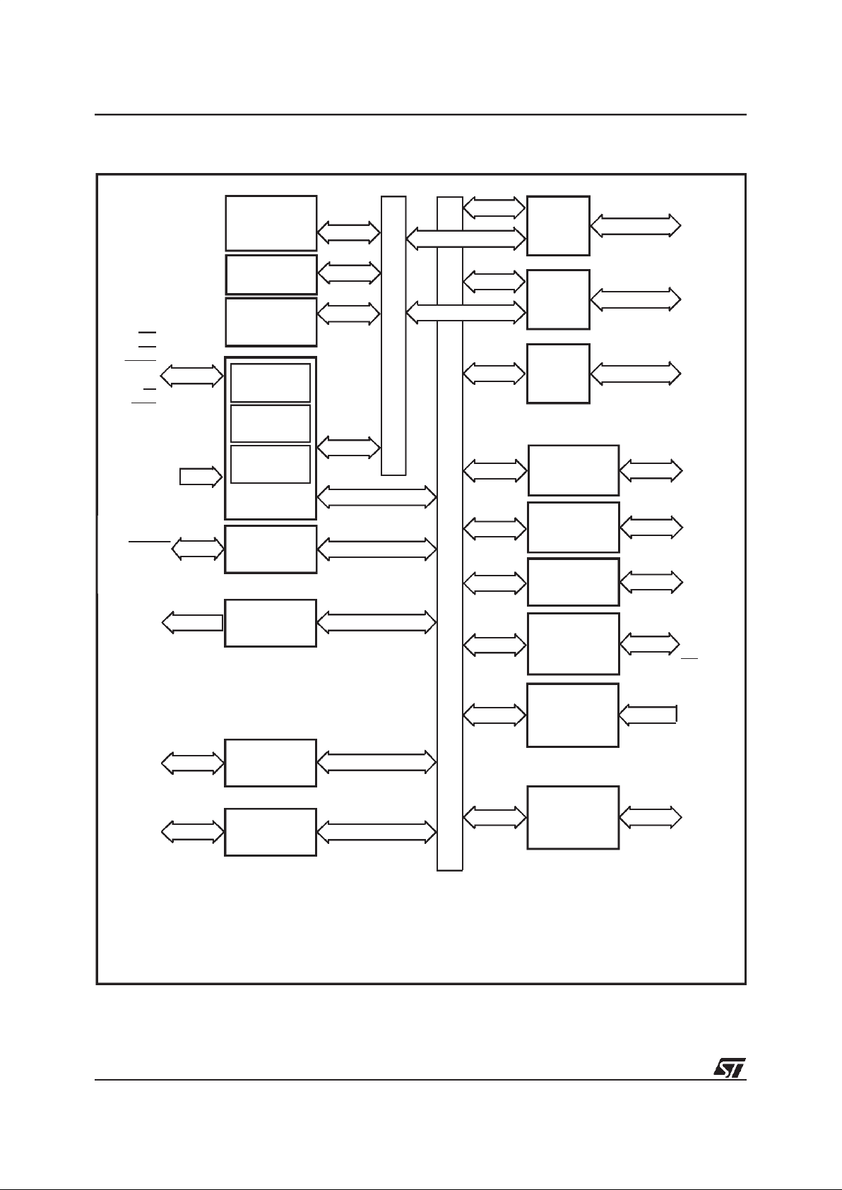
Figure 1. ST92F120JR: Architectural Block Diagram (TQFP64 version)
256 bytes
Register File
RAM
1.5/2/4 Kbytes
ST9 CORE
8/16 bits
CPU
Interrupt
Management
MEMORY BUS
RCCU
Ext.
MEM.
ADDRESS
DATA
Ext. MEM.
AD-
DRESS
REGISTER BUS
WATCHDOG
AS
DS
WAIT
NMI
RW
DS2
MISO
MOSI
SCK
SS
A[10:8]
A[7:0]
D[7:0]
ST. TIMER
SPI
SDAI
SDAO
SCLI
SCLO
I2C BUS
SCI 0
FLASH
36/60/128
Kbytes
TXCLK0
RXCLK0
SIN0
DCD0
SOUT0
CLKOUT0
RTS0
WDOUT
HW0SW1
STOUT
All alternate functions (
Italic characters
) are mapped on Port2, Port3, Port4, Port5, Port6,and Port7
Fully Prog.
I/Os
P0[7:0]
P1[2:0]
P2[7:0]
P3[7:4]
P4[7:4]
P5[7:0]
P6[5:2,0]
P7[7:0]
MF TIMER0
TINPA0
TOUTA0
TINPB0
TOUTB0
TINPA1
TOUTA1
TINPB1
TOUTB1
INT[6:0]
WKUP[15:0]
MF TIMER1
EEPROM
512 /1K bytes
OSCIN
OSCOUT
RESET
CLOCK2/8
INTCLK
A/D CONV. 0
A0IN[7:0]
EXTRG
VPWI
VPWO
J1850
JBLPD
(optional)
9
9/320
ST92F120 - GENERAL DESCRIPTION
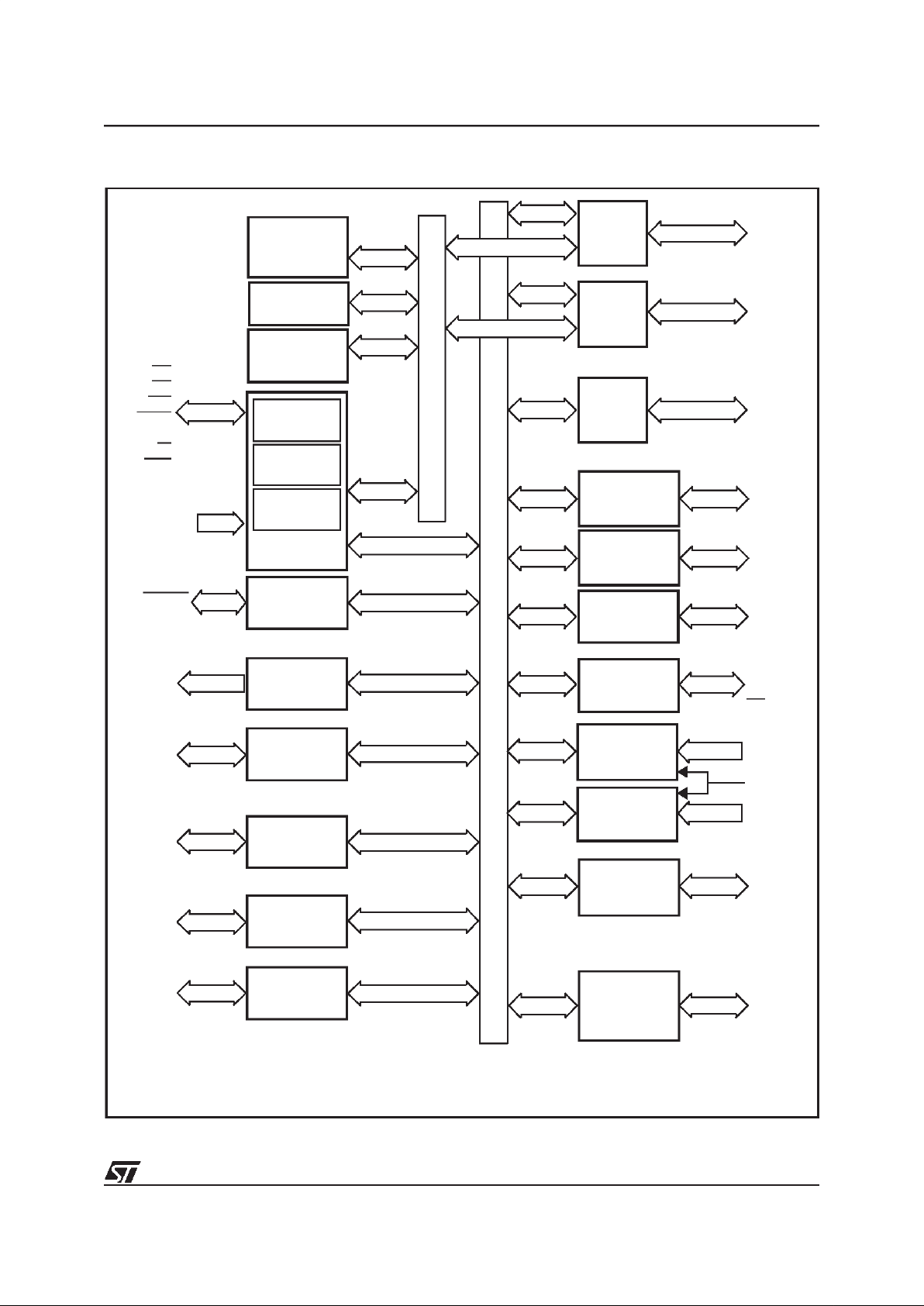
Figure 2. ST92F120JV: Architectural Block Diagram (PQFP100 version)
256 bytes
Register File
ST9 CORE
8/16 bits
CPU
Interrupt
Management
MEMORY BUS
RCCU
REGISTER BUS
WATCHDOG
AS
DS
RW
WAIT
NMI
RW
DS2
MISO
MOSI
SCK
SS
EF TIMER0
ST. TIMER
SPI
SCI 0
TXCLK0
RXCLK0
SIN0
DCD0
SOUT0
CLKOUT0
RTS0
WDOUT
HW0SW1
STOUT
ICAPA0
OCMPA0
ICAPB0
OCMPB0
EXTCLK0
Fully Prog.
I/Os
P0[7:0]
P1[7:0]
P2[7:0]
P3[7:1]
P4[7:0]
P5[7:0]
P6[5:0]
P7[7:0]
P8[7:0]
P9[7:0]
TXCLK1
RXCLK1
SIN1
DCD1
SOUT1
CLKOUT1
RTS1
MF TIMER0
TINPA0
TOUTA0
TINPB0
TOUTB0
ICAPA1
OCMPA1
ICAPB1
OCMPB1
EXTCLK1
TINPA1
TOUTA1
TINPB1
TOUTB1
INT[6:0]
WKUP[15:0]
EF TIMER1
MF TIMER1
SCI 1
*
OSCIN
OSCOUT
RESET
CLOCK2/8
CLOCK2
INTCLK
A/D CONV. 0
A0IN[7:0]
EXTRG
A/D CONV. 1
A1IN[7:0]
SDAI
SDAO
SCLI
SCLO
I2C BUS
VPWI
VPWO
J1850
JBLPD
A[7:0]
D[7:0]
A[15:8]
Ext.
MEM.
ADDRESS
DATA
Ext. MEM.
AD-
DRESS
RAM
1.5/2/4 Kbytes
FLASH
36/60/128
Kbytes
EEPROM
512 /1K bytes
(optional)
All alternate functions (
Italic characters
) are mapped on Port2, Port3,Port4, Port5, Port6, Port7, Port8 and Port9
* Available on some versions only
9

10/320
ST92F120 - GENERAL DESCRIPTION
1.2 PIN DESCRIPTION
AS. Address Strobe (output, active low, 3-state).
Address Strobe is pulsed low once at the beginning of each memory cycle. The rising edge of AS
indicates that address, Read/Write (RW), and
Data signals are valid for memory transfers.
DS. Data Strobe (output, active low, 3-state). Data
Strobe provides the timing for data movement to or
from Port 0 for each memory transfer. During a
write cycle, data out is valid at the leading edge of
DS. During a read cycle, Data In must be valid prior to the trailing edge of DS. When the ST9 accesses on-chip memory, DS is held high during
the whole memory cycle.
RESET. Reset (input, active low). The ST9 is initialised by the Reset signal. With the deactivation
of RESET, program execution begins from the
Program memory location pointed to by the vector
contained in program memory locations 00h and
01h.
RW. Read/Write (output, 3-state). Read/Write determines the direction of data transfer for external
memory transactions. RW is low when writing to
external memory, and high for all other transactions.
OSCIN, OSCOUT. Oscillator (input and output).
These pins connect a parallel-resonant crystal, or
an external source to the on-chip clock oscillator
and buffer. OSCIN is the input of the oscillator inverter and internal clock generator; OSCOUT is
the output of the oscillator inverter.
HW0SW1. When connected to VDDthrough a 1K
pull-up resistor, the software watchdog option is
selected. When connected to VSSthrough a 1K
pull-down resistor, the hardware watchdog option
is selected.
VPWO. This pin is the output line of the J1850 peripheral (JBLPD). It is available only on some devices. On devices without JBLPD peripheral, this
pin must not be connected.
P0[7:0], P1[2:0] or P1[7:0]
(Input/Output, TTL or
CMOS compatible)
. 11 lines (TQFP64 devices) or
16 lines (PQFP100 devices) providing the external
memory interface for addressing 2K or 64 K bytes
of externalmemory.
P0[7:0], P1[2:0], P2[7:0], P3[7:4], P4.[7:4],
P5[7:0], P6[5:2,0], P7[7:0]
I/O Port Lines (Input/
Output, TTL or CMOS compatible)
. I/O lines
grouped into I/O ports of 8 bits, bit programmable
under software control as general purpose I/O or
as alternate functions.
P1[7:3], P3[3:1], P4[3:0], P6.1, P8[7:0], P9[7:0]
Additional I/O Port Lines available on PQFP100
versions only.
AVDD. Analog VDDof the Analog to Digital Con-
verter (common for A/D 0 and A/D 1).
AVSS. Analog VSSof the Analog to Digital Con-
verter (common for A/D 0 and A/D 1).
VDD. Main Power Supply Voltage. Four pins are
available on PQFP100 versions, two on TQFP64
versions. The pins are internally connected.
VSS. Digital Circuit Ground. Four pins are available on PQFP100 versions, two on TQFP64 versions. The pins are internally connected.
VPP. Power Supply Voltage for Flash test purposes. This pin is bonded and must be kept to 0 in
user mode.
V
REG
. 3V regulator output.
1.2.1 Electromagnetic Compatibility (EMC)
To reduce the electromagnetic interference thefollowing features have been implemented:
– A low power oscillator is included with a control-
led gain to reduce EMI and the power consumption in Halt mode.
– Two or Four pairs of digital power supply pins
(VDD,VSS) are located on each side of the
PQFP100 package (2 pairs on TQFP64).
– Digital and analog power supplies are complete-
ly separated.
– Digital power supplies for internal logic and I/O
ports are separated internally.
– Internal decoupling capacitance is located be-
tween VDDand VSS.
Note: Each pair of digital VDD/VSSpins should be
externally connected by a 10 µF chemical pulling
capacitor and a 100 nF ceramic chip capacitor.
1.2.2 I/O Port Alternate Functions
Each pin of the I/O ports of the ST92F120 may assume software programmable Alternate Functions
as shown in Section 1.3.
1.2.3 Termination of Unused Pins
The ST9 deviceis implemented using CMOS technology; therefore unused pins must be properly
terminated in order to avoid application reliability
problems. In fact, as shown in Figure 3, the standard input circuitry is based on the CMOS inverter
structure.
9
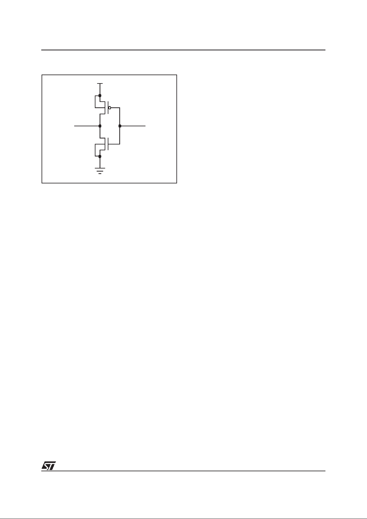
11/320
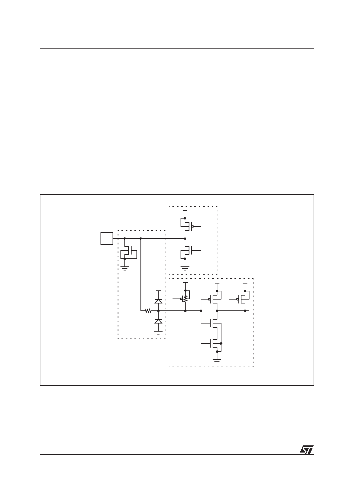
ST92F120 - GENERAL DESCRIPTION
Figure 3. CMOS basic inverter
When an input is kept at logic zero, the N-channel
transistor is off, while the P-channel is on and can
conduct. The opposite occurs when an input is
kept at logic one. CMOS transistors are essentially
linear devices with relatively broad switching
points. During commutation, the input passes
through midsupply, and there is a region of input
voltage values where both P and N-channel transistors are on. Since normally the transitions are
fast, there is a very short time in which a current
can flow: once the switching is completed there is
no longer current. This phenomenon explains why
the overall current depends on the switching rate:
the consumption is directly proportional to the
number of transistors inside the device which are
in the linear region during transitions, charging and
discharging internal capacitances.
In order to avoid extra power supply current, it is
important to bias input pins properly when not
used. In fact, if the input impedance is very high,
pins can float, when not connected, either to a
midsupply level or can oscillate (injecting noise in
the device).
Depending on the specific configuration of each
I/O pin on different ST9 devices, it can be more or
less critical to leave unused pins floating. For this
reason, on most pins, the configuration after RESET enables an internal weak pull-up transistor in
order to avoid floating conditions. For other pins
this is intrinsically forbidden, like for the true opendrain pins. In any case, the application software
must program the right state for unused pins to
avoid conflicts with external circuitry (whichever it
is: pull-up, pull-down, floating, etc.).
The suggested method of terminating unused I/O
is to connect an external individual pull-up or pulldown for each pin, even though initialization software can force outputs to a specified and defined
value, during a particular phaseof the RESET routine there could be an undetermined status at the
input section.
Usage of pull-ups and/or pull-downs is preferable
in place of direct connection to VDDor VSS. If pullup or pull-down resistors are used, inputs can be
forced for test purposes to a different value, and
outputs can be programmed to both digital levels
without generating high current drain due to the
conflict.
Anyway, during system verification flow, attention
must be paid to reviewing the connection of each
pin, in order to avoid potential problems.
1.2.4 Avoidance of Pin Damage
Although integrated circuit data sheets provide the
user with conservative limits and conditions in order to prevent damage, sometimes it is useful for
the hardware system designer to know the internal
failure mechanisms: the risk of exposure to illegal
voltages and conditions can be reduced by smart
protection design.
It is not possible to classify and to predict all the
possible damage resulting from violating maximum ratings and conditions, due to the large
number of variables that come into play in defining
the failures: in fact, when an overvoltage condition
is applied, the effects on the device can vary significantly depending on lot-to-lot process variations, operating temperature, external interfacing
of the ST9 with other devices, etc.
In the following sections, background technical information is given in order to help system designers to reduce risk of damage to the ST9 device.
1.2.4.1 Electrostatic Discharge and Latchup
CMOS integrated circuits are generally sensitive
to exposure to highvoltage static electricity, which
can induce permanent damage to the device: a
typical failure is the breakdown of thin oxides,
which causeshigh leakage current and sometimes
shorts.
Latchup is another typical phenomenon occurring
in integrated circuits: unwanted turning on of parasitic bipolar structures, or silicon-controlled rectifiers (SCR), may overheat and rapidly destroy the
device. These unintentional structures are composed of P and N regions which work as emitters,
bases and collectors of parasitic bipolar transistors: the bulk resistance of the silicon in the wells
and substrate act as resistors on the SCR structure. Applying voltages below VSSor above VDD,
and when the level of current is able to generatea
P
N
INOUT
V
DD
V
SS
1
12/320
ST92F120 - GENERAL DESCRIPTION
voltage drop across the SCR parasitic resistor, the
SCR may be turned on; to turn off the SCR it is
necessary to remove the power supply from the
device.
The present ST9 design implements layout and
process solutions to decrease the effects of electrostatic discharges (ESD) and latchup. Of course
it is not possible to test all devices, due to the destructive nature of the mechanism; in order to
guarantee product reliability, destructive tests are
carried out on groups of devices, according to
STMicroelectronics internal Quality Assurance
standards and recommendations.
1.2.4.2 Protective Interface
Although ST9 input/output circuitry has been designed taking ESD and Latchup problems into ac-
count, for those applications and systems where
ST9 pins are exposed to illegal voltages and high
current injections, the user is strongly recommended to implement hardware solutions which reduce
the risk ofdamage to the microcontroller: low-pass
filters and clamp diodes are usually sufficient in
preventing stress conditions.
The risk of having out-of-range voltages and currents is greater for those signals coming from outside the system, where noise effect or uncontrolled spikes could occur with higher probability
than for the internal signals; it must be underlined
that in somecases, adoption of filters or other dedicated interface circuitries might affect global microcontroller performance, inducingundesired timing delays, and impacting the global system
speed.
Figure 4. Digital Input/Output - Push-Pull
PIN
OUTPUT
BUFFER
P
N
P
N
N
INPUT
BUFFER
P
ESDPR O TE CT ION
CIRCUITRY
PORTCIRCUITRY
I/O CIRCUITRY
P
EN
EN
1
13/320
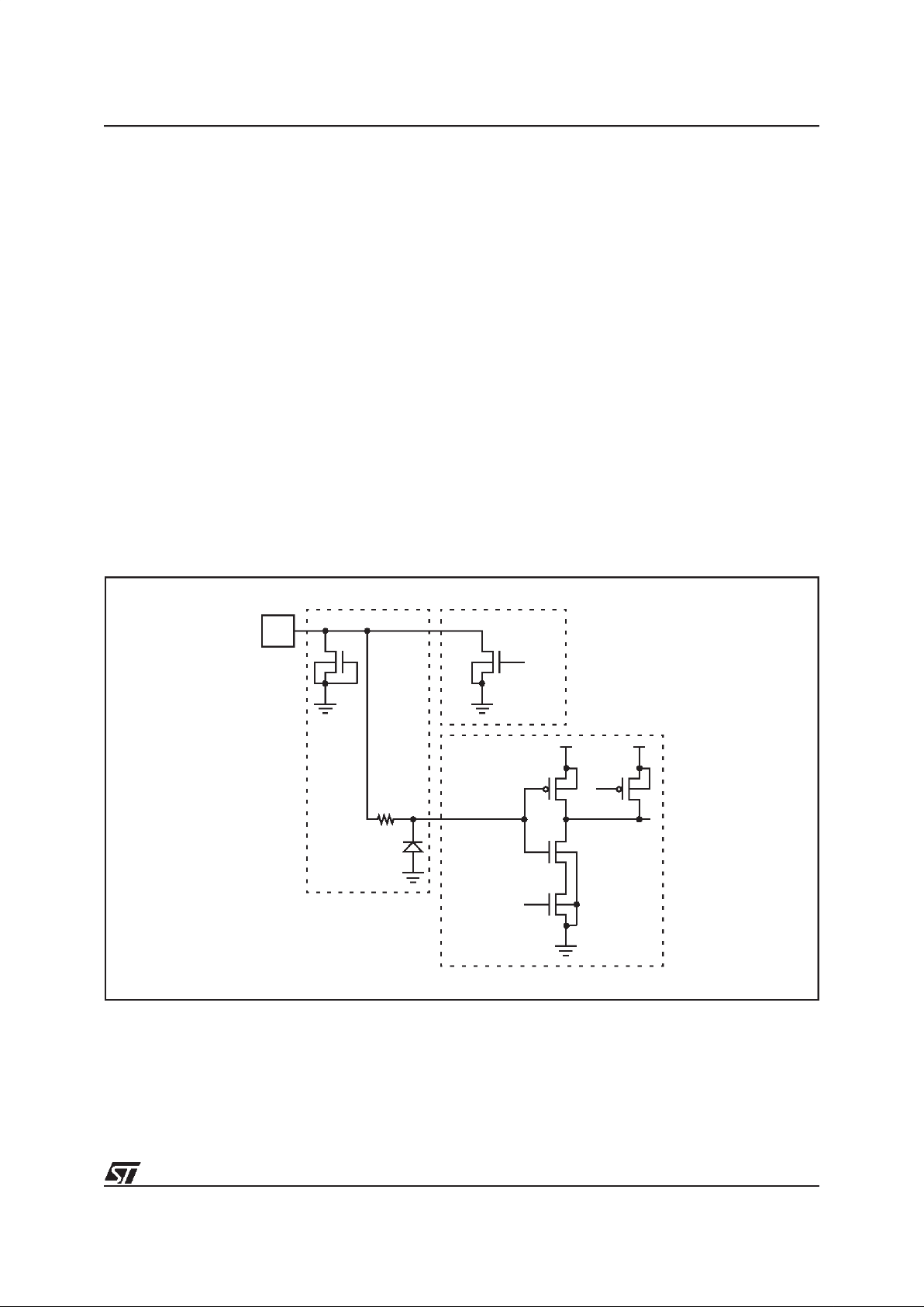
ST92F120 - GENERAL DESCRIPTION
1.2.4.3 Internal Circuitry: Digital I/O pin
In Figure 4a schematic representation of an ST9
pin able to operate either as an input or as an output is shown. The circuitry implements a standard
input buffer and a push-pull configuration for the
output buffer. It is evident that although it is possible to disable the output buffer when the input section is used, the MOS transistors of the buffer itself
can still affect the behaviour of the pin when exposed to illegal conditions. In fact, the P-channel
transistor of the output buffer implements a direct
diode toVDD(P-diffusionof the drain connected to
the pin and N-well connected to VDD), while the Nchannel of the output buffer implements a diode to
VSS(P-substrate connected to VSS and N-diffusion of the drain connected to the pin). In parallel
to these diodes, dedicated circuitry is implemented
to protect the logic from ESD events (MOS, diodes
and input series resistor).
The most important characteristic of these extra
devices is that they must not disturb normal operating modes, while acting during exposure to over
limit conditions, avoiding permanent damage to
the logic circuitry.
All I/O pins can generally be programmed to work
also as open-drain outputs, by simply writing in the
corresponding register of the I/O Port. The gate of
the P-channel of the output buffer is disabled: it is
important tohighlight that physically the P-channel
transistor is still present, so the diode to V
DD
works. In some applications it can occur that the
voltage applied to the pin is higher than the V
DD
value (supposing the external line is kept high,
while the ST9 power supply is turned off): this condition will inject current through the diode, risking
permanent damages to the device.
In any case, programming I/O pins as open-drain
can help when several pins in the system are tied
to the same point: of course software must pay attention to program only one of them as output at
any time, to avoid output driver contentions; it is
advisable to configure these pins as output opendrain in order to reduce the risk of current contentions.
Figure 5. Digital Input/Output - True Open Drain Output
PIN
OUTPUT
BUFFER
N
P
N
N
INPUT
BUFFE R
ESDPROT EC T ION
CIRCUITRY
PORT CIRCUITRY
I/OCIRCUITRY
P
EN
EN
9
14/320
ST92F120 - GENERAL DESCRIPTION
In Figure 6 a true open-drain pin schematic is
shown. In this case all paths to VDDare removed
(P-channel driver, ESD protection diode, internal
weak pull-up) in order to allow the system to turn
off the power supply of the microcontroller and
keep the voltage level at the pin high without injecting current in the device. This is a typical condition which can occur when several devices interface a serial bus: if one device is not involved in
the communication, it can be disabled by turning
off its power supply to reduce the system current
consumption.
When an illegal negative voltage level is applied to
the ST9 I/O pins (both versions, push-pull and true
open-drain output) the clamp diode is always
present and active (see ESD protection circuitry
and N-channel driver).
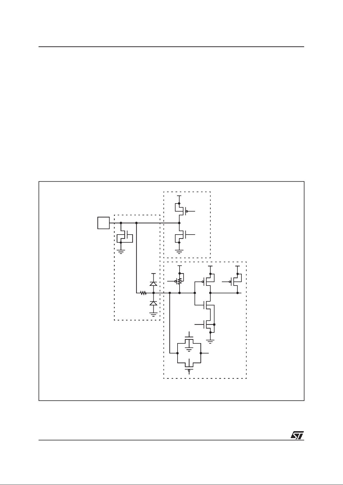
1.2.4.4 Internal Circuitry: Analog Input pin
Figure 6 shows the internal circuitry used for analog input. It is substantially a digital I/O with an
added analog multiplexer for the A/D Converter input signal selection.
The presence of the multiplexer P-channel and Nchannel can affect the behaviour of the pin when
exposed to illegal voltage conditions. These transistors are controlled by a low noise logic, biased
through AVDDand AVSSincluding P-channel Nwell: it is important to always verify the input voltage value with respect to both analog power supply and digital power supply, in order to avoid unintended current injections which (if not limited)
could destroy the device.
Figure 6. Digital Input/Output - Push-Pull Output - Analog Multiplexer Input
PIN
OUTPUT
BUFFER
P
N
P
N
N
IN P UT
BUFFER
P
ESDPRO T EC T ION
CIRCUITRY
PORTCIR CUIT RY
I/OCIRCUITRY
P
EN
EN
N
P
AV
DD
9
15/320
ST92F120 - GENERAL DESCRIPTION
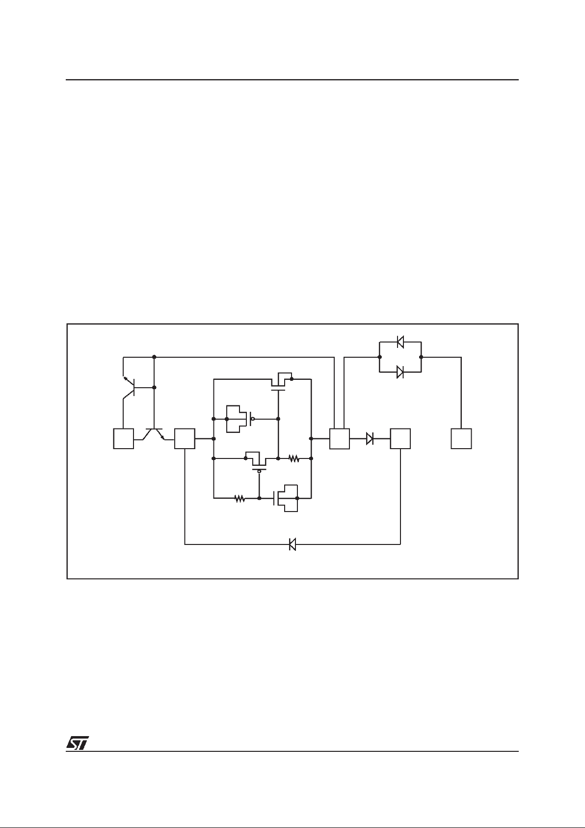
1.2.4.5 Power Supply and Ground
As already said for the I/O pins, in order to guarantee ST9 compliancy with respect to QualityAssurance recommendations concerning ESD and
Latchup, dedicated circuits are added to the different power supply and ground pins (digital and analog). These structures create preferred paths for
the high current injected during discharges, avoiding damage to active logic and circuitry. It is important for the system designer to take this added circuitry into account, which is not always transparent withrespect to the relative level of voltages applied to the different power supply and ground
pins. Figure 7 shows schematically the protection
net implemented on ST9 devices, composedof diodes and other special structures.
The clamp structure between the VDDand V
SS
pins is designed to be active during very fast tran-
sitions (typical of electrostatic discharges). Other
paths are implemented through diodes: they limit
the possibility of positively differentiating AV
DD
and VDD(i.e. AVDD>VDD); similar considerations
are valid for AVSSand VSSdue to the back-toback diode structure implemented between the
two pins. Anyway, it must be highlighted that, because VSSand AVSSare connected to the substrate of the silicon die (even though in different areas of the die itself), they represent the reference
point from which all other voltages are measured,
and it is recommended to never differentiate AV
SS
from VSS.
Note: If more than one pair of pins for VSSand
VDDisavailable on the device, they are connected
internally and the protection net diagram remains
the same as shown in Figure 7.
Figure 7. Power Supplyand Ground configuration
N
P
P
N
V
DD
V
SS
AV
DD
AV
SS
V
PP
9
16/320
ST92F120 - GENERAL DESCRIPTION
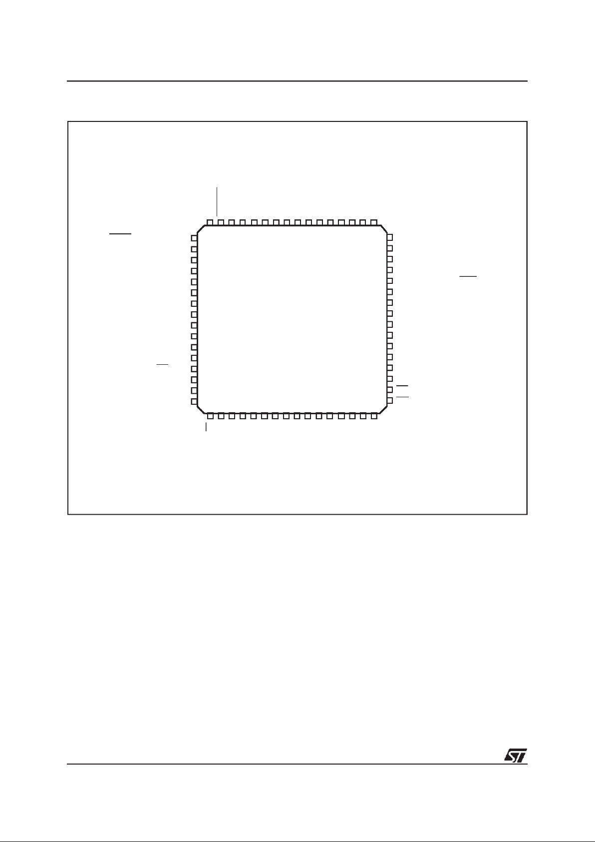
Figure 8. ST92F120: Pin configuration (top-view TQFP64)
* Alternate function forCAN interface, reserved for future use: P5.0/TXCAN0; P5.1/RXCAN0.
** On devices without JBPLD peripheral, this pin must notbe connected.
*** V
PP
must be keptlow in standard operating mode.
WAIT/WKUP5/P5.0*
WKUP6/WDOUT/P5.1*
SIN0/WKUP2/P5.2
SOUT0/P5.3
TXCLK0/CLKOUT0/P5.4
RXCLK0/WKUP7/P5.5
DCD0/WKUP8/P5.6
WKUP9/RTS0/P5.7
EXTCLK1/WKUP4/P4.4
EXTRG/STOUT/P4.5
SDA/P4.6
WKUP1/SCL/P4.7
EXTCLK0/SS/P3.4
MISO/P3.5
MOSI/P3.6
SCK/WKUP0/P3.7
HW0SW1
RESET
OSCOUT
OSCIN
VDDVSSP7.7/A0IN7/WKUP13
P7.6/A0IN6/WKUP12
P7.5/A0IN5/WKUP11
P7.4/A0IN4/WKUP3
P7.3/A0IN3
P7.2/A0IN2
P7.1/A0IN1
P7.0/A0IN0
AVSSAV
DD
VPWO**
P6.5/WKUP10/INTCLK/VPWI
P6.4/NMI
P6.3/INT3/INT5
P6.2/INT2/INT4/DS2
P6.0/INT0/INT1/CLOCK2/8
P0.7/A7/D7
P0.6/A6/D6
P0.5/A5/D5
P0.4/A4/D4
P0.3/A3/D3
P0.2/A2/D2
P0.1/A1/D1
P0.0/A0/D0
AS
DS
RW
TINPA0/P2.0
TINPB0/P2.1
TOUTA0/P2.2
TOUTB0/P2.3
TINPA1/P2.4
TINPB1/P2.5
TOUTA1/P2.6
TOUTB1/P2.7
V
SS
V
DD
V
REG
***V
PP
A8/P1.0
A9/P1.1
A10/P1.2
N.C. = Not connected (no physical bonding wire)
6463 6261 6059585756555453 52515049
48
47
46
45
44
43
42
41
40
39
38
37
36
35
34
33
1718192021222324 29 30313225262728
1
2
3
4
5
6
7
8
9
10
11
12
13
14
15
16
ST92 F12 0
9
17/320
ST92F120 - GENERAL DESCRIPTION
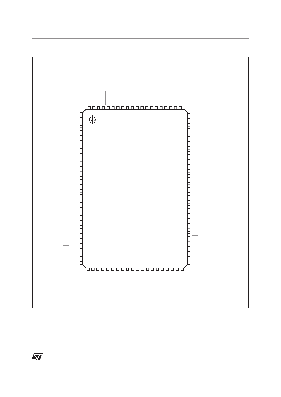
Figure 9. ST92F120: Pin Configuration (top-view PQFP100)
* Alternate function forCAN interface, reserved for future use: P5.0/TXCAN0; P5.1/RXCAN0
** Pin reserved forfuture use: 49- RXCAN1; 50 -TXCAN1
*** V
PP
must be kept low in standard operating mode.
RXCLK1/P9.3
DCD1/P9.4
RTS1/P9.5
CLOCK2/P9.6
P9.7
WAIT/WKUP5/P5.0*
WKUP6/WDOUT/P5.1*
SIN0/WKUP2/P5.2
SOUT0/P5.3
TXCLK0/CLKOUT0/P5.4
RXCLK0/WKUP7/P5.5
DCD0/WKUP8/P5.6
WKUP9/RTS0/P5.7
ICAPA1/P4.0
P4.1
OCMPA1/P4.2
V
SS
V
DD
ICAPB1/OCMPB1/P4.3
EXTCLK1/WKUP4/P4.4
EXTRG/STOUT/P4.5
SDA/P4.6
WKUP1/SCL/P4.7
ICAPB0/P3.1
ICAPA0/OCMPA0/P3.2
OCMPB0/P3.3
EXTCLK0/SS/P3.4
MISO/P3.5
MOSI/P3.6
SCK/WKUP0/P3.7
P9.2/TXCLK1/CLKOUT1
P9.1/SOUT1
P9.0/SIN1
HW0SW1
RESET
OSCOUT
OSCIN
VDDVSSP7.7/A0IN7/WKUP13
P7.6/A0IN6/WKUP12
P7.5/A0IN5/WKUP11
P7.4/A0IN4/WKUP3
P7.3/A0IN3
P7.2/A0IN2
P7.1/A0IN1
P7.0/A0IN0
AVSSAVDDP8.7/A1IN0
P8.6/A1IN1
P8.5/A1IN2
P8.4/A1IN3
P8.3/A1IN4
P8.2/A1IN5
P8.1/A1IN6/WKUP15
P8.0/A1IN7/WKUP14
VPWO
P6.5/WKUP10/INTCLK/VPWI
P6.4/NMI
P6.3/INT3/INT5
P6.2/INT2/INT4/DS2
P6.1/INT6/RW
P6.0/INT0/INT1/CLOCK2/8
P0.7/A7/D7
V
DD
V
SS
P0.6/A6/D6
P0.5/A5/D5
P0.4/A4/D4
P0.3/A3/D3
P0.2/A2/D2
P0.1/A1/D1
P0.0/A0/D0
AS
DS
P1.7/A15
P1.6/A14
P1.5/A13
P1.4/A12
V
REG
RW
TINPA0/P2.0
TINPB0/P2.1
TOUTA0/P2.2
TOUTB0/P2.3
TINPA1/P2.4
TINPB1/P2.5
TOUTA1/P2.6
TOUTB1/P2.7
V
SS
V
DD
V
REG
***V
PP
A8/P1.0
A9/P1.1
A10/P1.2
A11/P1.3
**N.C.
**N.C.
1
50
30
ST92F120
N.C. = Not connected (no physical bonding wire)
2
3
4
5
6
7
8
9
10
11
12
13
14
15
16
17
18
19
20
21
22
23
24
25
26
27
28
29
80
51
79
78
77
76
75
74
73
72
71
70
69
68
67
66
65
64
63
62
61
60
59
58
57
56
55
54
53
52
49484746454443424140393837363534333231
81828384858687888990919293949596979899100
9
18/320
ST92F120 - GENERAL DESCRIPTION
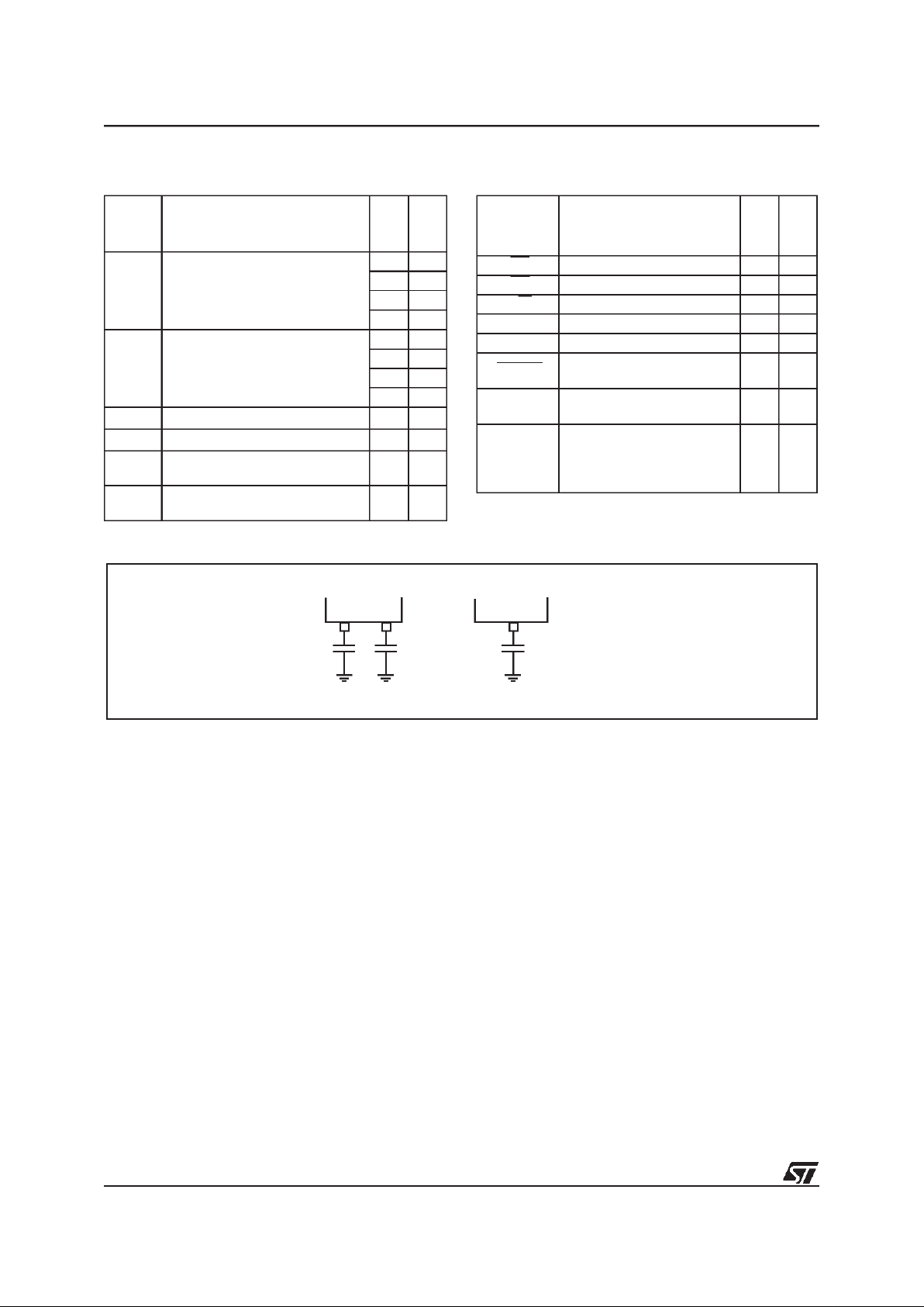
Table 1. ST92F120 Power Supply Pins Table 2. ST92F120 Primary Function Pins
Figure 10. Recommended connections for V
REG
Note : For future compatibility with shrinked versions, the V
REG
pins should be connected to a minimum
of 600 nF (total). Special care should be taken to minimize the distance between the ST9 microcontroller
and the capacitors.
Name Function
QFP64
QFP100
V
DD
Main Power Supply Voltage
( pins internally connected)
-18
27 42
-65
60 93
V
SS
Digital Circuit Ground
(pins internally connected)
-17
26 41
-64
59 92
AV
DD
Analog Circuit Supply Voltage 49 82
AV
SS
Analog Circuit Ground 50 83
V
PP
Must be kept low in standard
operating mode
29 44
V
REG
3V regulator output 28
31
43
Name Function
QFP64
QFP100
AS Address Strobe 34 56
DS Data Strobe 33 55
RW Read/Write 17 32
OSCIN Oscillator Input 61 94
OSCOUT Oscillator Output 62 95
RESET
Reset to initialize theMicro-
controller
63 96
HW0SW1
Watchdog HW/SW enabling
selection
64 97
VPWO
J1850 JBLPD Output. On
devices without JBPLD pe-
ripheral, this pin must not be
connected.
48 73
300 nF 300 nF
QFP100 QFP 64
600 nF
9
19/320
ST92F120 - GENERAL DESCRIPTION
1.3 I/O PORTS
Port 0 and Port 1 provide theexternal memory interface. All the ports of the device can be programmed as Input/Output or in Input mode, compatible with TTL or CMOS levels (except where
Schmitt Trigger is present). Each bit can be programmed individually (Refer to the I/O ports chapter).
Internal Weak Pull-up
As shown in Table 3, not all input sections implement a Weak Pull-up. This means that the pull-up
must be connected externally when the pin is not
used or programmed as bidirectional.
TTL/CMOS Input
For all those port bits where no input schmitt trigger is implemented, it is always possible to program the input level as TTL or CMOS compatible
by programming the relevant PxC2.n control bit.
Refer I/O Ports Chapter to the section titled “Input/
Output Bit Configuration”.
Schmitt Trigger Input
Two different kind ofSchmitt Trigger circuitries are
implemented: Standard and High Hysteresis.
Standard Schmitt Trigger is widely used (see Table 3), while the High Hysteresis one is present on
the NMI and VPWI input function pins mapped on
Port 6 [5:4] (see Table 4).
All inputs which can be used for detecting interrupt
events have been configured with a “standard”
Schmitt Trigger, apart from, as already said, the
NMI pin which implements the “High Hysteresis”
version. In this way, all interrupt lines are guaranteed as “level sensitive”.
Push-Pull/OD Output
The output buffer can be programmed as pushpull or open-drain: attention must be paid to the
fact that the open-drain option corresponds only to
a disabling of P-channel MOS transistor of the
buffer itself: it is still present and physically connected to thepin. Consequentlyit is notpossible to
increase the output voltage on the pin over
VDD+0.3 Volt, to avoid direct junction biasing.
Pure Open-drain Output
The user can increase the voltage on an I/O pin
over VDD+0.3 Volt where the P-channel MOS transistor is physically absent: this is allowed on all
“Pure Open Drain” pins. Of course, in this case the
push-pull option is not available and any weak
pull-up must implemented externally.
Table 3. I/O Port Characteristics
Legend: WPU = Weak Pull-Up, OD = Open Drain
Input Output Weak Pull-Up Reset State
Port 0[7:0] TTL/CMOS Push-Pull/OD No Bidirectional
Port 1[7:0] TTL/CMOS Push-Pull/OD No Bidirectional
Port 2[1:0]
Port 2[3:2]
Port 2[5:4]
Port 2[7:6]
Schmitt trigger
TTL/CMOS
Schmitt trigger
TTL/CMOS
Push-Pull/OD
Pure OD
Push-Pull/OD
Push-Pull/OD
Yes
No
Yes
Yes
Input
Input CMOS
Input
Input CMOS
Port 3[2:1]
Port 3.3
Port 3[7:4]
Schmitt trigger
TTL/CMOS
Schmitt trigger
Push-Pull/OD
Push-Pull/OD
Push-Pull/OD
Yes
Yes
Yes
Input
Input CMOS
Input
Port 4.0, Port 4.4
Port 4.1
Port 4.2, Port 4.5
Port 4.3
Port 4[7:6]
Schmitt trigger
TTL/CMOS
TTL/CMOS
Schmitt trigger
Schmitt trigger inside I/O cell
Push-Pull/OD
Push-Pull/OD
Push-Pull/OD
Push-Pull/OD
Pure OD
No
Yes
Yes
Yes
No
Input
Bidirectional WPU
Input CMOS
Input
Input
Port 5[2:0], Port [7:4]
Port 5.3
Schmitt trigger
TTL/CMOS
Push-Pull/OD
Push-Pull/OD
No
Yes
Input
Input CMOS
Port 6[3:0]
Port 6[5:4]
Schmitt trigger
High hysteresis Schmitt trigger
inside I/O cell
Push-Pull/OD
Push-Pull/OD
Yes
Yes (inside I/O cell)
Input
Input
Port 7[7:0] Schmitt trigger Push-Pull/OD Yes Input
Port 8[1:0]
Port 8[7:2]
Schmitt trigger
Schmitt trigger
Push-Pull/OD
Push-Pull/OD
Yes
Yes
Input
Bidirectional WPU
Port 9[7:0] Schmitt trigger Push-Pull/OD Yes Bidirectional WPU
9

20/320
ST92F120 - GENERAL DESCRIPTION
How to Configure the I/O ports
To configure the I/O ports, use the information in
Table 3, Table 4 andthe Port Bit Configuration Table in the I/O Ports Chapter (See page 125).
Input Note = the hardware characteristics fixed for
each port line in Table3.
– If Input note = TTL/CMOS, either TTL or CMOS
input level can be selected by software.
– If Input note = Schmitt trigger, selecting CMOS
or TTL input by software has no effect, the input
will always be Schmitt Trigger.
Alternate Functions (AF) = More than one AF
cannot beassigned to an I/O pin at the same time:
An alternate function can be selected as follows.
AF Inputs:
– AF is selected implicitly by enabling the corre-
sponding peripheral. Exception to this areA/Dinputs which must be explicitly selected as AF by
software.
AF Outputs or Bidirectional Lines:
– In the case of Outputs or I/Os, AF is selected ex-
plicitly by software.
Example 1: SCI input
AF: SIN0, Port: P5.2, Input note: Schmitt Trigger.
Write the port configuration bits:
P5C2.2=1
P5C1.2=0
P5C0.2 =1
Enable the SCI peripheral by software as described in the SCI chapter.
Example 2: SCI output
AF: SOUT0, Port: P5.3, Output note:
Push-Pull/OD.
Write the port configuration bits (for AF OUT PP):
P5C2.3=0
P5C1.3=1
P5C0.3 =1
Example 3: External Memory I/O
AF: A0/D0, Port : P0.0, Input Note: TTL/CMOS
Write the port configuration bits:
P0C2.0=1
P0C1.0=1
P0C0.0 =1
Example 4: Analog input
AF: A0IN0, Port : 7.0, Input Note: does not apply
to analog input
Write the port configuration bits:
P7C2.0=1
P7C1.0=1
P7C0.0 =1
9
21/320
ST92F120 - GENERAL DESCRIPTION
Table 4. I/O Port Alternate Functions
Port
Name
General
Purpose I/O
Pin No.
Alternate Functions
TQFP64 PQFP100
P0.0
All ports useable
for general purpose I/O (input,
output or bidirectional)
35 57 A0/D0 I/O Address/Data bit 0
P0.1 36 58 A1/D1 I/O Address/Data bit 1
P0.2 37 59 A2/D2 I/O Address/Data bit 2
P0.3 38 60 A3/D3 I/O Address/Data bit 3
P0.4 39 61 A4/D4 I/O Address/Data bit 4
P0.5 40 62 A5/D5 I/O Address/Data bit 5
P0.6 41 63 A6/D6 I/O Address/Data bit 6
P0.7 42 66 A7/D7 I/O Address/Data bit 7
P1.0 30 45 A8 I/O Address bit 8
P1.1 31 46 A9 I/O Address bit 9
P1.2 32 47 A10 I/O Address bit 10
P1.3 - 48 A11 I/O Address bit 11
P1.4 - 51 A12 I/O Address bit 12
P1.5 - 52 A13 I/O Address bit 13
P1.6 - 53 A14 I/O Address bit 14
P1.7 - 54 A15 I/O Address bit 15
P2.0 18 33 TINPA0 I Multifunction Timer 0 - Input A
P2.1 19 34 TINPB0 I Multifunction Timer 0 - Input B
P2.2 20 35 TOUTA0 O Multifunction Timer 0 - Output A
P2.3 21 36 TOUTB0 O Multifunction Timer 0 - Output B
P2.4 22 37 TINPA1 I Multifunction Timer 1 - Input A
P2.5 23 38 TINPB1 I Multifunction Timer 1 - Input B
P2.6 24 39 TOUTA1 O Multifunction Timer 1 - Output A
P2.7 25 40 TOUTB1 O Multifunction Timer 1 - Output B
P3.1 - 24 ICAPB0 I Ext. Timer 0 - Input Capture B
P3.2 - 25
ICAPA0 I Ext. Timer0 - Input Capture A
OCMPA0 O Ext. Timer0 - Output Compare A
P3.3 - 26 OCMPB0 O Ext. Timer 0 - Output Compare B
P3.4 13 27
EXTCLK0 I Ext. Timer 0 - Input Clock
SS I SPI - Slave Select
P3.5 14 28 MISO I/O SPI - Master Input/Slave Output Data
P3.6 15 29 MOSI I/O SPI - Master Output/SlaveInput Data
P3.7 16 30
SCK I SPI - Serial Input Clock
WKUP0 I Wake-up Line 0
SCK O SPI - Serial Output Clock
P4.0 - 14 ICAPA1 I Ext. Timer 1 - Input Capture A
9

22/320
ST92F120 - GENERAL DESCRIPTION
P4.1
All ports useable
for general purpose I/O (input,
output or bidirectional)
- 15 I/O
P4.2 - 16 OCMPA1 O Ext. Timer1 - Output Compare A
P4.3 - 19
ICAPB1 I Ext. Timer1 - Input Capture B
OCMPB1 O Ext. Timer1 - Output Compare B
P4.4 9 20
EXTCLK1 I Ext. Timer 1 - Input Clock
WKUP4 I Wake-up Line 4
P4.5 10 21
EXTRG I A/D 0 and A/D 1 - Ext. Trigger
STOUT O Standard Timer Output
P4.6 11 22 SDA I/O
I
2
CData
P4.7 12 23
WKUP1 I Wake-up Line 1
SCL I/O
I
2
C Clock
P5.0 1 6
WAIT I External Wait Request
WKUP5 I Wake-up Line 5
P5.1 2 7
WKUP6 I Wake-up Line 6
WDOUT O Watchdog Timer Output
P5.2 3 8
SIN0 I SCI0 - Serial Data Input
WKUP2 I Wake-up Line 2
P5.3 4 9 SOUT0 O SCI0 - Serial Data Output
P5.4 5 10
TXCLK0 I SCI0 - Transmit Clock Input
CLKOUT0 O SCI0 - Clock Output
P5.5 6 11
RXCLK0 I SCI0 - Receive Clock Input
WKUP7 I Wake-up Line 7
P5.6 7 12
DCD0 I SCI0 - Data Carrier Detect
WKUP8 I Wake-up Line 8
P5.7 8 13
WKUP9 I Wake-up Line 9
RTS0 O SCI0 - Request To Send
P6.0 43 67
INT0 I External Interrupt 0
INT1 I External Interrupt 1
CLOCK2/
8
O CLOCK2 divided by 8
P6.1 - 68
INT6 I External Interrupt 6
RW O Read/Write
P6.2 44 69
INT2 I External Interrupt 2
INT4 I External Interrupt 4
DS2 O Data Strobe 2
Port
Name
General
Purpose I/O
Pin No.
Alternate Functions
TQFP64 PQFP100
9

23/320
ST92F120 - GENERAL DESCRIPTION
P6.3
All ports useable
for general purpose I/O (input,
output or bidirectional)
45 70
INT3 I External Interrupt 3
INT5 I External Interrupt 5
P6.4 46 71 NMI I Non Maskable Interrupt
P6.5 47 72
WKUP10 I Wake-up Line 10
VPWI I JBLPD input
INTCLK O Internal Main Clock
P7.0 51 84 A0IN0 I A/D 0 - Analog Data Input0
P7.1 52 85 A0IN1 I A/D 0 - Analog Data Input1
P7.2 53 86 A0IN2 I A/D 0 - Analog Data Input2
P7.3 54 87 A0IN3 I A/D 0 - Analog Data Input3
P7.4 55 88
WKUP3 I Wake-up Line 3
A0IN4 I A/D 0 - Analog Data Input 4
P7.5 56 89
A0IN5 I A/D 0 - Analog Data Input 5
WKUP11 I Wake-up Line 11
P7.6 57 90
A0IN6 I A/D 0 - Analog Data Input 6
WKUP12 I Wake-up Line 12
P7.7 58 91
A0IN7 I A/D 0 - Analog Data Input 7
WKUP13 I Wake-up Line 13
P8.0 - 74
A1IN7 I A/D 1 - Analog Data Input 7
WKUP14 I Wake-up Line 14
P8.1 - 75
A1IN6 I A/D 1 - Analog Data Input 6
WKUP15 I Wake-up Line 15
P8.2 - 76 A1IN5 I A/D 1 - Analog Data Input 5
P8.3 - 77 A1IN4 I A/D 1 - Analog Data Input 4
P8.4 - 78 A1IN3 I A/D 1 - Analog Data Input 3
P8.5 - 79 A1IN2 I A/D 1 - Analog Data Input 2
P8.6 - 80 A1IN1 I A/D 1 - Analog Data Input 1
P8.7 - 81 A1IN0 I A/D 1 - Analog Data Input 0
P9.0 - 98 SIN1 I SCI1 - SerialData Input
P9.1 - 99 SOUT1 O SCI1 - Serial Data Output
P9.2 - 100
TXCLK1 I SCI1 - Transmit Clock input
CLKOUT1 O SCI1 - Clock Input
P9.3 - 1 RXCLK1 I SCI1 - Receive Clock Input
P9.4 - 2 DCD1 I SCI1 - Data Carrier Detect
P9.5 - 3 RTS1 O SCI1 - Request To Send
P9.6 - 4 CLOCK2 O CLOCK2 internal signal
P9.7 - 5 I/O
Port
Name
General
Purpose I/O
Pin No.
Alternate Functions
TQFP64 PQFP100
9

24/320
ST92F120 - GENERAL DESCRIPTION
1.4 OPERATING MODES
To optimize the performance versus the power
consumption of the device, the ST92F120 supports different operating modes that can be dynamically selected depending on the performance
and functionality requirements of the application at
a given moment.
RUN MODE: This is the full speed execution mode
with CPU and peripherals running atthemaximum
clock speed delivered by the Phase Locked Loop
(PLL) of the Clock Control Unit (CCU).
SLOW MODE: Power consumption can be significantly reduced by running the CPU and the peripherals at reduced clock speed using the CPU
Prescaler and CCU Clock Divider.
WAIT FOR INTERRUPT MODE: The Wait For Interrupt (WFI) instruction suspends program execution until an interrupt request is acknowledged.
During WFI, the CPU clock is halted while the peripheral and interrupt controller keep running at a
frequency depending on the CCU programming.
LOW POWER WAIT FOR INTERRUPT MODE:
Combining SLOW mode and Wait For Interrupt
mode it is possible to reduce the power consumption by more than 80%.
STOP MODE: When the STOP is requested by
executing the STOP bit writing sequence (see
dedicated section on Wake-up Management Unit
paragraph), and if NMI is kept low, the CPU and
the peripheralsstop operating. Operations resume
after a wake-up line is activated (16 wake-up lines
plus NMI pin). See the RCCU and Wake-up Management Unit paragraphs in the following for the
details. The difference with the HALT mode consists in the way the CPU exits this state: when the
STOP is executed, the status of the registers is recorded, and when the system exits from the STOP
mode the CPU continues the execution with the
same status, without a system reset.
When the MCU enters STOP mode the Watchdog
stops counting. After the MCU exits from STOP
mode, the Watchdog resumes counting from
where it left off.
When the MCU exits from STOP mode, the oscillator, which was sleeping too, requires about 5 ms
to restart working properly (at a 4 MHz oscillator
frequency). An internal counter is present to guarantee that all operations after exiting STOP Mode,
take place with the clock stabilised.
The counter is active only when the oscillationhas
already taken place. This means that 1-2 ms must
be added to takeinto account the first phase of the
oscillator restart.
HALT MODE: When executing the HALT instruction, and if the Watchdog is not enabled, the CPU
and its peripherals stop operating and the status of
the machine remains frozen (the clock is also
stopped). A reset is necessary to exit from Halt
mode.
9
25/320
ST92F120 - DEVICE ARCHITECTURE
2 DEVICE ARCHITECTURE
2.1 CORE ARCHITECTURE
The ST9+ Core or Central Processing Unit (CPU)
features a highly optimised instruction set, capable
of handling bit, byte (8-bit) and word (16-bit) data,
as well as BCD and Boolean formats; 14 addressing modes are available.
Four independent buses are controlled by the
Core: a 16-bit Memory bus, an 8-bit Register data
bus, an 8-bit Register address bus and a 6-bit Interrupt/DMA bus which connects the interrupt and
DMA controllersin the on-chip peripherals with the
Core.
This multiple bus architecture affords a high degree of pipelining and parallel operation, thus making the ST9+ family devices highly efficient, both
for numerical calculation, data handling and with
regard to communication with on-chip peripheral
resources.
2.2 MEMORY SPACES
There are two separate memory spaces:
– The Register File, which comprises 240 8-bit
registers, arranged as 15 groups (Group 0 to E),
each containing sixteen 8-bit registers plus up to
64 pages of 16 registers mapped in Group F,
which hold data and control bits for the on-chip
peripherals and I/Os.
– A single linear memory space accommodating
both program and data. All of the physically separate memoryareas, including the internal ROM,
internal RAM and external memory are mapped
in this common address space. The total addressable memory space of 4 Mbytes (limited by
the size of on-chip memory and the number of
external address pins) is arranged as 64 segments of 64 Kbytes. Each segment is further
subdivided into four pages of 16 Kbytes, as illustrated in Figure 11.A Memory Management Unit
uses aset of pointer registers to address a22-bit
memory field using 16-bit address-based instructions.
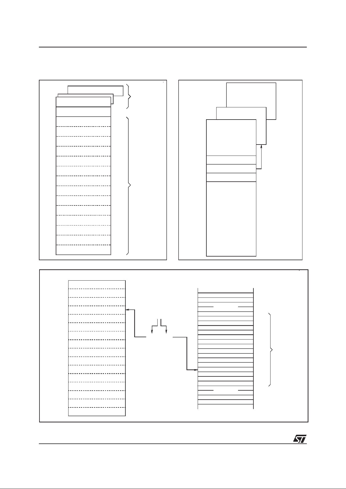
2.2.1 Register File
The Register File consists of (see Figure 12):
– 224 general purpose registers (Group 0 to D,
registers R0 to R223)
– 6 system registers in the System Group (Group
E, registers R224 to R239)
– Up to 64 pages, depending on device configura-
tion, each containing up to 16 registers, mapped
to Group F (R240 to R255), see Figure 13.
Figure 11. Single Program and Data Memory Address Space
3FFFFFh
3F0000h
3EFFFFh
3E0000h
20FFFFh
02FFFFh
020000h
01FFFFh
010000h
00FFFFh
000000h
8
7
6
5
4
3
2
1
0
63
62
2
1
0
Address 16K Pages 64K Segments
up to 4 Mbytes
Data
Code
255
254
253
252
251
250
249
248
247
9
10
11
21FFFFh
210000h
133
134
135
33
Reserved
132
9
26/320
ST92F120 - DEVICE ARCHITECTURE
MEMORY SPACES (Cont’d)
Figure 12. Register Groups Figure 13. Page Pointer for Group F mapping
Figure 14. Addressing the Register File
F
E
D
C
B
A
9
8
7
6
5
4
3
PAGED REGISTERS
SYSTEM REGISTERS
2
1
0
00
15
255
240
239
224
223
VA00432
UP TO
64 PAGES
GENERAL
REGISTERS
PURPOSE
224
PAGE 63
PAGE 5
PAGE 0
PAGE POINTER
R255
R240
R224
R0 VA00433
R234
REGISTERFILE
SYSTEM REGISTERS
GROUP D
GROUP B
GROUP C
(1100)
(0011)
R192
R207
255
240
239
224
223
F
E
D
C
B
A
9
8
7
6
5
4
3
2
1
0
15
VR000118
00
R195
R195
(R0C3h)
PAGED REGISTERS
9

27/320
ST92F120 - DEVICE ARCHITECTURE
MEMORY SPACES (Cont’d)
2.2.2 Register Addressing
Register File registers, including Group F paged
registers (but excluding Group D), may be addressed explicitly by means of a decimal, hexadecimal or binary address; thus R231, RE7h and
R11100111b represent the same register (see
Figure 14). Group D registers can only be addressed in Working Register mode.
Note that an upper case “R” is used to denote this
direct addressing mode.
Working Registers
Certain types of instruction require that registers
be specified in the form “rx”, where x is in the
range 0 to 15:these are known as Working Registers.
Note thata lower case “r” isusedto denote thisindirect addressing mode.
Two addressing schemes are available: a single
group of 16 working registers, or two separately
mapped groups,each consisting of 8 working registers. These groups may be mapped starting at
any 8 or 16 byte boundary in the register file by
means of dedicated pointer registers. This technique is described in more detail in Section 2.3.3
Register Pointing Techniques, and illustrated in
Figure 15 and in Figure16.
System Registers
The 16 registers in Group E (R224 to R239) are
System registers and may be addressed using any
of the register addressing modes. These registers
are described in greater detail in Section 2.3 SYSTEM REGISTERS.
Paged Registers
Up to 64 pages, each containing 16 registers, may
be mapped to Group F. These are addressed using any register addressing mode, in conjunction
with the Page Pointer register, R234, which is one
of the System registers. This register selects the
page to be mapped to Group F and, once set,
does not need to be changed if two or more registers on the same page are to be addressed in succession.
Therefore if the PagePointer, R234, is set to 5,the
instructions:
spp #5
ld R242, r4
will load the contents of working register r4 into the
third register of page 5 (R242).
These paged registers hold data and control information relating to the on-chip peripherals, each
peripheral always being associated with the same
pages and registers to ensure code compatibility
between ST9+ devices. The number of these registers therefore depends on the peripherals which
are present in the specific ST9+ family device. In
other words, pages only exist if the relevant peripheral is present.
Table 5. Register File Organization
Hex.
Address
Decimal
Address
Function
Register
File Group
F0-FF 240-255
Paged
Registers
Group F
E0-EF 224-239
System
Registers
Group E
D0-DF 208-223
General
Purpose
Registers
Group D
C0-CF 192-207 Group C
B0-BF 176-191 Group B
A0-AF 160-175 Group A
90-9F 144-159 Group 9
80-8F 128-143 Group 8
70-7F 112-127 Group 7
60-6F 96-111 Group 6
50-5F 80-95 Group 5
40-4F 64-79 Group 4
30-3F 48-63 Group 3
20-2F 32-47 Group 2
10-1F 16-31 Group 1
00-0F 00-15 Group 0
9

28/320
ST92F120 - DEVICE ARCHITECTURE
2.3 SYSTEM REGISTERS
The System registers are listed in Table 6. They
are used to perform all the important system settings. Their purpose is described in the following
pages. Refer to the chapter dealing with I/O for a
description of the PORT[5:0] Data registers.
Table 6. System Registers (Group E)
2.3.1 Central Interrupt Control Register
Please referto the ”INTERRUPT” chapter for a detailed description of the ST9 interrupt philosophy.
CENTRAL INTERRUPT CONTROL REGISTER
(CICR)
R230 - Read/Write
Register Group: E (System)
Reset Value: 1000 0111 (87h)
Bit 7 = GCEN:
Global Counter Enable
.
This bit is the Global Counter Enable of the Multifunction Timers. The GCEN bit is ANDed with the
CE bit in theTCR Register (only in devices featuring the MFT Multifunction Timer) in order to enable
the Timerswhenboth bits are set. This bit is set after the Reset cycle.
Note: Ifan MFT is not included in the ST9 device,
then this bit has no effect.
Bit 6 = TLIP:
Top Level Interrupt Pending
.
This bit is set by hardware when a Top Level Interrupt Request is recognized. This bit can also be
set by software to simulate a Top Level Interrupt
Request.
0: No Top Level Interrupt pending
1: Top Level Interrupt pending
Bit 5 = TLI:
Top Level Interrupt bit
.
0: Top Level Interrupt is acknowledged depending
on the TLNM bit in the NICR Register.
1: Top Level Interrupt is acknowledged depending
on the IEN and TLNM bits in the NICR Register
(described in the Interrupt chapter).
Bit 4 = IEN:
Interrupt Enable .
This bit is cleared by interrupt acknowledgement,
and set by interrupt return (iret). IEN is modified
implicitly by iret, ei and di instructions or by an
interrupt acknowledge cycle. It can also be explicitly written by the user, but only when no interrupt
is pending. Therefore, the user should execute a
di instruction (or guarantee by other means that
no interrupt request can arrive) before any write
operation to the CICR register.
0: DisableallinterruptsexceptTop Level Interrupt.
1: Enable Interrupts
Bit 3 = IAM:
Interrupt Arbitration Mode
.
This bit is set and clearedby software to select the
arbitration mode.
0: Concurrent Mode
1: Nested Mode.
Bit 2:0 = CPL[2:0]:
Current Priority Level
.
These three bits record the priority level of the routine currently running (i.e. the Current PriorityLevel, CPL). The highest priority level is represented
by 000, and the lowest by 111. The CPL bits can
be set by hardware or software and provide the
reference according to which subsequent interrupts are eitherleft pending or are allowed to interrupt the current interruptservice routine. When the
current interrupt is replacedby one of a higher priority, the current priority value is automatically
stored until required in the NICR register.
R239 (EFh) SSPLR
R238 (EEh) SSPHR
R237 (EDh) USPLR
R236 (ECh) USPHR
R235 (EBh) MODE REGISTER
R234 (EAh) PAGE POINTER REGISTER
R233 (E9h) REGISTER POINTER 1
R232 (E8h) REGISTER POINTER 0
R231 (E7h) FLAG REGISTER
R230 (E6h) CENTRAL INT. CNTL REG
R229 (E5h) PORT5 DATAREG.
R228 (E4h) PORT4 DATAREG.
R227 (E3h) PORT3 DATAREG.
R226 (E2h) PORT2 DATAREG.
R225 (E1h) PORT1 DATAREG.
R224 (E0h) PORT0 DATAREG.
70
GCE
N
TLIP TLI IEN IAM CPL2 CPL1 CPL0
9

29/320
ST92F120 - DEVICE ARCHITECTURE
SYSTEM REGISTERS (Cont’d)
2.3.2 Flag Register
The Flag Register contains 8 flags which indicate
the CPU status. During an interrupt, the flag register is automatically stored in the systemstack area
and recalled at the end of the interrupt service routine, thus returning the CPU to its original status.
This occurs for all interrupts and, when operating
in nested mode, up to seven versions of the flag
register may be stored.
FLAG REGISTER (FLAGR)
R231- Read/Write
Register Group: E (System)
Reset value: 0000 0000 (00h)
Bit 7 = C:
Carry Flag
.
The carry flag is affected by:
Addition (add, addw, adc, adcw),
Subtraction (sub, subw, sbc, sbcw),
Compare (cp, cpw),
Shift Right Arithmetic (sra, sraw),
Shift Left Arithmetic (sla, slaw),
Swap Nibbles (swap),
Rotate (rrc, rrcw, rlc, rlcw, ror,
rol),
Decimal Adjust (da),
Multiply and Divide (mul, div, divws).
When set, it generally indicates a carry out of the
most significant bit position of the register being
used as an accumulator (bit 7 for byte operations
and bit 15 for word operations).
The carry flag can be set by the Set Carry Flag
(scf) instruction, cleared by the Reset Carry Flag
(rcf) instruction, and complemented by the Complement Carry Flag (ccf) instruction.
Bit 6 = Z:
Zero Flag
. The Zero flag is affected by:
Addition (add, addw, adc, adcw),
Subtraction (sub, subw, sbc, sbcw),
Compare (cp, cpw),
Shift Right Arithmetic (sra, sraw),
Shift Left Arithmetic (sla, slaw),
Swap Nibbles (swap),
Rotate (rrc, rrcw, rlc, rlcw, ror,
rol),
Decimal Adjust (da),
Multiply and Divide (mul, div, divws),
Logical (and, andw, or, orw, xor,
xorw, cpl),
Increment and Decrement (inc, incw, dec,
decw),
Test (tm, tmw, tcm, tcmw, btset).
Inmostcases, theZeroflagissetwhenthecontents
of the register being used as an accumulator become zero, following one of the above operations.
Bit 5 = S:
Sign Flag
.
The Sign flag is affected by the same instructions
as the Zero flag.
The Sign flag is set when bit 7 (for a byte operation) or bit 15 (for a word operation) of the register
used as an accumulator is one.
Bit 4 = V:
Overflow Flag
.
The Overflow flag is affected by the same instructions as the Zero and Sign flags.
When set, the Overflow flag indicates that a two’scomplement number, in a result register, is in error, since it has exceeded the largest (or is less
than the smallest), number that can be represented in two’s-complement notation.
Bit 3 = DA:
Decimal Adjust Flag
.
The DA flag is used for BCD arithmetic. Since the
algorithm for correcting BCD operations is different for addition and subtraction, this flag is used to
specify which type of instruction was executed
last, so that the subsequent Decimal Adjust (da)
operation can perform its function correctly. The
DA flag cannot normally be used as a test condition by the programmer.
Bit 2 = H:
Half Carry Flag.
The H flag indicates a carry out of (or a borrow into) bit 3, as the result of adding or subtracting two
8-bit bytes, each representing two BCDdigits. The
H flag is used by the Decimal Adjust (da) instruction to convert the binary result of a previous addition or subtraction into the correct BCD result. Like
the DA flag, this flag is not normally accessed by
the user.
Bit 1 = Reserved bit (must be 0).
Bit 0 = DP:
Data/Program Memory Flag
.
This bit indicates the memory area addressed. Its
value is affected by the Set Data Memory (sdm)
and Set Program Memory (spm) instructions. Refer to the Memory Management Unit for further details.
70
C Z S V DA H - DP
9

30/320
ST92F120 - DEVICE ARCHITECTURE
SYSTEM REGISTERS (Cont’d)
If the bit is set, data is accessed using the Data
Pointers (DPRs registers), otherwise it is pointed
to by the Code Pointer (CSR register); therefore,
the user initialization routine must include a Sdm
instruction. Note that code is always pointed to by
the Code Pointer (CSR).
Note: In the ST9+, the DP flag is only for compatibility with software developed for the first generation of ST9 devices. With the single memory addressing space, its use is now redundant. It must
be kept to 1 with a Sdm instruction at the beginning
of the program toensure a normal use of the different memory pointers.
2.3.3 Register Pointing Techniques
Two registers within the System register group,
are usedas pointers to the working registers. Register Pointer 0 (R232) may be used on its own as a
single pointer to a 16-register working space, or in
conjunction with Register Pointer 1 (R233), to
point to two separate 8-register spaces.
For the purpose of register pointing, the 16 register
groups of the register file are subdivided into 32 8register blocks. The values specified with the Set
Register Pointer instructions refer to the blocks to
be pointedto in twin 8-register mode, or to the lower 8-register block location in single 16-register
mode.
The Set Register Pointer instructions srp, srp0
and srp1 automatically inform the CPU whether
the Register File is to operate in single 16-register
mode or in twin 8-register mode. The srp instruction selects the single 16-register group mode and
specifies the location of the lower 8-register block,
while the srp0 and srp1 instructions automatically select the twin 8-register group mode and specify the locations of each 8-register block.
There is no limitation on the order or position of
these register groups, other than that they must
start on an 8-register boundary in twin 8-register
mode, or on a 16-register boundary in single 16register mode.
The block number should always be an even
number in single 16-register mode. The 16-register group will always start at the block whose
number is the nearest even number equal to or
lower than the block number specified in the srp
instruction. Avoid using odd block numbers, since
this can be confusing if twin mode is subsequently
selected.
Thus:
srp #3 will be interpreted as srp #2 and will al-
low using R16 ..R31 as r0 .. r15.
In single 16-register mode, the working registers
are referred to as r0 to r15. In twin 8-register
mode, registers r0 to r7 are in the block pointed
to by RP0 (by means of the srp0 instruction),
while registers r8 to r15 are in the block pointed
to by RP1 (by means of the srp1 instruction).
Caution:
Group D registers can only be accessed
as working registers using the Register Pointers,
or by means of the Stack Pointers. They cannot be
addressed explicitly in the form “Rxxx”.
9
 Loading...