

SGS Thomson Microelectronics ST9293J5, ST9293J7, ST9293J3, ST9293J1, ST9293 Datasheet
ON SCREEN DISPLAY AND A/D CONVERTER
Register oriented 8/ 16 bit C OR E with
RUN, WFI and HALT modes
Minimum instruc tion cycle time: 500ns
(12MHz internal)
16 to 48K bytes of ROM,
256 to 768 bytes of RAM,
224 general purpose registers available as RAM,
accumulators or index registers (Register File)
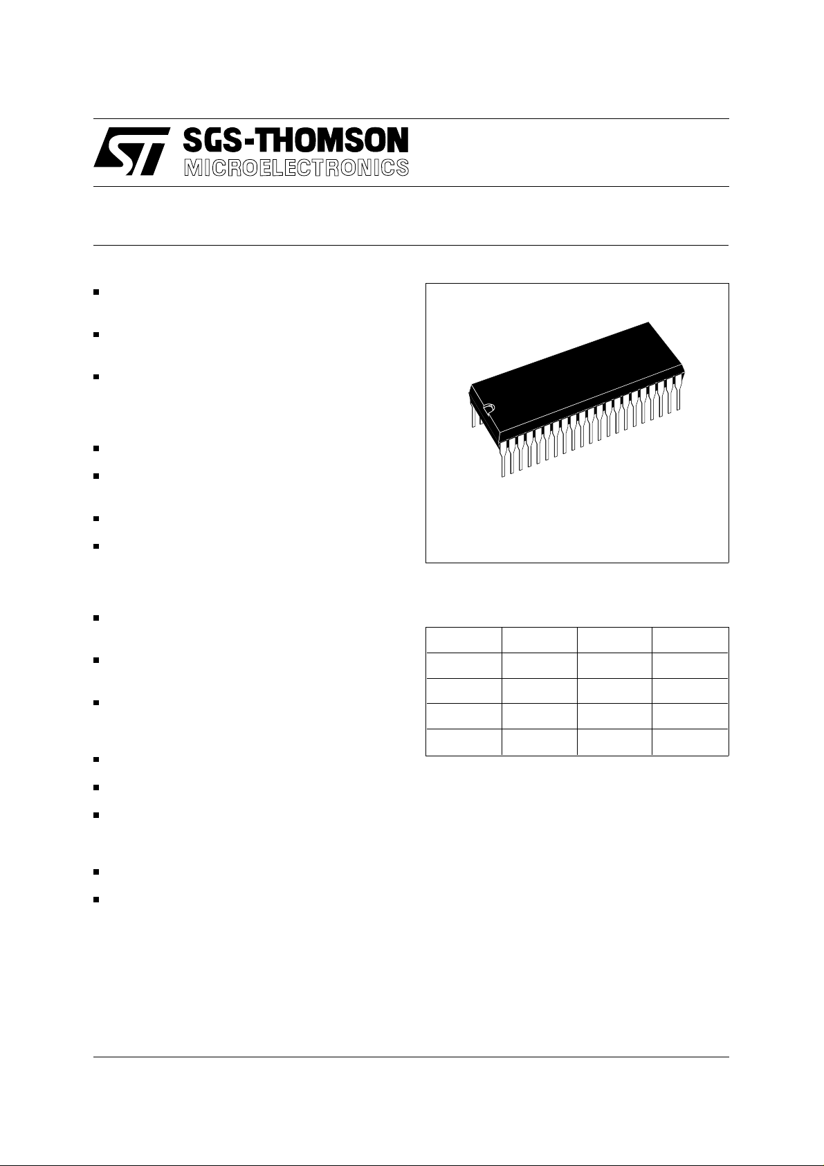
42-lead Shrink DIP package
Interrupt handler and Serial P eripheral Interface
as standard features
31 fully programmable I/O pins
ST9293
48K ROM HCMOS MCUs WITH
FUNCTIONAL DESCRIPTION
PSDIP42
34 character x15 rows software programmable
On Screen Dis play module with colour, italic, underline, flash, transparent and fringe attribute
options
16 bit Timer with 8 bit Presc aler, able to be used
as a Watchdog Timer
16-bit programmable Slice Timer with 8-bit prescaler
4 channel Analog to Digital Converter, with integral sample and hold, fast 5.75µs conversion
time, 6-bit guaranteed resolution
Rich Instruct ion S et and 14 A ddressing modes
Division-by-Zero trap generati on
Versatile Development tools, including assembler,
linker, C-c ompiler, a rchiver, grap hic oriented debugger and hardware emulators
Real Time Operating System
Windowed EPROM parts available for prototyp-
ing and pre-production development phases
(Ordering Information at the end of the Datashe et)
DEVICE SUMMARY
Device ROM RAM PACKAGE
ST9293J7 48K 768 PSDIP42
ST9293J5 32K 640 PSDIP42
ST9293J3 24K 512 PSDIP42
ST9293J1 16K 256 PSDIP42
May 1993
This is Preliminary Data from SGS-THOMSON. Details are subject to change without notice.
1/4

ST9293
1.1GENERAL DESCRIPTION
The ST9293 is a ROM member of the ST9 family of
microcontrollers, completely developed and produced by SGS-THOMSON Microelectronics using
a proprietary n-well HCMOS process.
The ROM parts are fully compatible with their
EPROM versions, which may be used for the prototyping and pre-production phases of development, and can be configured as standalone
microcontrollers wit h 48K /32K /24K/ 16 by tes of on chip ROM.
The nucleus of the ST9293 is the advanced Core
which includes the Central Processing Unit (C PU),
the Register File, a 16-bit Timer/Watchdog with 8bit Prescaler, a Serial P eripheral Interface support ing S-bus, I
8-bit I/O ports. The Core has independent memory
and register buses allowing a high degree of pipelining to add to the efficiency of the code execution
speed of the extensive instruction set.Th e powerful
I/O capabilities demanded by microcontroller applications are fulfilled by the ST9293 wit h up to 31/41
I/O lines dedicated to digital Input/Output.
These lines are grouped into up to six I/O Ports and
can be configured on a bit basis under software
2
C-bus and IM-bus Interface, plus two
control to provide timing, status signals, timer inputs and outputs, analog inputs, ext ernal interrupts
and serial or parallel I/O.
Three basic memory spaces are available to support this wide range of configurations: Program
Memory, Data Memory and the Register File,
which includes the control and status registers of
the on-chip peripherals.
The 16-bit Slice Tim er with an 8-bit Prescaler and 6
operating modes allows simple use for waveformgeneration and measurement, PWM functions
and many other system timing functions.
The human interface is provided by the On S creen
Display module, this can produce up to 8 lines of of
up to 34 characters from a ROM defined 128 character set. The 9x13 character can be modified by 4
different pixel sizes, with character rounding, and
formed into words with colour and format attributes.
In addition there is a 4 channel Analog to Digital
Converter with integral s ample and hold, fast 5.5µs
conversion time and 6-bit guaranteed resolution.
Figure 1-1. ST9293 Block Diag ram
16 to 48k x 8
ROM
I/O PORT 0
8
ROM RAM
J7
J5
J3
J1
48K 76 8
32K 64 0
24K 51 2
16K 256
256 to 768
RAM
MEMORY BUS ( Address & Data )
I/O PORT 2
( SPI )
8
256 Bytes
REGISTER F ILE
REGISTER BUS ( Address & Data )
VSYNC
ON SCREEN
DISPLAY
PLL
HSYNC
PLLR
PLLF
I/O PORT 3
AV
DD
16-Bit TIMER / WATCHDOG + SPI
CPU
A/D
CONVERTER
5
( Analog Inputs )
I/O PORT 4
3
SLICE
TIMER
I/O PORT 5
( Control Bus )
( Colour )
7
VR0B1749
2/4
 Loading...