

SGS Thomson Microelectronics ST9291J6, ST9291J7, ST9291J5, ST9291J4, ST9291J3 Datasheet
...
ST9291
July 1995
16-48K ROM HCMOS MCU WITH
ON SCREEN DISP L A Y AND VOL TA GE TUNINGOU TP UT
(Ordering Information at the end of the Datasheet)
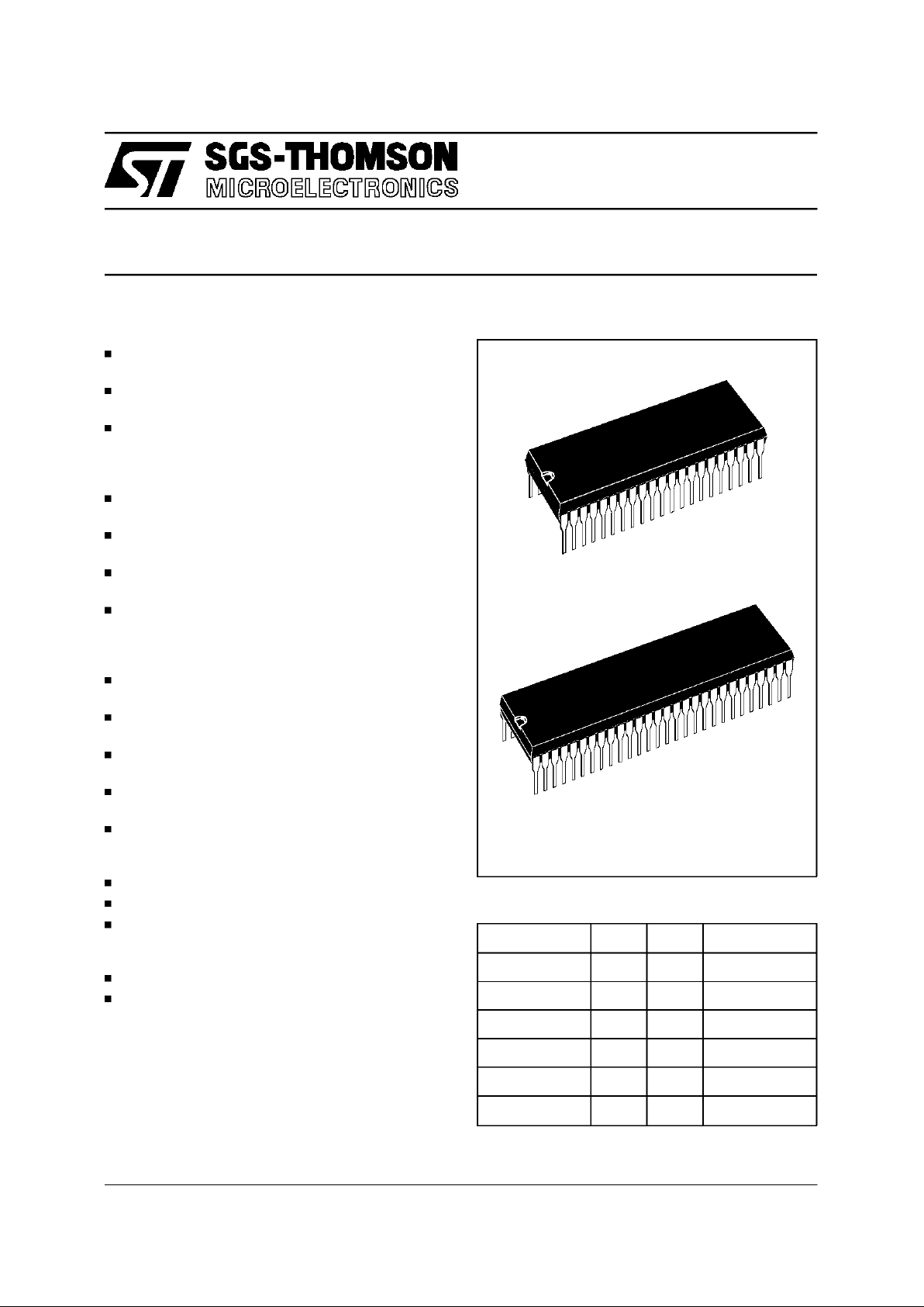
PSDIP42
PSDIP56
Device ROM RAM PACKAGE
ST9291J2/N2 16K 384 PSDIP42/56
ST9291J3/N3 16K 640 PSDIP42/56
ST9291J4/N4 24K 384 PSDIP42/56
ST9291J5/N5 24K 640 PSDIP42/56
ST9291J6/N6 32K 640 PSDIP42/56
ST9291J7/N7 48K 640 PSDIP42/56
DEVICE SUMMARY
Registeroriented8/16 bit COREwith
RUN,WFI andHALT modes
Minimuminstructioncycle time: 500ns
(12MHzinternal)
16 to 48K bytes of ROM,
384/640bytes of RAM,
224generalpurposeregistersavailableasRAM,
accumulatorsor index registers(RegisterFile)
42-leadShrink DIP packageor
56-lead ShrinkDIP package
Interrupthandler and Serial Peripheral Interface
as standardfeatures
31 (42 pin package) / 42 (56 pin package) fully
programmableI/Opins
34 character x15 rows software programmable
On ScreenDisplaymodulewith colour, italic,underline, flash, transparent and fringe attribute
options
14-bit Voltage Synthesis for tuning reference
voltage.
8 8-bit PWM D/A outputswithrepetitionfrequency
2 to 32kHz and12VOpenDrain Capability
16 bit Timer with 8 bitPrescaler, able to beused
as a WatchdogTimer
16-bitprogrammableSlice Timer with 8-bit prescaler
3 channelAnalog to DigitalConverter, withintegral sample and hold, fast 5.75µs conversion
time,6-bit guaranteedresolution
RichInstruction Set and 14 Addressingmodes
Division-by-Zero trap generation
VersatileDevelopmenttools,includingassembler,
linker, C-compiler, archiver,graphic oriented debuggerandhardware emulators
Real TimeOperating System
Windowed EPROM parts available for prototyp-
ing andpre-productiondevelopmentphases
FUNCTIONAL DESCRIPTION
1/20
3
19
20
24
23
2221
VR01740B
40
2
1
42
41
Figure 1. 42 Pin Shrink DIP Pinout
Pin
Pin
name
1 P2.0/INT7
2 RESET
3 P0.7
4 P0.6
5 P0.5
6 P0.4
7 P0.3
8 P0.2
9 P0.1
10 P0.0
11 P3.7
12 P3.6
13 P3.5
14 P3.4
15 P3.3/B
16 P3.2/G
17 P3.1/R
18 P3.0/FB
19 P5.1/SDIO
20 P5.0/SCK/INT2
21 V
DD
Pin
Pin
name
42 P2.1/INT5/AIN1
41 P2.2/INT0/AIN2
40 P2.3/INT6/VSO1
39 P2.4/NMI
38 P2.5/AIN3/VSO2
37 OSCIN
36 OSCOUT
35 P4.7/PWM7/
EXTRG (AD)
34 P4.6/PWM6
33 P4.5/PWM5
32 P4.4/PWM4
31 P4.3/PWM3
30 P4.2/PWM2
29 P4.1/PWM1
28 P4.0/PWM0
27 VSYNC
26 HSYNC
25 AV
DD
24 PLLR
23 PLLF
22 V
SS
ST9291JPin Description
Pin
Pin
name
1 P2.1/INT5/AIN1
2 P2.0/INT7
3 RESET
4P0.7
5P0.6
6P0.5
7N.C
.(1)
8P0.4
9P0.3
10 P0.2
11 P0.1
12 P0.0
13 N.C.
(1)
14 V
DD
(2)
15
N.C.
(1)
16 P3.7
17 P3.6
18 P3.5
19 P3.4
20 P3.3/B
21 P3.2/G
22 P3.1/R
23 P3.0/FB
24 P5.3
25 P5.2
26 P5.1/SDIO
27 P5.0/SCK/INT2
28 V
DD
(2)
Pin
Pin
name
56 P2.2/INT0/AIN2
55 P2.3/INT6/VSO1
54 P2.4/NMI
53 P2.5/AIN3/VSO2
52 P1.0
51 P1.1
50 P1.2
49 P1.3
48 P1.4
47 P1.5
46 P1.6
45 P1.7
44 OSCIN
43 OSCOUT
42
P4.7/PWM7/
EXTRG (AD)
41 P4.6/PWM6
40 P4.5/PWM5
39 P4.4/PWM4
38 P4.3/PWM3
37 P4.2/PWM2
36 P4.1/PWM1
35 P4.0/PWM0
34 VSYNC
33 HSYNC
32 AV
DD
31 PLLR
30 PLLF
29 V
SS
ST9291NPin Description
3
26
27
31
30
2928
VR01740A
54
2
1
56
55
Figure2. 56 PinShrink DIP Pinout
Notes (N Package only) :
1. N.C. means “not connected”
2. Pins 14 and 28 (VDD) areinternally connected
ST9291
2/20

GENERALDESCRIPTION
The ST9291isa ROMmemberof the ST9familyof
microcontrollers, completely developed and produced by SGS-THOMSON Microelectronicsusing
a proprietaryn-well HCMOS process.
The ROM parts are fully compatible with their
EPROMand OTP (One-TimeProgrammable)versions, which may be used for the prototypingand
pre-productionphasesof development.
The nucleus of the ST9291 is the advancedST9
Core which includes the Central Processing Unit
(CPU), the Register File, a 16-bit Timer/Watchdog
with 8-bit Prescaler, a Serial Peripheral Interface
supporting S-bus, I
2
C-bus and IM-bus Interface,
plus two 8-bitI/O ports. TheCore hasindependent
memory andregisterbuses allowinga high degree
of pipelining to add to the efficiency of the code
executionspeed of the extensive instructionset.
The powerful I/O capabilitiesdemandedby microcontroller applications are fulfilled by the ST9291
with up to 32/42 I/O lines dedicated to digital Input/Output. These lines are groupedinto up to six
I/O Ports and can be configuredon a bit basis under software control to provide timing, status sig-
nals, timer inputs and outputs, analog inputs, external interrupts, OSD (On Screen Display) output
and serialor parallelI/O.
Three basic memoryspaces are available to support this wide range of configurations: Program
Memory, Data Memory and the Register File,
which includes the control and status registers of
the on-chipperipherals.
The humaninterface isprovided by the On Screen
Displaymodule, this can produce up to 15 lines of
up to 34 charactersfrom a ROM defined 128 character set.The 9x13 character canbe modified by4
different pixel sizes, with character rounding, and
formed into words with colour and format attributes.
A 14-bit VS (Voltage Synthesis) output using the
PWM (Pulse Width Modulation)/BRM (Bit Rate
Modulation)is present to generatetuning voltages
for low-mid range TV set applications. The tuning
voltage is output on one of two separate output
pins.
A 16-bit Slice Timer with an 8-bit Prescaleris also
present.
CPU
16-Bit TIMER/WATCHDOG+SPI
SLICE
TIMER
VOLTAGE
SYNTHESIS
I/O PORT 0
8
I/O PORT
3
7
On Screen
Display
PLL
HSYNC
PLLR
PLLF
AV
DD
VSYNC
I/O PORT 4
P.W.M.
Outputs
8
P.W.M.
D/A
Converter
I/O PORT 2
( Analog Inputs )
6
A/D
Converter
I/O PORT 5
( SPI )
2
MEMORY BUS( Address& Data )
REGISTERBUS( Address& Data )
Note : 42 SDIP shown
VR01995E
16 k / 48 k Bytes
ROM or EPROM
(1)
384 / 640 Bytes
RAM
256 Bytes
REGISTER FILE
Figure 3. ST9291 Block Diagram
Note 1. EPROM version only
ST9291
3/20

The control of TV or Satellitereceiver setting can
be done by up to eight 8-bit PWM outputs, with a
frequency maximum of 23,437Hz at 8-bit resolution (INTCLK = 12MHz). Low resolutions with
higher frequencyoperationcan be programmed.
Inadditionthereis a3 channelAnalogtoDigitalConverterwithintegralsampleandhold,fast5.75µscon-
versiontimeand6-bitguaranteedresolution.
PIN DESCRIPTION
VSYNC.
VerticalSync.
Verticalvideosynchronisa-
tion inputto OSD. Positiveor negativepolarity.
HSYNC.
Horizontal Sync.
Horizontal video synchronisationinput to OSD. Positiveor negativepolarity.
PLLF.
PLL Filterinput.
Filterinput for the OSD for
PLL feed-back.
PLLR.
PLL Resistor connection pin.
For resistor
connectionto select the PLL gain adjust.
RESET.
Reset(input,active low).
TheST9is initialisedbytheResetsignal.WiththedeactivationofRESET, program execution begins from the Program
memory location pointedto bythe vectorcontained
in programmemorylocations00h and01h.
OSCIN, OSCOUT.
Oscillator (input and output).
These pins connect a parallel-resonant crystal
GENERALDESCRIPTION (Continued)
(24MHz maximum), or an external source to the
on-chipclockoscillatorandbuffer.OSCINis theinput ofthe oscillatorinverter andinternalclock generator; OSCOUT is the output of the oscillator
inverter.
AV
DD
. AnalogVDDof PLL. This pin must betied to
V
DD
externallyto theST9291.
V
DD
. MainPowerSupply Voltage(5V±10%)
V
SS
. Digital Circuit Ground.
P0.0-P0.7, P2.0-P2.5, P3.0-P3.7, P4.0-P4.7,
P5.0-P5.1(J suffix)
P0.0-P0.7, P1.0-P1.7, P2.0-P2.5, P3.0-P3.7,
P4.0-P4.7,P5.0-P5.3 (N suffix)
I/O Port Lines (In-
put/Output,TTLor CMOScompatible).
32/42lines
grouped into I/O ports, bit programmable under
programcontrolas generalpurposeI/O oras Alternate functions(see next section).
P4.0 - P4.7are high voltage(12V) open drainoutputs. Thevoltage inopen drainoutput modefor all
other I/Obits must not exceed V
DD
.
I/O PortAlternate Functions.
Each pin of the I/O ports of the ST9291 may assume software programmable Alternative Functionsas shownin the Pin ConfigurationDrawings.
Table1 shows the Functionsallocated to each I/O
Port pin.
ST9291
4/20
PIN DESCRIPTION(Continued)
I/O PORT
Name Function Alternate Function
Pin Assignment
Port.bit 9291J 9291N
P0.0 I/O 10 12
P0.1 I/O 9 11
P0.2 I/O 8 10
P0.3 I/O 7 9
P0.4 I/O 6 8
P0.5 I/O 5 6
P0.6 I/O 4 5
P0.7 I/O 3 4
P1.0 I/O - 52
P1.1 I/O - 51
P1.2 I/O - 50
P1.3 I/O - 49
P1.4 I/O - 48
P1.5 I/O - 47
P1.6 I/O - 46
P1.7 I/O - 45
P2.0 INT7 I External Interrupt 7 with Schmitt Trigger 1 2
P2.1 INT5 I External Interrupt 5 with Schmitt Trigger 42 1
P2.1 AIN1 I A/D Analog Input 1 42 1
P2.2 INT0 I External Interrupt 0 41 56
P2.2 AIN2 I A/D Analog Input 2 41 56
P2.3 INT6 I External Interrupt 6 40 55
P2.3 VSO1 O Voltage Synthesis Output 1 40 55
P2.4 NMI I Non-Maskable Interrupt 39 54
P2.5 AIN3 I A/D Analog Input 3 38 53
P2.5 VSO2 O Voltage Synthesis Output 2 38 53
P3.0 FB O Fast Blanking OSD output 18 23
P3.1 R O Red Video Colour OSD output 17 22
P3.2 G O Green Video Colour OSD output 16 21
P3.3 B O Blue Video Colour OSD output 15 20
Table 1.ST9291 I/O Port Alternative Function Summary
ST9291
5/20
PIN DESCRIPTION(Continued)
I/O PORT
Name Function Alternate Function
Pin Assignment
Port.bit 9291J 9291N
P3.4 I/O 14 19
P3.5 I/O 13 18
P3.6 I/O 12 17
P3.7 I/O - 16
P4.0 PWM0 O PWM Output 0 28 35
P4.1 PWM1 O PWM Output 1 29 36
P4.2 PWM2 O PWM Output 2 30 37
P4.3 PWM3 O PWM Output 3 31 38
P4.4 PWM4 O PWM Output 4 32 39
P4.5 PWM5 O PWM Output 5 33 40
P4.6 PWM6 O PWM Output 6 34 41
P4.7 PWM7 O PWM Output 7 35 42
P4.7 EXTRG I A/D External Trigger 35 42
P5.0 SCK O SPI Serial Clock
(1)
20 27
P5.0 INT2 I External Interrupt 2
(1)
20 27
P5.1 SDIO I/O SPI Serial Data Input/Output
(1)
19 26
P5.2 I/O - 25
P5.3 I/O - 24
Notes.
1. The alternate functions of SCK/INT2 and SDIO may be swapped by using the SWAP Register Function.
2. Schmitt trigger options are available as a mask option for any input pin.
Table 1. ST9291 I/O PortAlternativeFunction Summary(Continued)
ST9291
6/20
 Loading...