

SGS Thomson Microelectronics ST7FSCR1R4, ST7FSCR1E4, ST7SCRDIE, ST7SCR1E4, ST7SCR1R4 Datasheet
...
Rev. 1.3
March 2003 1/102
ST7SCR
8-BIT LOW-POWER, FULL-SPEED USB MCU WITH 16K
FLASH , 768 RAM, SMARTCARD I/F, TIMER
■ Memories
– Up to 16K of ROM or High Density Flash (HD-
Flash) program memory wi th read/write protection, HDFlash In-Circuit and In-Application
Programming. 100 write/erase cycles guaranteed, data retention: 20 years at 55°C
– Up to 768 bytes of RAM in cluding up to 128
bytes stack and 256 bytes USB buffer
■ Clock , Res et and Supp ly M a nagemen t
– Low Voltage Reset
– 2 power saving modes: Halt and Wait modes
– PLL for generating 48 MHz USB clock using a
4 MHz crystal
■ Interrupt Management
– Nested Interrupt Controller
■ USB (Universal Serial Bus) Interface
– 256-byte buffer for full speed bulk, control and
interrupt transfer types compliant with USB
specification (version 2.0)
– On-Chip 3.3V USB voltage regulator and
transceivers with software power-down
– 7 USB Endpoints:
One 8-byte Bidirectional Control Endpoint
One 64-byte In Endpoint,
One 64-byte Out Endpoint
Four 8-byte In Endpoints
■ 35 or 4 I/O ports:
– Up to 4 LED outputs with software program -
mable constant current (3 or 7 mA).
– 2 General purpose I/Os program mable as in-
terru p ts
– Up to 8 line inputs programmable as interrupts
– Up to 20 Outputs
– 1 line assigned by default as st atic input after
reset
■ ISO7816-3 UART Interface:
– 4 Mhz Clock generation
– Synchronous/Asynchronous protocols (T=0,
T=1)
– Automatic retry on parity error
– Programmable Baud rate from 372 clock puls-
es up to 11.625 clock pulses (D=32/F=372)
– Card Insertion/Removal Detection
■ Smartcard Power Suppl y:
– Selectable card V
CC
1.8V, 3V, and 5V
– Internal Step-up converter for 5V supplied
Smartcards (with a current of up to 55mA) us-
ing only two external components.
– Programmable Smartcard Internal Voltage
Regulator (1.8V to 3.0V) with current overload
protection and 4 KV ESD protection (Human
Body Model) for all Smartcard Interface I/Os
■ One 8-bit Timer
– Time Base Unit (TBU) for generating periodic
interrupts.
■ Development Tools
– Full hardware/software development package
Table 1. Device Summa ry
TQFP64 14x14
SO24
Features ST7FSCR1R4 ST7SCR1R4 ST7FSCR1E4 ST7SCR1E4
Program memory 16K FLASH 16K ROM 16K FLASH 16K ROM
User RAM (stack) - bytes 768 (128)
Peripherals USB Full-Speed (7 Ep), TBU, Watchdog timer, ISO7816-3 Interface
Operating Supply 4.0 to 5.5V
Package TQFP64 SO24
CPU Frequency 4 or 8 Mhz
Operating temperature 0°C to +70°C
1

Table of Cont ents
102
2/102
ST7SCR . . . . . . . . . . . . . . . . . . . . . . . . . . . . . . . . . . . . . . . . . . . . . . . . . . . . . . 1
1 INTRODUCTION . . . . . . . . . . . . . . . . . . . . . . . . . . . . . . . . . . . . . . . . . . . . . . . . . . . . . . . . . . . . . . 4
2 PIN DESCRIPTION . . . . . . . . . . . . . . . . . . . . . . . . . . . . . . . . . . . . . . . . . . . . . . . . . . . . . . . . . . . . 5
3 REGISTER & MEM ORY MAP . . . . . . . . . . . . . . . . . . . . . . . . . . . . . . . . . . . . . . . . . . . . . . . . . . . 11
4 FLASH PROGRAM MEMORY . . . . . . . . . . . . . . . . . . . . . . . . . . . . . . . . . . . . . . . . . . . . . . . . . . 14
4.1 INTRODUCTION . . . . . . . . . . . . . . . . . . . . . . . . . . . . . . . . . . . . . . . . . . . . . . . . . . . . . . . 14
4.2 MAIN FEATURES . . . . . . . . . . . . . . . . . . . . . . . . . . . . . . . . . . . . . . . . . . . . . . . . . . . . . . 14
4.3 STRUCTURE . . . . . . . . . . . . . . . . . . . . . . . . . . . . . . . . . . . . . . . . . . . . . . . . . . . . . . . . . . 14
4.4 ICP (IN-CIRCUIT PR OGRAMMING) . . . . . . . . . . . . . . . . . . . . . . . . . . . . . . . . . . . . . . . . 15
4.5 IAP (IN-APPLICATION PROGRAMMING) . . . . . . . . . . . . . . . . . . . . . . . . . . . . . . . . . . . 15
4.6 PROGRAM MEMORY READ-O UT PROTECTION . . . . . . . . . . . . . . . . . . . . . . . . . . . . . 16
5 CENTRAL PROCESSING UNIT . . . . . . . . . . . . . . . . . . . . . . . . . . . . . . . . . . . . . . . . . . . . . . . . . 17
5.1 INTRODUCTION . . . . . . . . . . . . . . . . . . . . . . . . . . . . . . . . . . . . . . . . . . . . . . . . . . . . . . . 17
5.2 MAIN FEATURES . . . . . . . . . . . . . . . . . . . . . . . . . . . . . . . . . . . . . . . . . . . . . . . . . . . . . . 17
5.3 CPU REGISTERS . . . . . . . . . . . . . . . . . . . . . . . . . . . . . . . . . . . . . . . . . . . . . . . . . . . . . . 17
6 SUPPLY, RESET AND CLOCK MANAGEMENT . . . . . . . . . . . . . . . . . . . . . . . . . . . . . . . . . . . . 20
6.1 CLOCK SYSTEM . . . . . . . . . . . . . . . . . . . . . . . . . . . . . . . . . . . . . . . . . . . . . . . . . . . . . . . 20
6.2 RESET SEQUENCE MANAGER (RSM) . . . . . . . . . . . . . . . . . . . . . . . . . . . . . . . . . . . . . 22
7 INTERRUPTS . . . . . . . . . . . . . . . . . . . . . . . . . . . . . . . . . . . . . . . . . . . . . . . . . . . . . . . . . . . . . . . 23
7.1 INTRODUCTION . . . . . . . . . . . . . . . . . . . . . . . . . . . . . . . . . . . . . . . . . . . . . . . . . . . . . . . 23
7.2 MASKING AND PROCESSING FLOW . . . . . . . . . . . . . . . . . . . . . . . . . . . . . . . . . . . . . . 23
7.3 INTERRUPTS AND LOW POWER MODES . . . . . . . . . . . . . . . . . . . . . . . . . . . . . . . . . . 25
7.4 CONCURRENT & NESTED MANAGEMENT . . . . . . . . . . . . . . . . . . . . . . . . . . . . . . . . . 25
7.5 INTERRUPT REGISTER DESCRIPTION . . . . . . . . . . . . . . . . . . . . . . . . . . . . . . . . . . . . 26
8 POWER SAVING MODES . . . . . . . . . . . . . . . . . . . . . . . . . . . . . . . . . . . . . . . . . . . . . . . . . . . . . 28
8.1 INTRODUCTION . . . . . . . . . . . . . . . . . . . . . . . . . . . . . . . . . . . . . . . . . . . . . . . . . . . . . . . 28
8.2 WAIT MODE . . . . . . . . . . . . . . . . . . . . . . . . . . . . . . . . . . . . . . . . . . . . . . . . . . . . . . . . . . 28
8.3 HALT MODE . . . . . . . . . . . . . . . . . . . . . . . . . . . . . . . . . . . . . . . . . . . . . . . . . . . . . . . . . . 29
9 I/O PORTS . . . . . . . . . . . . . . . . . . . . . . . . . . . . . . . . . . . . . . . . . . . . . . . . . . . . . . . . . . . . . . . . . . 30
9.1 INTRODUCTION . . . . . . . . . . . . . . . . . . . . . . . . . . . . . . . . . . . . . . . . . . . . . . . . . . . . . . . 30
9.2 FUNCTIONAL DESCRIPTION . . . . . . . . . . . . . . . . . . . . . . . . . . . . . . . . . . . . . . . . . . . . 30
9.3 I/O PORT IMPLEMENTATION . . . . . . . . . . . . . . . . . . . . . . . . . . . . . . . . . . . . . . . . . . . . 31
9.4 REGISTER DESCRIPTION . . . . . . . . . . . . . . . . . . . . . . . . . . . . . . . . . . . . . . . . . . . . . . . 34
10 MISCEL LANEOUS REGISTERS . . . . . . . . . . . . . . . . . . . . . . . . . . . . . . . . . . . . . . . . . . . . . . . 36
11 LEDs . . . . . . . . . . . . . . . . . . . . . . . . . . . . . . . . . . . . . . . . . . . . . . . . . . . . . . . . . . . . . . . . . . . . . 39
12 ON-CHIP PERIPHERALS . . . . . . . . . . . . . . . . . . . . . . . . . . . . . . . . . . . . . . . . . . . . . . . . . . . . . 40
12.1 WATCHDOG TIMER (WDG) . . . . . . . . . . . . . . . . . . . . . . . . . . . . . . . . . . . . . . . . . . . . . . 40
12.2 TIME BASE UNIT (TBU) . . . . . . . . . . . . . . . . . . . . . . . . . . . . . . . . . . . . . . . . . . . . . . . . . 42
12.3 USB INTERFACE (USB) . . . . . . . . . . . . . . . . . . . . . . . . . . . . . . . . . . . . . . . . . . . . . . . . . 44
12.4 SMARTCARD INTERFACE (CRD) . . . . . . . . . . . . . . . . . . . . . . . . . . . . . . . . . . . . . . . . . 55
1

Table of Cont ents
3/102
13 INSTRU CTION SET . . . . . . . . . . . . . . . . . . . . . . . . . . . . . . . . . . . . . . . . . . . . . . . . . . . . . . . . . 70
13.1 ST7 ADDRESSING MODES . . . . . . . . . . . . . . . . . . . . . . . . . . . . . . . . . . . . . . . . . . . . . . 70
13.2 INSTRUCTION GROUPS . . . . . . . . . . . . . . . . . . . . . . . . . . . . . . . . . . . . . . . . . . . . . . . . 73
14 ELECTRICAL CHARACTERISTICS . . . . . . . . . . . . . . . . . . . . . . . . . . . . . . . . . . . . . . . . . . . . . 76
14.1 ABSOLUTE MAXIMUM RATINGS . . . . . . . . . . . . . . . . . . . . . . . . . . . . . . . . . . . . . . . . . 76
14.2 RECOMMENDED OPERATING CONDITIONS . . . . . . . . . . . . . . . . . . . . . . . . . . . . . . . 77
14.3 SUPPLY AND RESET CHARACTERISTICS . . . . . . . . . . . . . . . . . . . . . . . . . . . . . . . . . 79
14.4 CLOCK AND TIMING CHARACTERISTICS . . . . . . . . . . . . . . . . . . . . . . . . . . . . . . . . . . 79
14.5 MEMORY CHARACTERISTICS . . . . . . . . . . . . . . . . . . . . . . . . . . . . . . . . . . . . . . . . . . . 82
14.6 SMARTCARD SUPPLY SUPERVISOR ELECTRICAL CHARACTERISTICS . . . . . . . . 82
14.7 EMC CHARACTERIST ICS . . . . . . . . . . . . . . . . . . . . . . . . . . . . . . . . . . . . . . . . . . . . . . . 84
14.8 COMMUNICATION INTERFACE CHARACTERISTICS . . . . . . . . . . . . . . . . . . . . . . . . . 89
15 PACKAGE CHARACTERISTICS . . . . . . . . . . . . . . . . . . . . . . . . . . . . . . . . . . . . . . . . . . . . . . . 90
15.1 PACKAGE MECHANICAL DATA . . . . . . . . . . . . . . . . . . . . . . . . . . . . . . . . . . . . . . . . . . 90
16 DEVICE CONFIGURATION AND ORDERING INFORMATION . . . . . . . . . . . . . . . . . . . . . . . . 92
16.1 DEVICE ORDERING INFORMATION AND TRANSFER OF CUSTOMER CODE . . . . . 93
16.2 DEVELOPMENT T OOLS . . . . . . . . . . . . . . . . . . . . . . . . . . . . . . . . . . . . . . . . . . . . . . . . 95
16.3 ST7 APPLICATION NOTES . . . . . . . . . . . . . . . . . . . . . . . . . . . . . . . . . . . . . . . . . . . . . . 96
17 SUMMARY OF CHANGES . . . . . . . . . . . . . . . . . . . . . . . . . . . . . . . . . . . . . . . . . . . . . . . . . . . . 98
ERRAT A SHEET . . . . . . . . . . . . . . . . . . . . . . . . . . . . . . . . . . . . . . . . . . . . . . 99
18 SILICON IDENTIFICATION . . . . . . . . . . . . . . . . . . . . . . . . . . . . . . . . . . . . . . . . . . . . . . . . . . . . 99
19 REFERENCE SPECIFICATION . . . . . . . . . . . . . . . . . . . . . . . . . . . . . . . . . . . . . . . . . . . . . . . . 99
20 SILICON LIMITATIONS . . . . . . . . . . . . . . . . . . . . . . . . . . . . . . . . . . . . . . . . . . . . . . . . . . . . . . 99
20.1 UNEXPECTED RESET FETCH . . . . . . . . . . . . . . . . . . . . . . . . . . . . . . . . . . . . . . . . . . . 99
20.2 USB: TWO CO NSECUTIVE SETUP TOKENS . . . . . . . . . . . . . . . . . . . . . . . . . . . . . . . . 99
20.3 USB BUFFER SHARED MEMORY ACCESS . . . . . . . . . . . . . . . . . . . . . . . . . . . . . . . . 100
20.4 WDG (WATCHDOG) LIMITATIONS . . . . . . . . . . . . . . . . . . . . . . . . . . . . . . . . . . . . . . . 100
20.5 SUPPLY CURRENT IN HALT MODE (SUSPEND) LIMITATIONS . . . . . . . . . . . . . . . . 100
20.6 START-UP . . . . . . . . . . . . . . . . . . . . . . . . . . . . . . . . . . . . . . . . . . . . . . . . . . . . . . . . . . . 100
20.7 I/O PORT INPUT HIGH LEVEL (VIH) . . . . . . . . . . . . . . . . . . . . . . . . . . . . . . . . . . . . . . 101
21 Devic e Marking . . . . . . . . . . . . . . . . . . . . . . . . . . . . . . . . . . . . . . . . . . . . . . . . . . . . . . . . . . . . 101
22 ERRATA SHEET ReVISION History . . . . . . . . . . . . . . . . . . . . . . . . . . . . . . . . . . . . . . . . . . . 101
1
To obtain the most recent version of this datasheet,
please check at www.st.com>products>technical liter ature>datasheet
Please note that an errata sheet can be found at the end of this document on
page 99.
ST7SCR
4/102
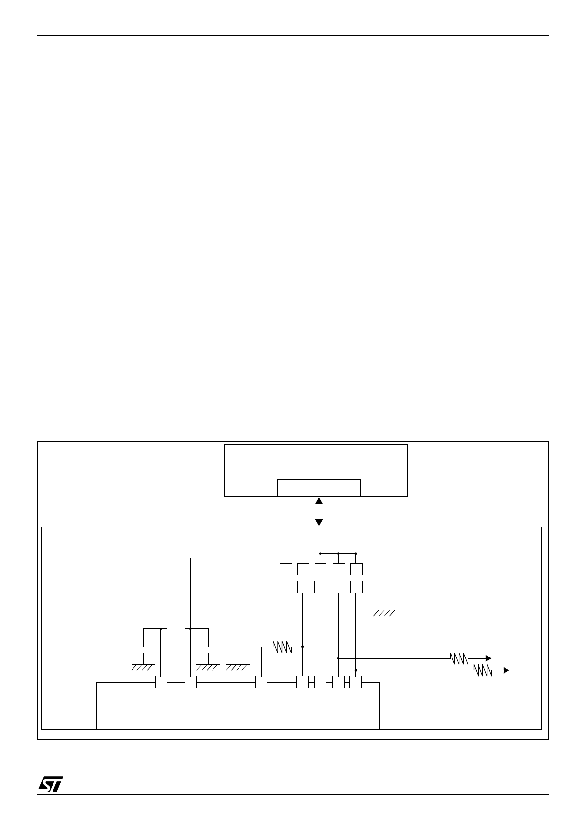
1 INTRODUCTION
The ST7SCR and ST7FSCR devices are members of the ST7 microcontroller family designed for
USB applications. All devices are based on a common industry-standard 8-bit core, feat uring an enhanced instruction set.
The ST7SCR ROM devices are factory-programmed and are not reprogrammable.
The ST7FSCR versions feature dual-voltage
Flash memory with Flash Programming capability.
They operate at a 4MHz external oscillator frequency.
Under software control, all devices c an be place d
in WAIT or HALT mode, reducing power consumption when the application is in idle or stand-by
state.
The enhanced instruction set and addressing
modes of the ST7 offer both power and flexibility to
software developers, enabling the design of highly
efficient and compact application code. In addition
to standard 8-bit data management, all ST7 microcontrollers feature true bit manipulation, 8x8 un-
signed multiplication and indirect addressing
modes.
The devices include an ST7 Core, up to 16 Kbytes
of program memory, up to 512 bytes of user RAM,
up to 35 I/O lines and the following on-chip peripherals:
– USB full speed interface with 7 endpoints, pro-
grammable in/out configuration and embedded
3.3V voltage regulator and transceivers (no external components are needed).
– ISO7 816-3 UA RT interface with Programmable
Baud rate from 372 clock pulses up to 11.625
clock pulses
– Smartcard Supply Block able to provide pro-
grammable supply voltage and I/O voltage levels
to the smartcards
– Low voltage reset ensuring proper power-on or
power-off of the device (selectable by option)
– Watc hdog Timer
– 8-bit Timer (TBU)
Figure 1. ST7SCR Block Diagram
8-BIT CO RE
ALU
ADDRESS AND DATA BUS
OSCIN
OSCOUT
PA6
4MHz
CONTROL
RAM
(512 Bytes)
PROGRAM
(16K Byt es)
MEMORY
8-BIT TIMER
LVD
V
PP
USBDP
USBDM
USBVCC
PORT C
PC[7:0]
PB[7:0]
PA[5:0]
SUPPLY
MANAG E R
PLL
OSCILLATOR
USB
PORT B
PORT A
USB
DATA
BUFFER
(256 bytes)
DIVIDER
8 MHz
3V/1.8V Vreg
DC/DC
CRDDET
CRDIO
CRDC4
CRDC8
CRDRST
CRDCLK
PD[7:0]
ISO7816 UART
PORT D
CONVERTER
CRDVCC
SELF
WATCHDOG
LED
LED[3:0]
or 4 MHz
48 MHz
DIODE
1
ST7SCR
5/102
2 PIN DESCRIPTION
Figure 2. 64-Pin TQFP Package Pinout
WAKUP2/PA2
WAKUP2/PA3
PD0
PD1
PD2
PD3
PD4
PD5
PD6
PD7
OSCIN
OSCOUT
CRDDET
VDD
WAKUP2/ICCDATA/PA0
WAKUP2/ICCCLK/PA1
64 63 62 61 6 0 59 58 57 56 55 54 53 52 51 50 49
48
47
46
45
44
43
42
41
40
39
38
37
36
35
34
33
17 18 19 20 21 22 23 24 29 30 31 3225 26 27 28
1
2
3
4
5
6
7
8
9
10
11
12
13
14
15
16
C4
CRDIO
C8
GND
PB0
PB1
PB2
PB3
PB4
PB5
PB6
PB7
NC
CRDCLK
NC
PA6
V
PP
PC7/WAKUP1
PC6/WAKUP1
PC5/WAKUP1
PC4/WAKUP1
PC3/WAKUP1
PC2/WAKUP1
PC1/WAKUP1
PC0/WAKUP1
GND
VDD
NC
DP
DM
LED0
SELF1
SELF2
PA5
PA4NCNC
LED3
LED2
LED1
VDD
VDDA
USBVcc
CRDVCC
GND
GNDA
DIODE
CRDRST
NC = Not Connected
1
ST7SCR
6/102
PIN DESCRIPTION (Cont’d)
Figure 3. 24-Pin SO Package Pinout
14
13
11
12
15
16
17
18
LED0
DM
DP
USBVcc
OSCIN
OSCOUT
V
PP
1
2
3
4
5
6
7
8
9
10
DIODE
CRDCLK
CRDRST
CRDVCC
PA6
CRDIO
19
20
C8
CRDDET
ICCDATA/WAKUP2/PA0
V
DDA
C4
GNDA
ICCCLK/WAKUP2/PA1
NC
GND
21
22
23
24
V
DD
SELF
1
ST7SCR
7/102
PIN DESCRIPTION (Cont’d)
Legend / Abbreviations:
Type: I = input, O = output, S = supply
In/Output level: C
T
= CMOS 0.3VDD/0.7VDD with
input trigger
Output level: HS = 10mA high sink (on N-buffer
only)
Port and control configuration:
– Input:float = floating, wpu = weak pull-up, int = in-
terrupt, ana = analog
– Output : OD = open drain, PP = push-pull
Refer to “I/O PORTS” on page 30 for more det ails
on the software configuration of the I/O ports.
Table 1. Pin Description
Pin n°
Pin Name
Type
Level
V
CARD
supplied
Port / Control
Main
Function
(after reset)
Alternate Function
TQFP64
SO24
Input
Output
Input Output
wpu
int
OD
PP
1 5 CRDRST O CTX X Smartcard Reset
2 NC Not Connected
3 6 CRDCLK O C
T
X X Smartcard Clock
4 NC Not Connected
57C4 O C
T
X X Smartcard C4
6 8 CRDIO I/O C
T
X X X Smartcard I/O
79C8 O C
T
X X Smartcard C8
8 3 GND S Ground
9 PB0 O C
T
X X Port B0
1)
10 PB1 O C
T
X X Port B1
1)
11 PB2 O C
T
X X Port B2
1)
12 PB3 O C
T
X X Port B3
1)
13 PB4 O C
T
X X Port B4
1)
14 PB5 O C
T
X X Port B5
1)
15 PB6 O C
T
X X Port B6
1)
16 PB7 O C
T
X X Port B7
1)
17 10 CRDDET I C
T
X Smartcard Detection
18 VDD S Power Supply voltage 4V-5.5V
19 11
PA0/WAKUP2/
ICCDATA
I/O C
T
X X X X Port A0
Interrupt, In-Circuit Communication
Data Input
20 12
PA1/WAKUP2/
ICCCLK
I/O C
T
X X X X Port A1
Interrupt, In-Circuit Communication
Clock Input
21 PA2/WAKUP2 I/O C
T
X X X X Port A2
1)
Interrupt
22 PA3/WAKUP2 I/O C
T
X X X X Port A3
1)
Interrupt
23 PD0 O C
T
X X Port D0
1)
24 PD1 O C
T
X X Port D1
1)
25 PD2 O C
T
X X Port D2
1)
1
ST7SCR
8/102
26 PD3 O C
T
X X Port D3
1)
27 PD4 O C
T
X X Port D4
1)
28 PD5 O C
T
X X Port D5
1)
29 PD6 O C
T
X X Port D6
1)
30 PD7 O C
T
X X Port D7
1)
31 14 OSCIN C
T
Input/Output Oscillator pins. These pins connect a
4MHz parallel-resonant crystal, or an external source
to the on-chip oscillator.
32 15 OSCOUT C
T
33 VDD S Power Supply voltage 4V-5.5V
34 GND S Ground
35 PC0/WAKUP1 I C
T
X X PC0
1)
External interrupt
36 PC1/WAKUP1 I C
T
X X PC1
1)
External interrupt
37 PC2/WAKUP1 I C
T
X X PC2
1)
External interrupt
38 PC3/WAKUP1 I C
T
X X PC3
1)
External interrupt
39 PC4/WAKUP1 I C
T
X X PC4
1)
External interrupt
40 PC5/WAKUP1 I C
T
X X PC5
1)
External interrupt
41 PC6/WAKUP1 I C
T
X X PC6
1)
External interrupt
42 PC7/WAKUP1 I C
T
X X PC7
1)
External interrupt
43 16 V
PP
S
Flash programming voltage. Must be held low in normal operating mode.
44 17 PA6 I C
T
PA6
45 18 LED0 O HS X Constant Current Output
46 19 DM I/O C
T
USB Data Minus line
47 20 DP I/O C
T
USB Data Plus line
48 NC Not Connected
49 21 USBVCC O C
T
3.3 V Output for USB
50 22 V
DDA
S power Supply voltage 4V-5.5V
51 23 V
DD
S power Supply voltage 4V-5.5V
52 LED1 O HS X Constant Current Output
53 LED2 O HS X Constant Current Output
54 LED3 O HS X Constant Current Output
55 NC Not Connected
56 NC Not Connected
57 PA4 I/O C
T
X X X X Port A4
Pin n°
Pin Name
Type
Level
V
CARD
supplied
Port / Control
Main
Function
(after reset)
Alternate Function
TQFP64
SO24
Input
Output
Input Output
wpu
int
OD
PP
1
ST7SCR
9/102
Note 1 : Keyboard interface
58 PA5 I/O C
T
X X X X Port A5
59 24 SELF2 O C
T
An External inductance must be connected to these
pins for the step up converter (refer to Figure 4 to
choose the right capacitance)
60 24 SELF1 O C
T
61 1 DIODE S C
T
An External diode must be connected to this pin for
the step up converter (refer to Figure 4 to choose the
right component)
62 2 GNDA S
Ground
63 3 GND S
64 4 CDRVCC O C
T
X Smartcard Supply pin
Pin n°
Pin Name
Type
Level
V
CARD
supplied
Port / Control
Main
Function
(after reset)
Alternate Function
TQFP64
SO24
Input
Output
Input Output
wpu
int
OD
PP
ST7SCR
10/102
PIN DESCRIPTION (Cont’d)
Figure 4. Smartcard Interface Reference A pplication
Note 1: Refer to Section 6 on page 20.
LED0
DM
DP
USBVcc
OSCIN
OSCOUT
V
PP
DIODE
CRDCLK
CRDRST
CRDVCC
PA6
CRDIO
C8
CRDDET
PA0
V
DDA
C4
GNDA
PA1
NC
GND
V
DD
SELF
V
DD
C
L1
C
L2
C7
C8
C9
V
DD
L1
C5
D1
R
LED
C4
VBUS
D-
D+
GND
SHIELD
C2C1 C3
C6
V
DD
V
DD
D+
D-
Mandatory values for the external components :
C2 : 4.7 µF,ESR 0. 5 Ohm
L1 : 10 µH, 2 Ohm
C7 : 4.7 µF,ESR 0.5 Ohm
C5 : 1 nF
Crystal 4.0 MHz, Impedance m ax100 Ohm
Cl1 , C l2
1)
D1: BAT42 SHOTTKY
C6 : 10 0 nF
C8 : 470 pF
C9 :
100 pF
C1 : 100nF
C3 : 1 µF
C4 : 4.7 µF
R : 1.5kOhm
1
ST7SCR
11/102
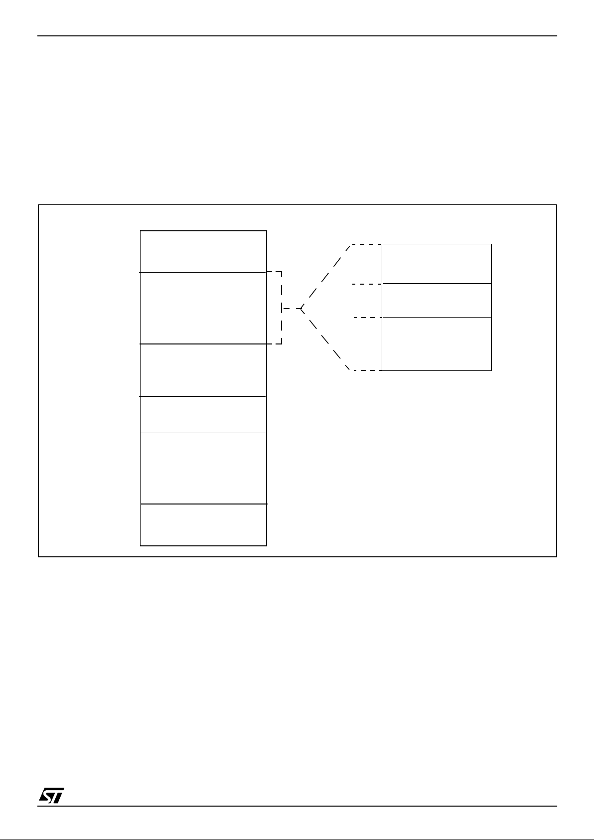
3 REGISTER & MEMORY MAP
As sho wn i n Figure 5, the MCU is capable of ad-
dressing 64K bytes of memories and I/O registers.
The available memory locations consist of 40
bytes of register locations, up to 512 bytes of RAM
and up to 16K bytes of user program memory. The
RAM space includes u p to 128 by t es fo r the stack
from 0100h to 017Fh.
The highest address bytes contain the user re set
and interrupt vectors.
IMPORTANT: Memory locations noted “Reserved” must ne ver be accessed. Ac cessing a reserved area can have unpredictable effects on the
device.
Figure 5. Me m ory M a p
0000h
Interrupt & Reset Vectors
HW Registers
0040h
003Fh
(see Table 2)
FFDFh
FFE0h
FFFFh
(see Table 7)
C000h
033Fh
Program Memory
RAM
USB RAM
(16K Bytes)
Short Addressing
Stack (128 Bytes)
0100h
0180h
023Fh
0040h
00FFh
017Fh
16-bit Addressing RAM
RAM (192 Bytes)
( 192 Bytes)
023Fh
0240h
256 Bytes
(512 Bytes)
Unused
1

ST7SCR
12/102
Table 2. Hardware Regist er Memo ry Ma p
Address Block
Register
Label
Register
name
Reset Status Remarks
0000h
0001h
0002h
0003h
0004h
0005h
0006h
0007h
0008h
0009h
000Ah
000Bh
000Ch
000Dh
CRD
CRDCR
CRDSR
CRDCCR
CRDETU1
CRDETU0
CRDGT1
CRDGT0
CRDWT2
CRDWT1
CRDWT0
CRDIER
CRDIPR
CRDTXB
CRDRXB
Smartcard Interface Control Register
Smartcard Interface Status Register
Smartcard Contact Control Register
Smartcard Elementary Time Unit 1
Smartcard Elementary Time Unit 0
Smartcard Guard time 1
Smartcard Guard time 0
Smartcard Character Waiting Time 2
Smartcard Character Waiting Time 1
Smartcard Character Waiting Time 0
Smartcard Interrupt Enable Register
Smartcard Interrupt Pending Register
Smartcard Transmit Buffer Register
Smartcard Receive Buffer Register
00h
80h
xxh
01h
74h
00h
0Ch
00h
25h
80h
00h
00h
00h
00h
R/W
R/W
R/W
R/W
R/W
R/W
R/W
R/W
R/W
R/W
R/W
R
R/W
R
000Eh Watchdog WDGCR Watchdog Control Register 00h R/W
0011h
0012h
0013h
0014h
Port A
PADR
PADDR
PAOR
PAPUCR
Port A Data Register
Port A Data Direction Register
Option Register
Pull up Control Register
00h
00h
00h
00h
R/W
R/W
R/W
R/W
0015h
0016h
0017h
Port B
PBDR
PBOR
PBPUCR
Port B Data Register
Option Register
Pull up Control Register
00h
00h
00h
R/W
R/W
R/W
0018h Port C PCDR Port C Data Register 00h R/W
0019h
001Ah
001Bh
Port D
PDDR
PDOR
PDPUCR
Port D Data Register
Option Register
Pull up Control Register
00h
00h
00h
R/W
R/W
R/W
001Ch
001Dh
001Eh
001Fh
MISC
MISCR1
MISCR2
MISCR3
MISCR4
Miscellaneous Register 1
Miscellaneous Register 2
Miscellaneous Register 3
Miscellaneous Register 4
00h
00h
00h
00h
R/W
R/W
R/W
R/W
1

ST7SCR
13/102
0020h
0021h
0022h
0023h
0024h
0025h
0026h
0027h
0028h
0029h
002Ah
002Bh
002Ch
002Dh
002Eh
002Fh
0030h
0031h
0032h
0033h
0034h
USB
USBISTR
USBIMR
USBCTLR
DADDR
USBSR
EPOR
CNT0RXR
CNT0TXR
EP1TXR
CNT1TXR
EP2RXR
CNT2RXR
EP2TXR
CNT2TXR
EP3TXR
CNT3TXR
EP4TXR
CNT4TXR
EP5TXR
CNT5TXR
ERRSR
USB Interrupt Status Register
USB Interrupt Mask Register
USB Control Register
Device Address Register
USB Status Register
Endpoint 0 Register
EP 0 ReceptionCounter Register
EP 0 Transmission Counter Register
EP 1 Transmission Register
EP 1 Transmission Counter Register
EP 2 Reception Register
EP 2 Reception Counter Register
EP 2 Transmission Register
EP 2 Transmission Counter Register
EP 3 Transmission Register
EP 3 Transmission Counter Register
EP 4 Transmission Register
EP 4 Transmission Counter Register
EP 5 Transmission Register
EP 5 Transmission Counter Register
Error Status Register
00h
00h
06h
00h
00h
0xh
00h
00h
00h
00h
00h
0xh
00h
00h
00h
00h
00h
00h
00h
00h
00h
R/W
R/W
R/W
R/W
R/W
R/W
R/W
R/W
R/W
R/W
R/W
R/W
R/W
R/W
R/W
R/W
R/W
R/W
R/W
R/W
R/W
0035h
0036h
TBU
TBUCV
TBUCSR
Timer counter value
Timer control status
00h
00h
R/W
R/W
0037h
0038h
0039h
003Ah
ITC
ITSPR0
ITSPR1
ITSPR2
ITSPR3
Interrupt Software Priority Register 0
Interrupt Software Priority Register 1
Interrupt Software Priority Register 2
Interrupt Software Priority Register 3
FFh
FFh
FFh
FFh
R/W
R/W
R/W
R/W
003Bh Flash FCSR Flash Control Status Register 00h R/W
003Eh LED_CTRL LED Control Register 00h R/W
Address Block
Register
Label
Register
name
Reset Status Remarks
1
ST7SCR
14/102
4 FLASH PROGRAM MEMORY
4.1 Introduction
The ST7 dual voltage High Density Flash (HDFlash) is a non-volatile memory that can be electrically erased as a single block or by individual sectors and programmed on a Byte-by-Byte basis using an external V
PP
supply.
The HDFlash devices can be programmed and
erased off-board (plugge d in a programm ing tool)
or on-board using ICP (In-Circuit Programming) or
IAP (In-Application Programming).
The array matrix organ isation allows each sector
to be erased and reprogramm ed without affecting
other sectors.
4.2 Main Features
■ Three Flash programming modes :
– Insertion in a programming tool. In this m ode,
all sectors including option bytes can be programmed or erased.
– ICP (In-Circuit Programming). In this mode, all
sectors including option bytes can be programmed or erased without removing the device from the application board.
– IAP (In-Application Programming) In this
mode, all sectors except Sector 0, can be programmed or erased without removing the device from the application board a nd wh ile the
application is running.
■ ICT (In-Circuit Testing) for downloading and
executing user application test patterns in RAM
■ Read-out protection against piracy
■ Register Access Security System (RASS) to
prevent accidental programming or erasing
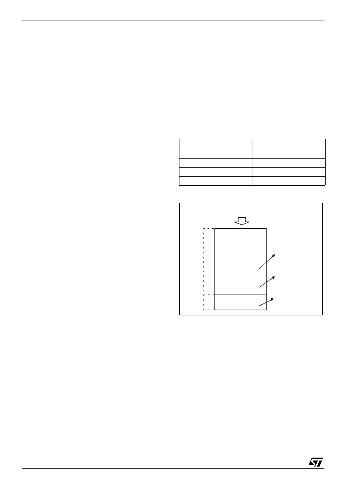
4. 3 S truct u re
The Flash memory is organised in sectors and can
be used for both code and data storage.
Depending on the overall FLASH memory size i n
the microcontroller device, there are up to three
user sectors (see Table 3). Each of these sec tors
can be erased independently to avoid unnecessary erasing of the whole Flash memory when only
a partial erasing is required.
The first two sectors have a fixed siz e of 4 Kby tes
(see Figure 6). They are mapped in the upper part
of the ST7 addressing space so t he reset and interrupt vectors are located in Sector 0 (F000hFFFFh).
Table 3. Sectors available in FLASH devices
Figure 6. Memory map and sector address
Flash Memory Size
(bytes)
Available Sectors
4K Sector 0
8K Sectors 0,1
> 8K Sectors 0,1, 2
4 Kbytes
4 Kbytes
SECTOR 1
SECTOR 0
SECTOR 2
16K USER FLASH MEMORY SIZE
FFFFh
F000h
EFFFh
E000h
DFFFh
C000h
8Kbytes
ex.: user program
ex.: user data
ex.: user system library
+ IAP BootLoader
+ libra ry
1
ST7SCR
15/102
FLASH PROGRAM MEMORY (Cont’d)
4.4 ICP (In-Circuit Programming)
To perform ICP the microcontroller must be
switched to ICC (In-Circuit Communication) mode
by an external controller or programming tool.
Depending on the ICP code dow nloaded in RAM,
Flash memory programming can be fully customized (number of bytes to prog ram, program locations, or selection serial communication interface
for downloading).
When using an STMicroelectronics or third-party
programming tool that supp orts ICP and the specific microcontroller device, the user needs only to
implement the ICP hardware interface on the application board (see Figure 7). For more details on
the pin locations, refer to the device pinout description.
ICP needs six signals to be connec ted to the programming tool. These signals are:
–V
SS
: device power supply ground
–V
DD
: for re s e t by LV D
– OSCIN: to force the clock during power-up
– ICCCLK: ICC output serial clock pin
– ICCDATA: ICC input serial data pin
–V
PP
: ICC mode selection and programming
voltage.
If ICCCLK or ICCDATA are used for other purposes in the application, a serial resistor has to be implemented to avoid a conflict in case one of the
other devices forces the signal level.
Note: To develop a c usto m program mi ng tool, refer to the ST7 FLASH Programmin g and I CC Re ference Manual which gives full details on the ICC
protocol hardware and software.
4.5 IAP (In-Application Programming)
This mode uses a BootLoader program previously
stored in Sector 0 by the user (in ICP mode or by
plugging the device in a programming tool).
This mode is fully controlled by user software. This
allows it to be adapted to the user application, (user-defined strategy for entering programming
mode, choice of communications protocol us ed to
fetch the data to be stored, etc.). For example, it is
possible to download code from the USB interface
and program it in the Flash. IAP mode can be used
to program any of the Flash sectors except Sector
0, which is write/erase protected to allow recovery
in case errors occur during the programming operation.
Figure 7. Typical ICP Interface
ICP PROGRAMMING TOOL CONNECTOR
10k
Ω
C
L2
C
L1
ICCDATA
ICCCLK
V
SS
V
PP
OSCIN
OSCOUT
ST7
HE10 CONNECTOR TYPE
T
OT
HE A
PP
L
ICA
TION
V
DD
4.7k
Ω
APPLICATION BOARD
1
246810
975 3
PROGRAMMING TOOL
ICC CONNECTOR
ICC C a ble
1

ST7SCR
16/102
FLASH PROGRAM MEMORY (Cont’d)
Note: If the ICCCLK or ICCDATA pins are only
used as outputs in the application, no signal isolation is necessary. As soon as the Programming
Tool is plugged to the boa rd, even if an ICC session is not in progress, the ICCCLK and ICCDATA
pins are not available for the application. If they
are used as inputs by the application, isolation
such as a serial resistor has to implemented in
case another device forces the signal. Refer to the
Programming Tool documentation for recommended resistor values.
4.6 Program Memo ry Read-out P rotection
The read-out protection is enabled through an option bit.
For Flash devices, when this option is selected,
the program and data stored in the F lash m em ory
are protected ag ainst rea d-out piracy (i ncluding a
re-write protection). When this protection is removed by reprogramming the Option Byte, the en-
tire Flash program memory is first automatically
erased.
Refer to the Option By te description for more details.
4.6.1 Register Description
FLASH CONTROL/STATUS REGISTER (FCSR)
Read/Write
Reset Value: 0000 0000 (00h)
This register is reserved for use by Programming
Tool software. It controls the FLASH programming
and erasing operations. For details on customizing
FLASH programming methods and In-Circuit Testing, refer to the ST7 FLASH Programming and
ICC Reference Manual.
70
00000000
1
ST7SCR
17/102
5 CENTRAL PRO CESSING UNIT
5.1 INTRODUCTION
This CPU has a full 8-bit architecture and contains
six internal registers allowing efficient 8-bit data
manipulation.
5.2 MAIN FEATURES
■ Enable executing 63 basic instructions
■ Fast 8-bit by 8-bit multiply
■ 17 main addressing modes (with indirect
addressing mode)
■ Two 8-bit index registers
■ 16-bit stack pointer
■ Low power HALT and WAIT modes
■ Priority maskable hardware interrupts
■ Non-maskable software/hardware interrupts
5.3 CPU REGISTERS
The 6 CPU registers shown in Figure 8 are not
present in the memory mapping and are accessed
by spec ifi c ins t ru c tio n s .
Accumulator (A)
The Accumulator is an 8-bit general purpose register used to hold operands and the res ults of the
arithmetic and logic calculations and to manipulate
data.
Index Registers (X and Y)
These 8-bit registers are used to create effective
addresses or as tempo rary storage areas f or data
manipulation. (The Cross -Assembler generates a
precede instruction (PRE) to indicate that the following instruction refers to the Y register.)
The Y register is not affected by the interrupt automatic procedures.
Program Counter (PC)
The program counter is a 16-bit register containing
the address of the next instruction to be executed
by the CPU. It is made of two 8-bit registers PCL
(Program Counter Low which is the LSB) and PCH
(Program Counter High which is the MSB).
Figure 8. CPU Registers
ACCUMULA TOR
X INDEX REGISTER
Y INDEX REGISTER
STACK POINTER
CONDITION CODE REGISTER
PROGRAM COUNTER
70
1C1I1HI0NZ
RESET VALUE = RESET VECTOR @ FFFEh-FFFFh
70
70
70
0
7
15 8
PCH
PCL
15
8
70
RESET VALUE = STACK HIGHER ADDRESS
RESET VALUE =
1X11X1XX
RESET VALUE = XXh
RESET VALUE = XXh
RESET VALUE = XXh
X = Undefined Value
1
ST7SCR
18/102
CENTRAL PROC ESSING UNIT (Cont’d)
Condition Code Reg ister (CC)
Read/Write
Reset Value: 111x1xxx
The 8-bit Condition Code regist er contains the i nterrupt masks and four flags representative of the
result of the instruction just executed. This register
can also be handled by the PUSH and POP instructions.
These bits can be individually tested and/or controlled by specific instructions.
Arithmetic Management Bits
Bit 4 = H
Half carry
.
This bit is set by hardware when a carry occurs between bits 3 and 4 of t he ALU during an ADD or
ADC instructions. It is reset by hardware during
the same instructio n s.
0: No half carry has occurred.
1: A half carry has occurred.
This bit is tested using the JRH or JRNH in struction. The H bit is useful in BCD arithmetic subroutine s .
Bit 2 = N
Negative
.
This bit is set and cleared by hardware. It is representative of the result sign of the last arithmetic,
logical or data manipulation. I t’s a copy of the result 7
th
bit.
0: The result of the last operation is positive or null.
1: The result of the last operation is negative
(i.e. the most significant bit is a logic 1).
This bit is accesse d by the JRMI and JRPL instructions.
Bit 1 = Z
Zero
.
This bit is set and cleared by hardware. This bit indicates that the result of the last arithme tic, logical
or data manipulation is zero.
0: The result of the last operation is dif ferent from
zero.
1: The result of the last operation is zero.
This bit is accessed by the JREQ and JRNE test
instructions.
Bit 0 = C
Carry/borrow.
This bit is set and cleared b y hardware and software. It indicates an overflow or an un derflow has
occurred during the last arithmetic operation.
0: No overflow or underflow has occurred.
1: An overflow or underflow has occurred.
This bit is driven by th e SCF and RCF instructions
and tested by the JRC and JRNC instructions. It i s
also affected by the “bit test and branch”, shift and
rotate instructions.
Interrupt Managem ent B i ts
Bit 5,3 = I1, I0
Interrupt
The combination of the I1 and I0 bits gives the current interrupt software priority.
These two bits are set/cleared by hardware when
entering in interrupt. The loaded value is given by
the corresponding bits in the interrupt software priority registers (IxSPR). They can be also set/
cleared by software with the RIM, SIM, IRET,
HALT, WFI and PUSH/POP instructions.
See the interrupt management chapter for more
details.
70
11I1HI0NZ
C
Interrupt Software Priorit y I1 I0
Level 0 (main) 1 0
Level 1 0 1
Level 2 0 0
Level 3 (= interrupt disable) 1 1
1
ST7SCR
19/102
CENTRAL PROC ESSING UNIT (Cont’d)
Stack Poi nter (SP)
Read/Write
Reset Value: 017Fh
The Stack Pointer is a 16-bit register which is always pointing to the next free location in the stack.
It is then decremented after data has been pushed
onto the stack and incremented before data is
popped from the stack (see Figure 9).
Since the stack is 256 bytes deep, the 8 most significant bits are forced by hard ware. Following a n
MCU Reset, or after a Reset Stack Pointer instruction (RSP), the Stack Pointer contains its reset value (the SP7 to SP0 bits are set) which is the stack
higher address.
The least significant byte of the Stack Pointer
(called S) can be directly accessed by a LD instruction.
Note: When the lower limit is exceeded, the Stack
Pointer wraps around to the stack upper limit, without indicating the stack overflow. The previously
stored information is then o verwritten and therefore lost. The stack also wraps in case of an underflow.
The stack is used to sav e the return address during a subroutine call and the CPU context during
an interrupt. The user may also directly manipulate
the stack by means of the PUSH and POP instructions. In the case of an interrupt, the PCL is stored
at the first location po inted t o by t he SP. Th en t he
other registers are stored in the next locations as
shown in Figure 9
– When an interrupt is received, the SP is decre-
mented and the context is pushed on the stack.
– On return from interrupt, the SP is incremented
and the context is popped from the stack.
A subroutine call occupies two locations and an interrupt five locat ion s i n the stack ar ea.
Figure 9. Stack Manipulation Example
15 8
00000001
70
SP7 SP6 SP5 SP4 SP3 SP2 SP1
SP0
PCH
PCL
SP
PCH
PCL
SP
PCL
PCH
X
A
CC
PCH
PCL
SP
PCL
PCH
X
A
CC
PCH
PCL
SP
PCL
PCH
X
A
CC
PCH
PCL
SP
SP
Y
CALL
Subroutine
Interrupt
Event
PUSH Y POP Y IRET
RET
or RSP
@ 017Fh
@ 0100h
Stack Higher Address = 017Fh
Stack Lower Address =
0100h
1
ST7SCR
20/102
6 SUPPLY, RESET AND CLOCK MANAGEMENT
6.1 CLOCK SYSTEM
6.1.1 General Description
The MCU accepts either a 4MHz crystal or an external clock signal to drive the internal oscillator.
The internal clock (f
CPU
) is derived from the inter-
nal oscillat o r freq uency (f
OSC
), which is 4 Mhz .
After reset, the internal clock (f
CPU
) is provided by
the internal oscillator (4Mhz frequency).
To activate the 48-MHz clock for the USB inter-
face, the user mus t turn on the PLL by setting the
PLL_ON bit in the MISCR4 register. When the PLL
is locked, the LOCK bit is set by hardware.
The user can then select an internal frequency
(f
CPU
) of either 4 MHz or 8MHz by programming
the CLK_SEL bit in t he MISCR4 register (refer to
MISCELLANEOUS REGISTERS section on page
37).
The PLL provides a signal with a duty cycle of 50
%.
The internal clock signal (f
CPU
) is also routed to
the on-chip peripherals. The CPU clock signal
consists of a square wave with a duty cycle of
50%.
Figure 10. Clock, Reset and Supply Block Diagram
The internal oscillat or is designed to operate with
an AT-cut parallel resonant quartz in the frequency range specified for f
osc
. The circuit shown in
Figure 12 is recommend ed when using a crystal,
and Table 4 lists the recommended capacitance.
The crystal and associated components should be
mounted as close as p ossible to the input pins i n
order to minimize output distortion and start-up
stabilisation time. The LOCK bit in the MISCR4
register can also be used to generat e the f
CPU
di-
rectly from f
OSC
if the PLL and the US B interface
are not active.
Table 4. Recommended Values for 4 MHz
Crystal Resonator
Note: R
SMAX
is the equivalent serial resistor of the
crystal (see crystal specification).
PLL_
MISCR4
ON
-
-
----
LOCK
4 Mhz
INTERNAL
8 Mhz
CLOCK (f
CPU
)
4 MHz
PLL
X 12
48 MHz
USB
48 MHz
DIV
(f
OSC
)
CLK_
SEL
R
SMAX
20
Ω
25
Ω
70
Ω
C
OSCIN
56pF 47pF 22pF
C
OSCOUT
56pF 47pF 22pF
1
ST7SCR
21/102
CLOCK SYSTEM (Cont’d)
6.1.2 External Clock
An external clock may be applied to the OSCIN input with the OSCOUT pin not connected, as
shown on Figure 11.
Figure 11. .External Clock Source Connections
Figure 12. Crystal Resonator
OSCIN OSCOUT
EXTERNAL
CLOCK
NC
OSCIN OSCOUT
C
OSCIN
C
OSCOUT
1
ST7SCR
22/102
6.2 RESET SEQUENCE MANAGER (RSM)
6.2.1 Introd uc tion
The reset sequence manager has two reset sources:
■ Internal LVD reset (Low Voltage Detection)
which includes both a power-on and a voltage
drop reset
■ Internal watchdog reset generated by an
internal watchdog counter unde rflow as shown
in Figure 14.
6.2.2 Functional Description
The reset service routine vector is fixed at addresses FFFEh-FFFFh in the ST7 memory map.
The basic reset sequence consists of 3 phases as
shown in Figure 13:
■ A first delay of 30µs + 127 t
CPU
cycles during
which the internal reset is maintained.
■ A second delay of 512 t
CPU
cycles after the
internal reset is generated. It allows the
oscillator to stabilize and ens ures that recovery
has taken place from the Reset state.
■ Reset vector fe tch (duration: 2 clock cycles)
Low Voltage Detector
The low voltage detector gene rates a reset when
V
DD<VIT+
(rising edge) or VDD<V
IT-
(falling edge),
as shown in Figure 13.
The LVD filters spikes on V
DD
larger than t
g(VDD)
to
avoid para siti c rese ts. Se e “ SUP PLY AND RESET
CHARACTERISTICS” on page 79.
Figure 13. LVD RESET Sequence
Figure 14. Watchd og RESET Seque nce
DELAY 1
RUN
LVD
RESET
FETCH VECTOR (2 t
CPU
)
DELAY 2
LVD
RESET
INTERNAL
RESET
DELAY 1 = 30µs + 127 t
CPU
DELAY 2 = 512 t
CPU
V
DD
V
IT+
V
IT-
WATCHDOG
WATCHDOG UN DE RFL OW
RESET
FETCH VECTOR (2 t
CPU
)
DELAY 1
WATCHDOG
RESET
DELAY 2
DELAY 1 = 30µs + 127 t
CPU
DELAY 2 = 512 t
CPU
RUN
1
ST7SCR
23/102
7 INTERRUP T S
7.1 INTRODUCTION
The ST7 enhanced interrupt management provides the following features:
■ Hardware interrupts
■ Software interrupt (TRAP)
■ Nested or concurrent interrupt management
with flexible interrupt priority and level
management:
– Up to 4 software programmable nesting levels
– Up to 16 interrupt vectors fixed by hardware
– 3 non maskable events: TLI, RESET, TRAP
This interrupt management is based on:
– Bit 5 and bit 3 of the CPU CC register (I1:0),
– Interrupt software priority registers (ISPRx),
– F ixed interrupt vecto r addresses locat ed at the
high addresses of the memory map (FFE0h to
FFFFh) sorted by hardware priority order.
This enhanced interrupt cont roller guarantees full
upward compatibility with the standard (not nested) ST7 interrupt controller.
7.2 MASKI N G AND PRO C ESSING FLOW
The interrupt masking is managed by the I1 and I0
bits of the CC register and the ISPRx registers
which give the interrupt software priority level of
each interrupt vector (see Table 5 ). The processing flow is shown in Figure 15 .
When an interrupt request has to be serviced:
– Normal processing is suspended at the end of
the current instruction execution.
– The PC, X, A and CC registers are saved onto
the stack.
– I1 and I0 bits of CC register are set according to
the corresponding values in the ISPRx registers
of the serviced interrupt vector.
– The PC is then loaded with the interrupt vector of
the interrupt to service and the first instruction of
the interrupt service routine is fetched (refer to
“Interrupt Mapping” table for vector addresses).
The interrupt service routine should end with the
IRET instruction which c auses the contents of the
saved registers to be recovered from the stack.
Note: As a cons equence of the IRET instruction,
the I1 and I0 bits will be restored from the stack
and the program in the previous level will resume.
Table 5. Interrupt Software Priority Levels
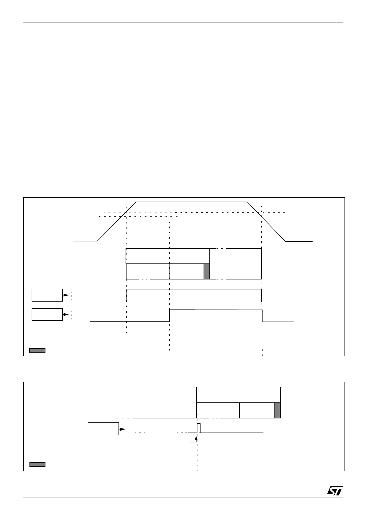
Figure 15. Int errupt Processing Flow c hart
Interrupt software priority Le vel I1 I0
Level 0 (main) Low
High
10
Level 1 0 1
Level 2 0 0
Level 3 (= interrupt disable) 1 1
“IRET”
RESTORE PC, X, A, CC
STACK PC, X, A, CC
LOAD I1:0 FROM INTERR UPT SW REG.
FETCH NEX T
RESET
TLI
PENDING
INSTRUCTION
I1:0
FROM STACK
LOAD PC FROM INTERRUPT VECTOR
Y
N
Y
N
Y
N
Interrupt has the same or a
lower software priority
THE INTERRUPT
STAYS PENDING
than c u rrent one
Interrupt has a higher
softwarepr iority
than current one
EXECUTE
INSTRUCTION
INTERRUPT
1
ST7SCR
24/102
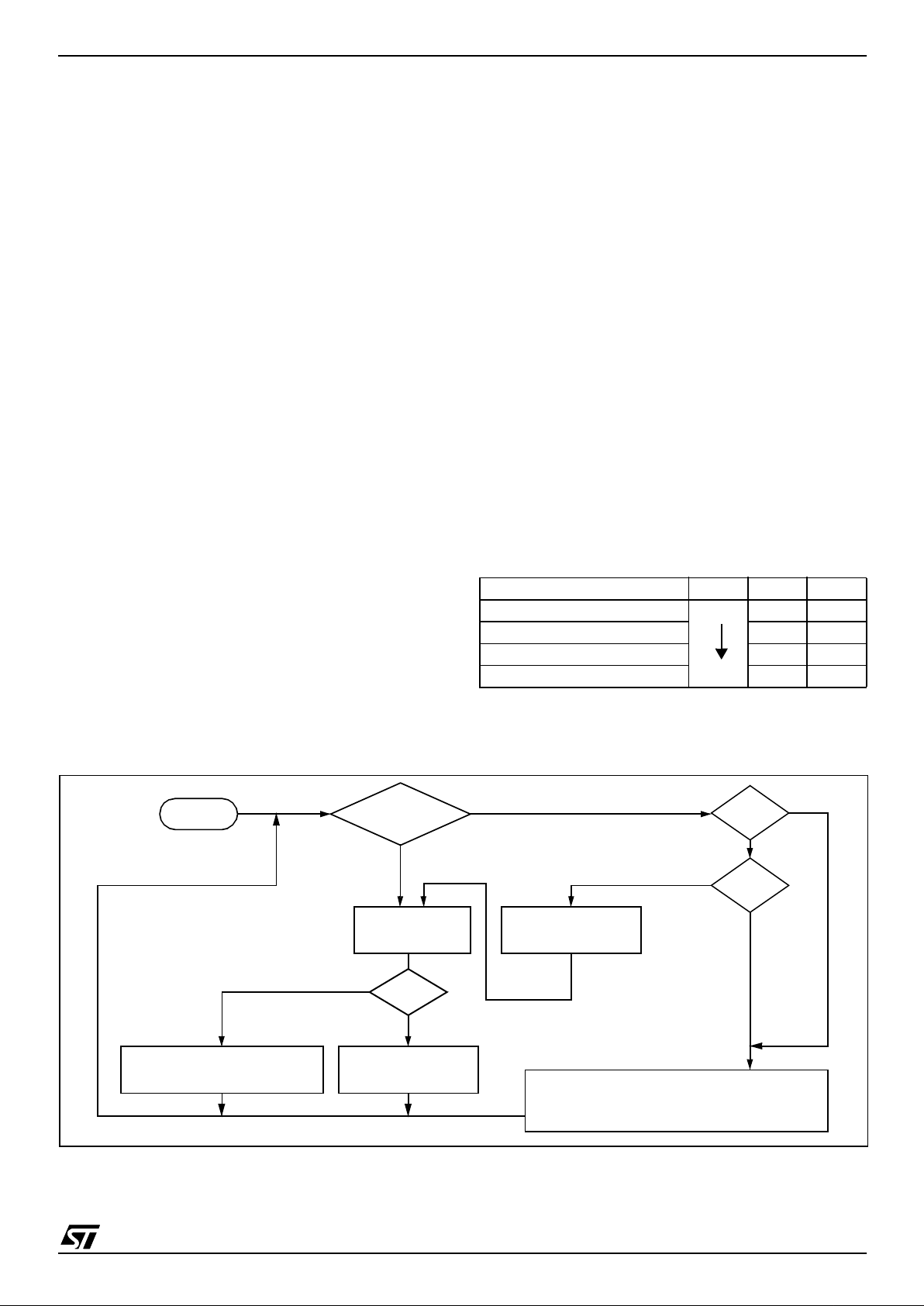
INTERRUPTS (Cont’d)
Servicing Pending In te rrup t s
As several interrupts can b e pen ding at the s ame
time, the interrupt to be taken into account is determined by the following two-step process:
– the highest software priority interrupt is serviced,
– i f several interrupts have the same software pri-
ority then the interrupt with the highest hardware
priority is serviced first.
Figure 16 describes this decision process.
Figure 16. Priority Decision Process
When an interrupt request is not serviced immediately, it is latched and then processed when its
software priority combined with the hardware priority becomes the highest one.
Note 1: The hardware priority is exclusive while
the software one i s not. This allows the prev ious
process to succeed with only one interrupt.
Note 2: RESET, TRAP and TLI are non maskable
and they can be considered as havin g the highest
software priority in the decision process.
Different Interrupt Vector Sources
Two interrupt source types are managed by the
ST7 interrupt controller: the non-maskable type
(RESET, TLI, TRAP) and the maskable type (external or from internal peripherals).
Non-Maskable Sources
These sources are processed regardless of the
state of the I1 and I0 bits of the CC register (see
Figure 15). After stacking the PC, X, A and CC
registers (except for RESET), the corresponding
vector is loaded in the PC register and t he I1 and
I0 bits of the CC are set to disable interrupts (level
3). These sources allow the processor to exit
HALT mode.
■ TLI (Top Level Hardware Interrupt)
This hardware interrupt occurs when a specific
edge is detected on the dedicated TLI pin.
Caution: A TRAP instruction must not be used in a
TLI service routine.
■ TRAP (Non Maskable Software Interrupt)
This software interrupt is serviced when the TRAP
instruction is executed. It will be serviced according to the flowchart in Figure 15 as a TLI.
Caution: TRAP can be interrupted by a TLI.
■ RESET
The RESET source has the highe st priority in the
ST7. This means that the first current routine has
the highest software priority (level 3) and the highest hardware priority.
See the RESET chapter for more details.
Maskable Sources
Maskable interrup t vector sourc es can be servi ced
if the corresponding in terrupt is enabled and if its
own interrupt software priority (in ISPRx registers)
is higher than the one currently being serviced (I1
and I0 in CC register). If any of these two co nditions is false, the interrupt is la tched and thus remains pending.
■ External Interrupts
External interrupts allow the processor to exit from
HALT low power mode.
External interrupt sensitivity is software selectable
through the External Interrupt Control register
(EICR).
External interrupt triggered on edge will be latched
and the interrupt request automatically cleared
upon entering the interrupt service routine.
If several input pins of a group connected to the
same interrupt line are selected simultaneously,
these w ill be log i cally NANDed.
■ Peripheral Interrupts
Usually the peripheral interrupts cause the MCU to
exit from HALT mode except thos e mentioned in
the “Interrupt Mapping” table.
A peripheral interrupt occurs when a specific flag
is set in the peripheral status registers and if the
corresponding enable bit is set in the peripheral
control register.
The general sequence for clearing an interrupt is
based on an access to the status register followed
by a read or write to an associated register.
Note: The clearing sequence resets the internal
latch. A pending interrupt (i.e. waiting for being
serviced) will therefore be lost if the clear sequence is executed.
PENDING
SOFTWARE
Different
INTERRUPTS
Same
HIGHEST HARDWARE
PRIORITY SERVICED
PRIORITY
HIGHEST SOFTWARE
PRIORITY SERVICED
1
ST7SCR
25/102
INTERRUPTS (Cont’d)
7.3 INTERRUPTS AND LOW POWER MODES
All interrupts allow the processor to exit the WAIT
low power mode. On the contrary, only external
and other specified interrupt s allow the processor
to exit from the HALT modes (see column “Exit
from HALT” in “Interrupt Mapping” table). When
several pending interrupts are present whi le exiting HALT mode, the first one serviced can only be
an interrupt with e xit from HALT mode c apability
and it is selected through the same decision proc ess shown in Figure 16.
Note: If an interrupt, that is not able to Exit from
HALT mode, is pending with the highest priority
when exiting HALT mode, this interrupt is serviced
after the first one serviced.
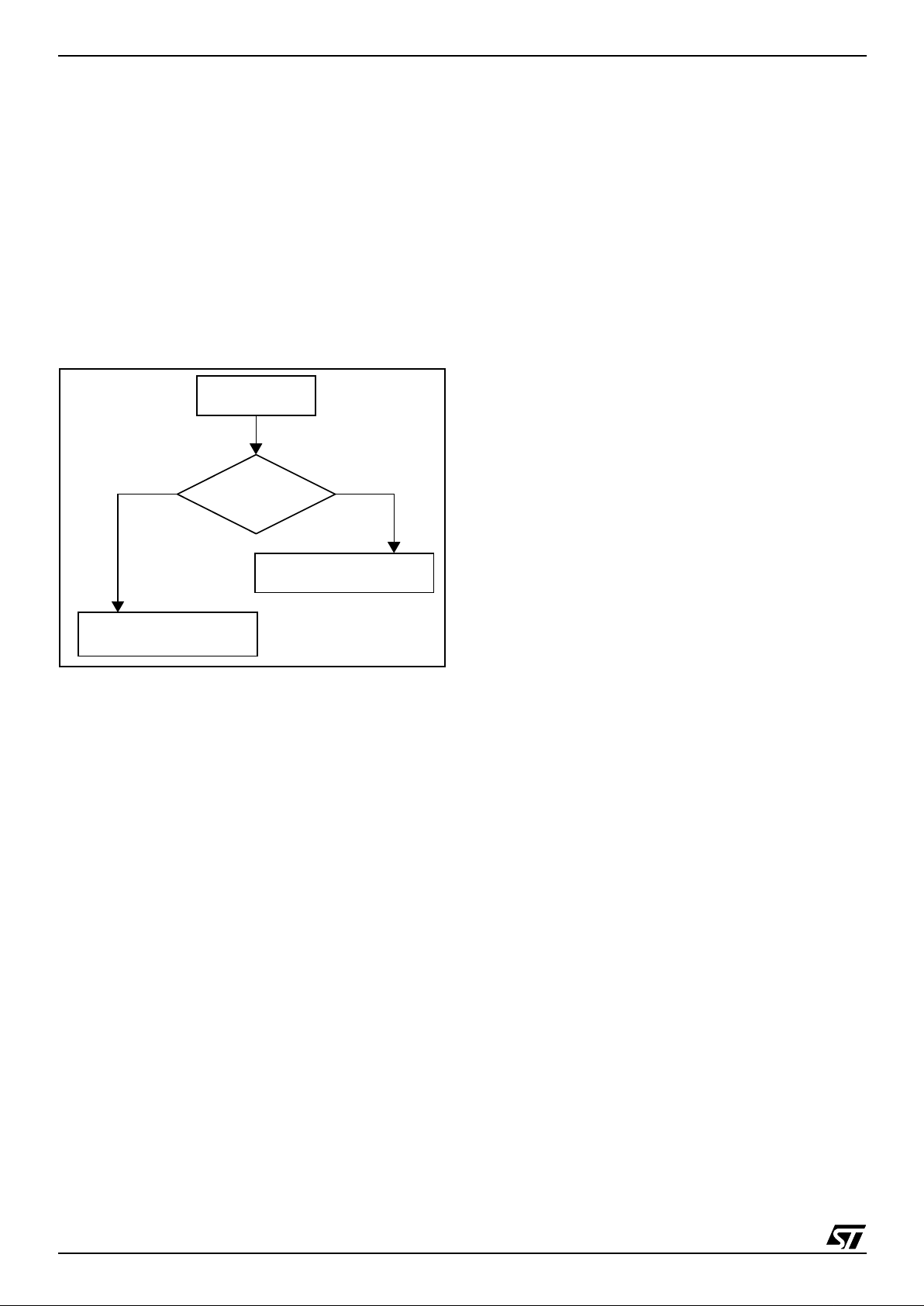
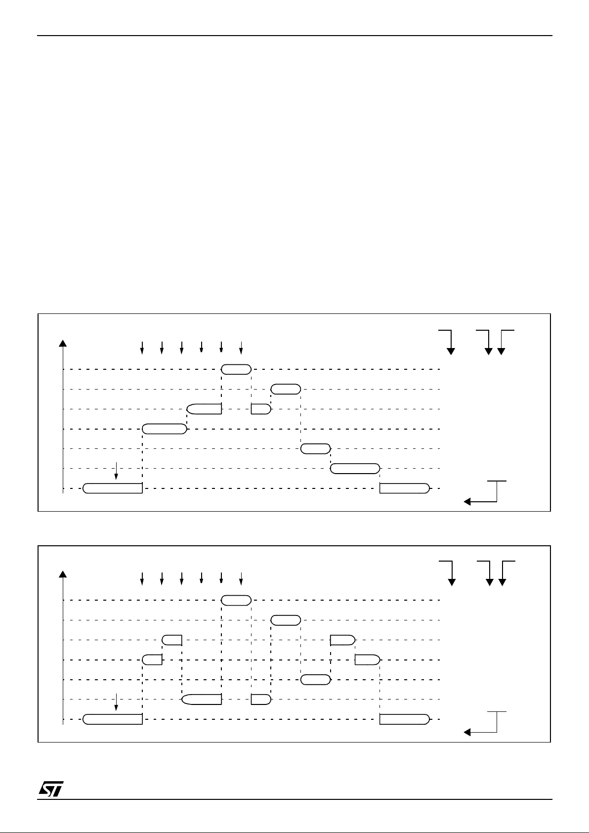
7.4 CONCURRENT & NESTED MANAGEMENT
The following Figure 17 and Figure 18 show two
different interrupt management modes. The first is
called concurrent mode and do es not allow an interrupt to be interrupted, unlike the nested mode in
Figure 18. The interrupt hardware priority is given
in this order from the l owes t to the hi ghest: M A IN,
IT4, IT3 , IT2, IT1, IT0, TLI. The software priority is
given for each interrupt.
Warning: A stack overflow may occur without notifying the software of the failure.
Figure 17. Concurrent Interrupt Managem ent
Figure 18. Nested Interrupt Management
MAIN
IT4
IT2
IT1
TLI
IT1
MAIN
IT0
I1
HARDWARE PRIORITY
SOFTWARE
3
3
3
3
3
3/0
3
11
11
11
11
11
11 / 10
11
RIM
IT2
IT1
IT4
TLI
IT3
IT0
IT3
I0
10
PRIORITY
LEVEL
USED STACK = 10 BYTES
MAIN
IT2
TLI
MAIN
IT0
IT2
IT1
IT4
TLI
IT3
IT0
HARDWARE PRIORITY
3
2
1
3
3
3/0
3
11
00
01
11
11
11
RIM
IT1
IT4
IT4
IT1
IT2
IT3
I1 I0
11 / 10
10
SOFTWARE
PRIORITY
LEVEL
USED STACK = 20 BYTES
1
ST7SCR
26/102
INTERRUPTS (Cont’d)
7.5 INTERRUPT REGISTER DESCRIPTION
CPU CC REGISTER INTERRUPT BITS
Read/Write
Reset Value: 111x 1010 (xAh)
Bit 5, 3 = I1, I0
Soft w a re In te r r u p t Priority
These two bits indicate the current interrupt software priority.
These two bits are set/cle ared by hardware whe n
entering in interrupt. The loaded value is given by
the corresponding bits in the interrupt software priority registers (ISPRx).
They can be also s et/cleared by s oft ware wi th the
RIM, SIM, HALT, WFI, IRET and PUSH/POP instructions (see “Interrupt Dedicated Instruction
Set” table).
*Note: TLI, TRAP and RESET events are non
maskable sources and can interrupt a level 3 program.
INTERRUPT SOFTWARE PRIORITY REGISTERS (ISPRX)
Read/Write (bit 7:4 of ISPR3 are read only)
Reset Value: 1111 1111 (FFh)
These four registers contain the interrupt software
priority of each interrupt vector.
– Each interrupt vector (except RESET and TRAP)
has corresponding bits in these registers where
its own software priority is stored. This correspondance is shown in the following table.
– Each I1_x and I0_x bit value in the ISPRx regis-
ters has the same meaning as the I1 and I0 bits
in the CC register.
– Level 0 can not be written (I1_x=1, I0_x=0). In
this case, the previously stored value is kept. (example: previous=CFh, write=64h, result=44h)
The RESET, TRAP a nd TLI vectors have no s oftware priorities. When one is serviced, the I1 and I0
bits of the CC register are both set.
*Note: Bits in the ISPRx registers which correspond to the TLI can be read and written but they
are not significant in the interrupt process management.
Caution: If the I1_x and I0_x bits are modified
while the interrupt x is execu ted the following behaviour has to be considered: If the interrupt x is
still pending (new interrupt or flag not cleared) and
the new software priority is highe r than the previous one, the interrupt x is re-ent ered. Otherwise,
the software priority stays unchanged up to the
next interrupt request (after the IRET of the interrupt x).
70
11I1 H I0 NZC
Interrupt Software Priority Level I1 I0
Level 0 (main)
Low
High
10
Level 1 0 1
Level 2 0 0
Level 3 (= interrupt disable*) 1 1
70
ISPR0 I1_3 I0_3 I1_2 I0_2 I1_1 I 0_1 I1_0 I0_0
ISPR1 I1_7 I0_7 I1_6 I0_6 I1_5 I 0_5 I1_4 I0_4
ISPR2 I1_11 I0_11 I1_10 I0_10 I1_9 I0_9 I1_8 I0_8
ISPR3 1 1 1 1 I1_13 I0_13 I1_12 I0_12
Vector address ISPRx bits
FFFBh-FFFAh I1_0 and I0_0 bits*
FFF9h-FFF8h I1_1 and I0_1 bits
... ...
FFE1h-FFE0h I1_13 and I0_13 bits
1
ST7SCR
27/102
INTERRUPTS (Cont’d)
Table 6. Dedicated Interrupt Instruc tion Set
Note: During the execut ion of an interrupt routine, the HALT, POPCC, RI M, SIM and WFI instructions
change the current software priority up to the next IRET instruction or one of the previously mentioned
instructions.
In order not to lose the current software priority level, the RIM, SIM, HALT, WFI and POP CC instructions
should never be used in an interrupt routine.
Table 7. I nte rrupt Mapping
Note 1: This interrupt can be used to exit from USB suspend mode.
Instruction New Description Function/Example I1 H I0 N Z C
HALT Entering Halt mode 1 0
IRET Interrupt routine return Pop CC, A, X, PC I1 H I0 N Z C
JRM Jump if I1:0=11 I1:0=11 ?
JRNM Jump if I1:0<>11 I1:0<>11 ?
POP CC Pop CC from the Stack Mem => CC I1 H I0 N Z C
RIM Enable interrupt (level 0 set) Load 10 in I1:0 of CC 1 0
SIM Disable interrupt (level 3 set) Load 11 in I1:0 of CC 1 1
TRAP Software trap Software NMI 1 1
WFI Wait for interrupt 1 0
N°
Source
Block
Description
Register
Label
Priority
Order
Exit
from
HALT
Address
Vector
RESET Reset
N/A
Highest
Priority
Lowest
Priority
yes FFFEh-FFFFh
TRAP Software Interrupt
no
FFFCh-FFFDh
0 ICP FLASH Start programming NMI interrupt FFFAh-FFFBh
1 UART ISO7816-3 UART Interrupt UIC FFF8h-FFF9h
2 USB USB Communication Interrupt USBISTR FFF6h-FFF7h
3 WAKUP1 External Interrupt Port C yes FFF4h-FFF5h
4 WAKUP2 External Interrupt Port A yes FFF2h-FFF3h
5 TIM TBU Timer Interrupt TBUSR no FFF0h-FFF1h
6 CARDDET
1)
Smartcard Insertion/Removal Interrupt
1)
USCUR
yes
FFEEh-FFEFh
7 ESUSP End suspend Interrupt USBISTR FFECh-FFEDh
8 Not used no FFEAh-FFEBh
1
ST7SCR
28/102
8 POWER SAVING MODES
8.1 INTRODUCTION
To give a large measure of flexibility to the application in terms of power consumption, two main power saving modes are implemented in the ST7.
After a RESET the normal operat ing mode is selected by default (RUN mode). This mode drives
the device (CPU and embedded peripherals) by
means of a master clock which is based on the
main oscillator frequency.
From Run mode, the different power saving
modes may be selected by setting the relevant
register bits or by calling the specific ST7 software
instruction whose action depends on the oscillator
status.
8.2 WAIT MODE
WAIT mode places the MCU in a low power c onsumption mode by stopping the CPU.
This pow e r s a v ing mo de is selected by calling the
“WFI” ST7 software instruction.
All peripherals remain active. During WAIT mode,
the I bit of the CC register is forced to 0, to enable
all interrupts. All other registers and memory remain unchanged. The MCU remains in WAIT
mode until an interrupt or Res et oc curs, where upon the Program Counter branches to the starting
address of the interrupt or Reset service routine.
The MCU w ill re mai n in W AIT mo de unt il a Res et
or an Interrupt occurs, causing it to wake up.
Refer to Figure 19.
Figure 19. WAIT Mode Flow Chart
WFI INSTRUCTION
RESET
INTERRUPT
Y
N
N
Y
CPU CLOCK
OSCILLATOR
PERIPH. CLOCK
I-BIT
ON
ON
CLEARED
OFF
CPU CLOCK
OSCILLATOR
PERIPH. CLOCK
I-BIT
ON
ON
SET
ON
FETCH RESET VECTOR
OR SERVICE INTERRUPT
512 CPU CLOCK
CYCLES DELAY
IF RESET
Note: Before servicing an interrupt, the CC
register is pushed on the stack. The I-Bit is set
during the interrupt routine and cleared when
the CC register is popped.
1
ST7SCR
29/102
POWER SAVING MODES (Cont’d)
8.3 HALT MODE
The HALT mode is the MCU lowest power consumption mode. The HALT mode is entered by executing the HALT instruction. The internal oscillator is then turned off, causing all internal processing to be stopped, including the operation of the
on-chip peripherals.
Note: Th e PL L must be disabled before a HALT
instruction.
When entering HALT mode, the I bit in the Condition Code Register is cleared. Thus, any of the external interrupts (ITi or US B end suspend mode),
are allowed and if an interrupt occurs, the CPU
clock becomes active.
The MCU can e xit HAL T mode on reception of either an external interrupt on ITi, an end suspen d
mode interrupt coming from USB peripheral, or a
reset. The osc illato r is t hen t ur ned on and a stabilization time is provided before rele as ing CPU operation. The stabilization time is 512 CPU clock cycles.
After the start up delay, the CPU continues operation by servicing the interrupt which wakes it up or
by fetching the reset vector if a reset wakes it up.
Figure 20. HALT Mod e Flo w C hart
N
N
EXTERNAL
INTERRUPT*
RESET
HALT INSTRUCTION
512 CPU CLOCK
FETCH RESET VECTOR
OR SERVICE INTERRUPT
CYCLES DELAY
CPU CLOCK
OSCILLATOR
PERIPH. CLOCK
I-BIT
ON
ON
SET
ON
CPU CLOCK
OSCILLATOR
PERIPH. CLOCK
I-BIT
OFF
OFF
CLEARED
OFF
Y
Y
Note: Before servicing an interrupt, the CC
register is pushed on the stack. The I-Bit is set
during the interrupt routine and c leared when
the CC register is popped.
1
ST7SCR
30/102
9 I/O PORTS
9.1 Introduction
The I/O ports offer different functional modes:
– transfer of data through digital inputs and outputs
and for specific pins:
– alternate signal input/output for the on-chip pe-
ripherals.
– external interrupt detection
An I/O port i s c om posed of up to 8 pins. E ach pin
can be programmed independently as digital input
(with or without interrupt generation) or digital output.
9.2 Functional description
Each port is associated to 4 main registers:
– Data Register (DR)
– Data Direction Register (DDR)
– Option Register (OR)
– Pull Up Register (PU)
Each I/O pin may be programmed using the corre-
sponding register bits in DDR register: bit X corresponding to pin X of the port. The same correspondence is used for the DR register.
Table 8. I /O Pi n Fu nc ti ons
Input Modes
The input configuration is s ele cted by clearing the
corresponding DDR register bit.
In this case, reading the DR register returns the
digital value applied to the external I/O pin.
Note 1: All the inputs are triggered by a Schmitt
trigg er.
Note 2: When switching from input mode to output
mode, the DR register should be written first to
output the correct value as soon as the port is configured as an output.
Interrupt function
When an I/O is configured in Input with Interrupt,
an event on this I/O can generate an external In-
terrupt request to the CPU. The interrupt sensitivity is given independently according to the description mentioned in the ITRFRE interrupt register.
Each pin can independently generate an I nterrupt
request.
Each external interrupt vecto r is linked to a dedicated group of I/O port pins (see Interrupts section). If more than one input pin is selected sim ultaneously as interrupt source, this is logically
ORed. For this reason if one of the interrupt pins is
tied low, it masks the other ones.
Output Mode
The pin is configured in output mode by setting the
corresponding DDR register bit (see Table 7).
In this mode, writing “0” or “1” to the DR register
applies this digital value to the I/O pin throu gh the
latch. Then reading the DR register returns the
previously stored value.
Note: In thi s mo de, th e interrupt function is disabled.
Digital A lternate Func ti on
When an on-chip peripheral is configured to use a
pin, the alternate function is au tomatically selected. This alternate function takes priority over
standard I/O programming. When the signal is
coming from an on-chip peripheral, the I/O pin is
automatically configured in output mode (push-pull
or open drain according to the peripheral).
When the signal is goi ng t o an on-c hip pe ripheral,
the I/O pin ha s to be configured in input m ode. In
this case, the pin’s state is also digitally reada ble
by addressing the DR register.
Notes:
1. Input pull-up conf iguration can cause a n unexpected value at the input of the alternate peripheral input.
2. When the on-chip peripheral uses a pin as input
and output, this pin must be configured as an input
(DDR = 0).
Warning
: The alternate f uncti on m ust not be acti-
vated as long as the pin is configured as input with
interrupt, in order to avoid generating spurious interrupts.
DDR MODE
0 Input
1 Ou tput
1
 Loading...