

SGS Thomson Microelectronics ST7FLITE09Y0M6, ST7FLITE09Y0B6, ST7FLITE09, ST7FLITE05Y0B6, ST7FLITE05Y0M6 Datasheet
...
8-BIT MCU WITH SINGLE VOLTAGE FLASH MEMORY,
■ Memories
– 1K or 1.5K bytes single voltage Flash Pro-
gram memory with read-out protection, In-Circuit and In-Application Programming (ICP and
IAP). 10K write/erase cycles guaranteed, data
retention: 20 years at 55°C.
– 128 bytes RAM.
– 128 bytes data EEPROM with read-out pro-
tection. 300K write/erase cycles guarant eed,
data retention: 20 years at 55°C.
■ Clock, Re set and Supp ly M a nagement
– 3-level low voltage supervisor (LVD) and aux-
iliary voltage detector (AVD) for safe power-
on/off procedures
– Clock sources: internal 1MHz RC 1% oscilla-
tor or external clock
– PLL x4 or x8 for 4 or 8 MHz internal clock
– Four Power Saving Modes: Halt, Active-Halt,
Wait and Slow
■ Interrupt Management
– 10 interrupt vectors plus TRAP and RESET
– 4 external interrupt lines (on 4 vectors)
■ I/O Ports
– 13 multifunctional bidirectional I/O lines
– 9 alternate function lines
– 6 high sink outputs
■ 2 Timers
– One 8-bit Lite Timer (LT) with prescaler in-
cluding: watchdog, 1 rea ltime base and 1 in-
put capture.
ST7LITE0, ST7SUPERLITE
DATA EEPROM, ADC, TIMERS, SPI
DIP16
SO16
150”
– One 12-bit Auto-reload Timer (AT) with output
compare function and PWM
■ 1 Communication Interface
– SPI synchronous serial interface
■ A/D Converter
– 8-bit resolution for 0 to V
– Fixed gain Op-amp for 11-bit resolution in 0 to
250 mV range (@ 5V V
– 5 input channels
■ Instruction Set
– 8-bit data manipulation
– 63 basic instructions
– 17 main addressing modes
– 8 x 8 unsigned multiply instruction
■ Development Tools
– Full hardware/software development package
DD
DD
)
Device Summary
Features
Program memory - bytes 1K 1K 1.5K 1.5K 1.5K
RAM (stack) - bytes 128 (64) 128 (64) 128 (64) 128 (64) 128 (64)
Data EEPROM - bytes----128
Peripherals
Operati ng S upply 2.4V to 5.5V
CPU Fre quency 1MHz RC 1% + PLLx4/8MHz
Operati ng T em perature -40°C to +85°C
Packages SO16 150”, DIP16
LT Timer w/ Wdg,
AT Timer w/ 1 PWM,
ST7SUPERLITE ST7LITE0
ST7LITES2 ST7LITES5 ST7LITE02 ST7LITE05 ST7LITE09
LT Timer w/ Wdg,
AT Timer w/ 1 PWM, SPI,
8-bit ADC w/ Op-Amp
SPI
LT Timer w/ Wdg,
AT Timer w/ 1 PWM,
SPI, 8-bit ADC
LT Timer w/ Wdg,
AT Timer w/ 1 PWM,
SPI
Rev. 2.4
August 2003 1/122
1

Table of Contents
ST7LITE0, ST7SUPERLITE . . . . . . . . . . . . . . . . . . . . . . . . . . . . . 1
1 INTRODUCTION . . . . . . . . . . . . . . . . . . . . . . . . . . . . . . . . . . . . . . . . . . . . . . . . . . . . . . . . . . . . . . 5
2 PIN DESCRIPTION . . . . . . . . . . . . . . . . . . . . . . . . . . . . . . . . . . . . . . . . . . . . . . . . . . . . . . . . . . . . 6
3 REGISTER & MEMORY MAP . . . . . . . . . . . . . . . . . . . . . . . . . . . . . . . . . . . . . . . . . . . . . . . . . . . . 8
4 FLASH PROGRAM MEMORY . . . . . . . . . . . . . . . . . . . . . . . . . . . . . . . . . . . . . . . . . . . . . . . . . . 12
4.1 INTRODUCTION . . . . . . . . . . . . . . . . . . . . . . . . . . . . . . . . . . . . . . . . . . . . . . . . . . . . . . . 12
4.2 MAIN FEATURES . . . . . . . . . . . . . . . . . . . . . . . . . . . . . . . . . . . . . . . . . . . . . . . . . . . . . . 12
4.3 PROGRAMMING MODES . . . . . . . . . . . . . . . . . . . . . . . . . . . . . . . . . . . . . . . . . . . . . . . . 12
4.4 ICC INTERFACE . . . . . . . . . . . . . . . . . . . . . . . . . . . . . . . . . . . . . . . . . . . . . . . . . . . . . . . 13
4.5 MEMORY PROTECTION . . . . . . . . . . . . . . . . . . . . . . . . . . . . . . . . . . . . . . . . . . . . . . . . 14
4.6 RELATED DOCUMENTATION . . . . . . . . . . . . . . . . . . . . . . . . . . . . . . . . . . . . . . . . . . . . 14
4.7 REGISTER DESCRIPTION . . . . . . . . . . . . . . . . . . . . . . . . . . . . . . . . . . . . . . . . . . . . . . . 14
5 DATA EEPROM . . . . . . . . . . . . . . . . . . . . . . . . . . . . . . . . . . . . . . . . . . . . . . . . . . . . . . . . . . . . . 15
5.1 INTRODUCTION . . . . . . . . . . . . . . . . . . . . . . . . . . . . . . . . . . . . . . . . . . . . . . . . . . . . . . . 15
5.2 MAIN FEATURES . . . . . . . . . . . . . . . . . . . . . . . . . . . . . . . . . . . . . . . . . . . . . . . . . . . . . . 15
5.3 MEMORY ACCESS . . . . . . . . . . . . . . . . . . . . . . . . . . . . . . . . . . . . . . . . . . . . . . . . . . . . . 16
5.4 POWER SAVING MODES . . . . . . . . . . . . . . . . . . . . . . . . . . . . . . . . . . . . . . . . . . . . . . . 18
5.5 ACCESS ERROR HANDLING . . . . . . . . . . . . . . . . . . . . . . . . . . . . . . . . . . . . . . . . . . . . 18
5.6 DATA EEPROM READ-OUT PROTECTION . . . . . . . . . . . . . . . . . . . . . . . . . . . . . . . . . 18
5.7 REGISTER DESCRIPTION . . . . . . . . . . . . . . . . . . . . . . . . . . . . . . . . . . . . . . . . . . . . . . . 19
6 CENTRAL PROCESSING UNIT . . . . . . . . . . . . . . . . . . . . . . . . . . . . . . . . . . . . . . . . . . . . . . . . . 20
6.1 INTRODUCTION . . . . . . . . . . . . . . . . . . . . . . . . . . . . . . . . . . . . . . . . . . . . . . . . . . . . . . . 20
6.2 MAIN FEATURES . . . . . . . . . . . . . . . . . . . . . . . . . . . . . . . . . . . . . . . . . . . . . . . . . . . . . . 20
6.3 CPU REGISTERS . . . . . . . . . . . . . . . . . . . . . . . . . . . . . . . . . . . . . . . . . . . . . . . . . . . . . . 20
7 SUPPLY, RESET AND CLOCK MANAGEMENT . . . . . . . . . . . . . . . . . . . . . . . . . . . . . . . . . . . . 23
7.1 INTERNAL RC OSCILLATOR ADJUSTMENT . . . . . . . . . . . . . . . . . . . . . . . . . . . . . . . . 23
7.2 PHASE LOCKED LOOP . . . . . . . . . . . . . . . . . . . . . . . . . . . . . . . . . . . . . . . . . . . . . . . . . 23
7.3 REGISTER DESCRIPTION . . . . . . . . . . . . . . . . . . . . . . . . . . . . . . . . . . . . . . . . . . . . . . . 24
7.4 RESET SEQUENCE MANAGER (RSM) . . . . . . . . . . . . . . . . . . . . . . . . . . . . . . . . . . . . . 26
7.5 SYSTEM INTEGRITY MANAGEMENT (SI) . . . . . . . . . . . . . . . . . . . . . . . . . . . . . . . . . . 28
8 INTERRUPTS . . . . . . . . . . . . . . . . . . . . . . . . . . . . . . . . . . . . . . . . . . . . . . . . . . . . . . . . . . . . . . . 33
8.1 NON MASKABLE SOFTWARE INTERRUPT . . . . . . . . . . . . . . . . . . . . . . . . . . . . . . . . . 33
8.2 EXTERNAL INTERRUPTS . . . . . . . . . . . . . . . . . . . . . . . . . . . . . . . . . . . . . . . . . . . . . . . 33
8.3 PERIPHERAL INTERRUPTS . . . . . . . . . . . . . . . . . . . . . . . . . . . . . . . . . . . . . . . . . . . . . 33
9 POWER SAVING MODES . . . . . . . . . . . . . . . . . . . . . . . . . . . . . . . . . . . . . . . . . . . . . . . . . . . . . 36
9.1 INTRODUCTION . . . . . . . . . . . . . . . . . . . . . . . . . . . . . . . . . . . . . . . . . . . . . . . . . . . . . . . 36
9.2 SLOW MODE . . . . . . . . . . . . . . . . . . . . . . . . . . . . . . . . . . . . . . . . . . . . . . . . . . . . . . . . . 36
9.3 WAIT MODE . . . . . . . . . . . . . . . . . . . . . . . . . . . . . . . . . . . . . . . . . . . . . . . . . . . . . . . . . . 37
9.4 ACTIVE-HALT AND HALT MODES . . . . . . . . . . . . . . . . . . . . . . . . . . . . . . . . . . . . . . . . 38
122
2/122
2

Table of Contents
10 I/O PORTS . . . . . . . . . . . . . . . . . . . . . . . . . . . . . . . . . . . . . . . . . . . . . . . . . . . . . . . . . . . . . . . . . 41
10.1 INTRODUCTION . . . . . . . . . . . . . . . . . . . . . . . . . . . . . . . . . . . . . . . . . . . . . . . . . . . . . . . 41
10.2 FUNCTIONAL DESCRIPTION . . . . . . . . . . . . . . . . . . . . . . . . . . . . . . . . . . . . . . . . . . . . 41
10.3 UNUSED I/O PINS . . . . . . . . . . . . . . . . . . . . . . . . . . . . . . . . . . . . . . . . . . . . . . . . . . . . . 44
10.4 LOW POWER MODES . . . . . . . . . . . . . . . . . . . . . . . . . . . . . . . . . . . . . . . . . . . . . . . . . . 44
10.5 INTERRUPTS . . . . . . . . . . . . . . . . . . . . . . . . . . . . . . . . . . . . . . . . . . . . . . . . . . . . . . . . . 4 4
10.6 I/O PORT IMPLEMENTATION . . . . . . . . . . . . . . . . . . . . . . . . . . . . . . . . . . . . . . . . . . . . 44
11 ON-CHIP PERIPHERALS . . . . . . . . . . . . . . . . . . . . . . . . . . . . . . . . . . . . . . . . . . . . . . . . . . . . . 46
11.1 LITE TIMER (LT) . . . . . . . . . . . . . . . . . . . . . . . . . . . . . . . . . . . . . . . . . . . . . . . . . . . . . . . 46
11.2 12-BIT AUTORELOAD TIMER (AT) . . . . . . . . . . . . . . . . . . . . . . . . . . . . . . . . . . . . . . . . 51
11.3 SERIAL PERIPHERAL INTERFACE (SPI) . . . . . . . . . . . . . . . . . . . . . . . . . . . . . . . . . . . 57
11.4 8-BIT A/D CONVERTER (ADC) . . . . . . . . . . . . . . . . . . . . . . . . . . . . . . . . . . . . . . . . . . . 68
12 INSTRUCTION SET . . . . . . . . . . . . . . . . . . . . . . . . . . . . . . . . . . . . . . . . . . . . . . . . . . . . . . . . . 72
12.1 ST7 ADDRESSING MODES . . . . . . . . . . . . . . . . . . . . . . . . . . . . . . . . . . . . . . . . . . . . . . 72
12.2 INSTRUCTION GROUPS . . . . . . . . . . . . . . . . . . . . . . . . . . . . . . . . . . . . . . . . . . . . . . . . 75
13 ELECTRICAL CHARACTERISTICS . . . . . . . . . . . . . . . . . . . . . . . . . . . . . . . . . . . . . . . . . . . . . 78
13.1 PARAMETER CONDITIONS . . . . . . . . . . . . . . . . . . . . . . . . . . . . . . . . . . . . . . . . . . . . . . 78
13.2 ABSOLUTE MAXIMUM RATINGS . . . . . . . . . . . . . . . . . . . . . . . . . . . . . . . . . . . . . . . . . 79
13.3 OPERATING CONDITIONS . . . . . . . . . . . . . . . . . . . . . . . . . . . . . . . . . . . . . . . . . . . . . . 80
13.4 SUPPLY CURRENT CHARACTERISTICS . . . . . . . . . . . . . . . . . . . . . . . . . . . . . . . . . . . 86
13.5 CLOCK AND TIMING CHARACTERISTICS . . . . . . . . . . . . . . . . . . . . . . . . . . . . . . . . . . 88
13.6 MEMORY CHARACTERISTICS . . . . . . . . . . . . . . . . . . . . . . . . . . . . . . . . . . . . . . . . . . . 89
13.7 EMC CHARACTERISTICS . . . . . . . . . . . . . . . . . . . . . . . . . . . . . . . . . . . . . . . . . . . . . . . 90
13.8 I/O PORT PIN CHARACTERISTICS . . . . . . . . . . . . . . . . . . . . . . . . . . . . . . . . . . . . . . . . 94
13.9 CONTROL PIN CHARACTERISTICS . . . . . . . . . . . . . . . . . . . . . . . . . . . . . . . . . . . . . . . 99
13.10 COMMUNICATION INTERFACE CHARACTERISTICS . . . . . . . . . . . . . . . . . . . . . . . . 100
13.11 8-BIT ADC CHARACTERISTICS . . . . . . . . . . . . . . . . . . . . . . . . . . . . . . . . . . . . . . . . . 102
14 PACKAGE CHARACTERISTICS . . . . . . . . . . . . . . . . . . . . . . . . . . . . . . . . . . . . . . . . . . . . . . 106
14.1 PACKAGE MECHANICAL DATA . . . . . . . . . . . . . . . . . . . . . . . . . . . . . . . . . . . . . . . . . 106
14.2 THERMAL CHARACTERISTICS . . . . . . . . . . . . . . . . . . . . . . . . . . . . . . . . . . . . . . . . . . 107
14.3 SOLDERING AND GLUEABILITY INFORMATION . . . . . . . . . . . . . . . . . . . . . . . . . . . . 108
15 DEVICE CONFIGURATION AND ORDERING INFORMATION . . . . . . . . . . . . . . . . . . . . . . . 109
15.1 OPTION BYTES . . . . . . . . . . . . . . . . . . . . . . . . . . . . . . . . . . . . . . . . . . . . . . . . . . . . . . 109
15.2 DEVICE ORDERING INFORMATION AND TRANSFER OF CUSTOMER CODE . . . . 111
15.3 DEVELOPMENT TOOLS . . . . . . . . . . . . . . . . . . . . . . . . . . . . . . . . . . . . . . . . . . . . . . . 113
15.4 ST7 APPLICATION NOTES . . . . . . . . . . . . . . . . . . . . . . . . . . . . . . . . . . . . . . . . . . . . . 114
16 IMPORTANT NOTES . . . . . . . . . . . . . . . . . . . . . . . . . . . . . . . . . . . . . . . . . . . . . . . . . . . . . . . 116
16.1 EXECUTION OF BTJX INSTRUCTION . . . . . . . . . . . . . . . . . . . . . . . . . . . . . . . . . . . . 116
16.2 IN-CIRCUIT PROGRAMMING OF DEVICES PREVIOUSLY PROGRAMMED WITH HARDWARE WATCHDOG OPTION 116
16.3 IN-CIRCUIT DEBUGGING WITH HARDWARE WATCHDOG . . . . . . . . . . . . . . . . . . . 116
17 SUMMARY OF CHANGES . . . . . . . . . . . . . . . . . . . . . . . . . . . . . . . . . . . . . . . . . . . . . . . . . . 117
3/122
3

Table of Contents
ERRATA SHEET . . . . . . . . . . . . . . . . . . . . . . . . . . . . . . . . . . . 118
18 SILICON IDENTIFICATION . . . . . . . . . . . . . . . . . . . . . . . . . . . . . . . . . . . . . . . . . . . . . . . . . . . 118
19 REFERENCE SPECIFICATION . . . . . . . . . . . . . . . . . . . . . . . . . . . . . . . . . . . . . . . . . . . . . . . 118
20 SILICON limitations . . . . . . . . . . . . . . . . . . . . . . . . . . . . . . . . . . . . . . . . . . . . . . . . . . . . . . . . 118
20.1 NEGATIVE INJECTION IMPACT ON ADC ACCURACY . . . . . . . . . . . . . . . . . . . . . . . 118
20.2 ADC CONVERSION SPURIOUS RESULTS . . . . . . . . . . . . . . . . . . . . . . . . . . . . . . . . . 119
20.3 FUNCTIONAL ESD SENSITIVITY . . . . . . . . . . . . . . . . . . . . . . . . . . . . . . . . . . . . . . . . 119
21 Device Marking . . . . . . . . . . . . . . . . . . . . . . . . . . . . . . . . . . . . . . . . . . . . . . . . . . . . . . . . . . . . 120
22 ERRATA SHEET REVISION History . . . . . . . . . . . . . . . . . . . . . . . . . . . . . . . . . . . . . . . . . . . 121
To obtain the most recent version of this datasheet,
please check at www.st.com>products>technical literature>datasheet
Please note that an errata sheet can be found at the end of this document on
and pay special attention to the Section “IMPORTANT NOTES” on page 116.
page 118
4/122
1
1 INTRODUCTION
ST7LITE0, ST7SUPERLITE
The ST7LITE0 and ST7SUPERLITE are members
of the ST7 microcontrolle r family. All S T7 devices
are based on a common industry-standard 8-bit
core, featuring an enhanced instruction set.
The ST7LITE0 and ST7SUPERLITE feature
FLASH memory with byte-by-byte In-Circuit Programming (ICP) and In-Application Programming
(IAP) capability.
Under software control, the ST7LITE0 and
ST7SUPERLITE d evices can be plac ed in WAIT,
SLOW, or HALT mode, reducing power consumption when the application is in idle or standby state.
Figure 1. General Block D iagram
Internal
CLOCK
V
V
RESET
DD
SS
1 MHz. RC OSC
+
PLL x 4 or x 8
LVD/AVD
POWER
SUPPLY
CONTROL
The enhanced instruction set and addressing
modes of the ST7 offer both power and flexibility to
software developers, enabling the design of highly
efficient and compact application code. In addition
to standard 8-bit data management, all ST7 microcontrollers feature true bit manipulation, 8x8 unsigned multiplication and indirect addressing
modes.
For easy reference, all parametric data are located
in section 13 on page 78.
LITE TIMER
w/ WATCHDOG
PORT A
ADDRESS AND DATA BUS
12-BIT AUTO-
RELOAD TIMER
PA7:0
(8 bits)
8-BIT CO RE
ALU
FLASH
MEMORY
(1 or 1.5K Byt es)
RAM
(128 Bytes)
DATA EEPROM
(128 Bytes)
SPI
PORT B
8-BIT ADC
PB4:0
(5 bits)
5/122
1
ST7LITE0, ST7SU PERLITE
2 PIN DESCRI PTION
Figure 2. 16-Pin Package Pinout (150mil)
V
SS
V
DD
RESET
SS/AIN0/PB0
SCK/AIN1/P B1
MISO/AIN2/P B2
MOSI/AIN3/P B3
CLKIN/AIN4/P B4
1
2
3
ei3
4
5
6
ei2
7
8
ei0
ei1
PA0 (HS)/LTIC
16
(HS)
PA1
15
PA2
14
13
12
11
10
9
PA3
PA4
PA5
PA6/MCO/ICCC LK
PA7
(HS)/ATPWM0
(HS)
(HS)
(HS)/ICCDATA
(HS) 20mA high sink ca pability
associated external interrupt vect or
ei
x
6/122
1
PIN DESCRIPTION (Cont’d)
Legend / Abbreviations for Tab le 1:
Type: I = input, O = output, S = supply
In/Output level: C= CMOS 0.15V
C
= CMOS 0.3VDD/0.7VDD with input trigger
T
/0.85VDD with input trigger
DD
Output level: HS = 20mA high sink (on N-buffer only)
Port and control configuration:
– Input: float = floating, wpu = weak pull-up, int = interrupt
– Output : OD = open drain
2)
, PP = push-pull
Table 1. Device Pin Description
ST7LITE0, ST7SUPERLITE
1)
, ana = analog
Pin
n°
1V
2V
3 RESET
4 PB0/AIN0/SS
Pin Name
SS
DD
I/O C
Type
S Ground
S Main power supply
I/O C
5 PB1/AIN1/SCK I/O C
6 PB2/AIN2/MISO I/O C
7 PB3/AIN3/MOSI I/O C
8 PB4/AIN4/CLKIN I/O C
9 PA7 I/O C
10 PA6 /MCO/ICCCLK I/O C
PA5/
11
ICCDATA
I/O C
12 PA4 I/O C
13 PA3 I/O C
14 PA2/ATPWM0 I/O C
15 PA1 I/O C
16 PA0/LTIC I/O C
Level Port / Control
Main
Input
T
T
T
T
T
T
T
Input Output
Output
float
int
wpu
OD
ana
X X Top priority non maskable interrupt (active low)
X ei3 X X Port B0
X XXXPort B1 ADC Analog Input 1 or SPI Clock
X XXXPort B2
X ei2 X X Port B3
X XXXPort B4
X ei1 X X Port A7
Function
(after reset)
PP
Alternate Function
ADC Analog Input 0 or SPI Slave
Select (active low)
ADC Analog Input 2 or SPI Master
In/ Slave Out Data
ADC Analog Input 3 or SPI Master
Out / Slave In Data
ADC Analog Input 4 or External
clock input
Main Clock Ou tput/In Circuit Com munication Clock .
Caution: During reset, this pin
X X XXPort A6
T
must be held at high level t o avoid
entering ICC mode unexpectedly
(this is guar anteed by the internal
pull-up if the appl icatio n leav es th e
pin floating).
HS X XXXPort A5 In Circuit Communication Data
T
HS X XXXPort A4
T
HS X XXXPort A3
T
HS X XXXPort A2 Auto-Reload Timer PWM0
T
HS X XXXPort A1
T
HS X ei0 X X Port A0 Lite Timer Input Capture
T
Note:
In the interrupt input column, “ei
” defines the associated external interrupt vector. If the weak pull-up col-
x
umn (wpu) is merged with the interrupt column (int), then the I/O configuration is pull-up interrupt input,
else the configuration is floating interrupt input.
7/122
1
ST7LITE0, ST7SU PERLITE
3 REGISTER & MEMORY MAP
As shown in Figure 3 and Figure 4, the MCU is capable of addressing 64K bytes of memorie s an d I/
O registers.
The available memory locations consist of up to
128 bytes of register locations, 128 bytes of RAM,
128 bytes of data EEPRO M and up to 1.5 Kbytes
of user program memory. The RAM space includes up to 64 bytes for the stack f rom 0C0h to
0FFh.
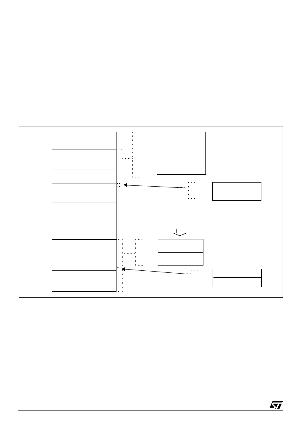
Figure 3. Me m ory Map (ST7 L IT E0)
0000h
007Fh
0080h
00FFh
0100h
0FFFh
1000h
107Fh
1080h
HW Registers
(see Table 2)
RAM
(128 Bytes)
Reserved
Data EEPROM
(128 Bytes)
0080h
00BFh
00C0h
00FFh
The highest address by tes contain the user re set
and interrupt vectors.
The size of Flash Sector 0 is configurable by Option byte.
IMPORTANT: Memory locations marked as “Reserved” must neve r be ac cess ed. A cce ssing a reseved area c an have unpredictable e ffec ts on t he
device.
Short Addressing
RAM (zero page)
64 Bytes Stack
1000h
1001h
see section 7.1 on page 23
RCCR0
RCCR1
F9FFh
FA00h
FFDFh
FFE0h
FFFFh
Reserved
Flash Memory
(1.5K)
Interrupt & Reset Vectors
(see Table 7)
PROGRAM MEMORY
FA00h
FBFFh
FC00h
FFFFh
1.5K FLASH
0.5 Kb yt e s
SECTOR 1
1 Kbyte s
SECTOR 0
FFDEh
RCCR0
FFDFh
RCCR1
see section 7.1 on page 23
8/122
1
REGISTER AND MEMORY MAP (Cont’d)
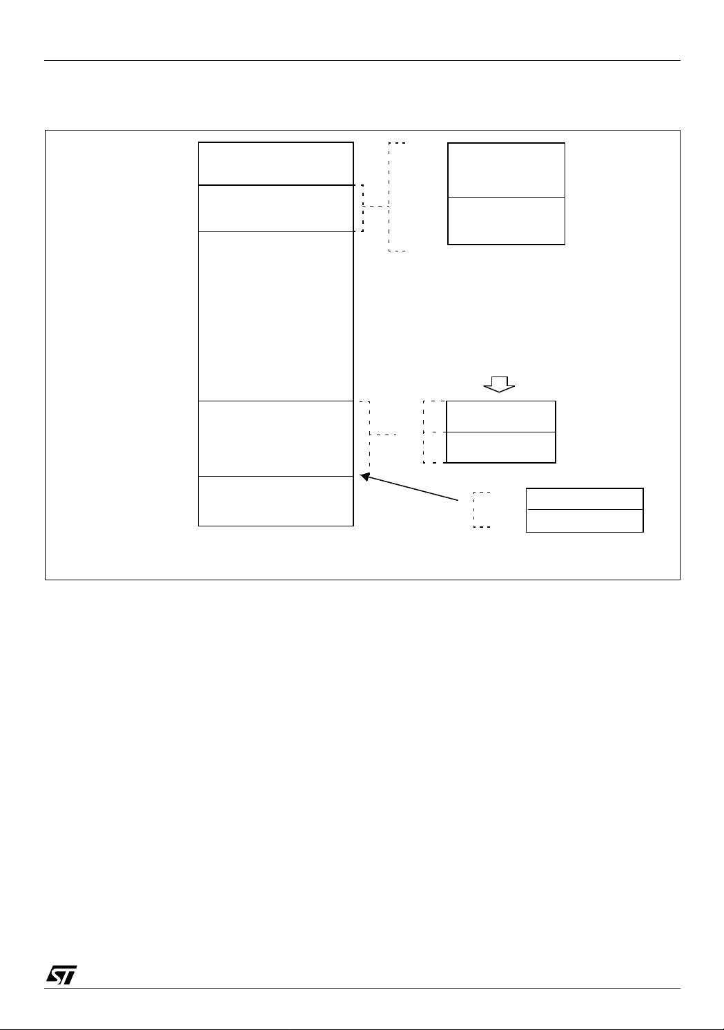
Figure 4. Me m ory Map (ST7SU P E R LI TE )
ST7LITE0, ST7SUPERLITE
0000h
007Fh
0080h
00FFh
0100h
FBFFh
FC00h
FFDFh
FFE0h
FFFFh
HW Registers
(see Table 2)
RAM
(128 Bytes)
Reserved
Flash Memory
(1K)
Interrupt & Reset Vectors
(see Table 7)
FC00h
FDFFh
FE00h
FFFFh
0080h
00BFh
00C0h
00FFh
Short Addressing
RAM (zero page)
64 Bytes S tack
1K FLASH
PROGRAM MEMORY
0.5 Kbytes
SECTOR 1
0.5 Kbytes
SECTOR 0
FFDEh
FFDFh
see section 7.1 on page 23
RCCR0
RCCR1
9/122
1
ST7LITE0, ST7SU PERLITE
REGISTER AND MEMORY MAP (Cont’d)
Legend: x=unde fined, R/W=rea d/write
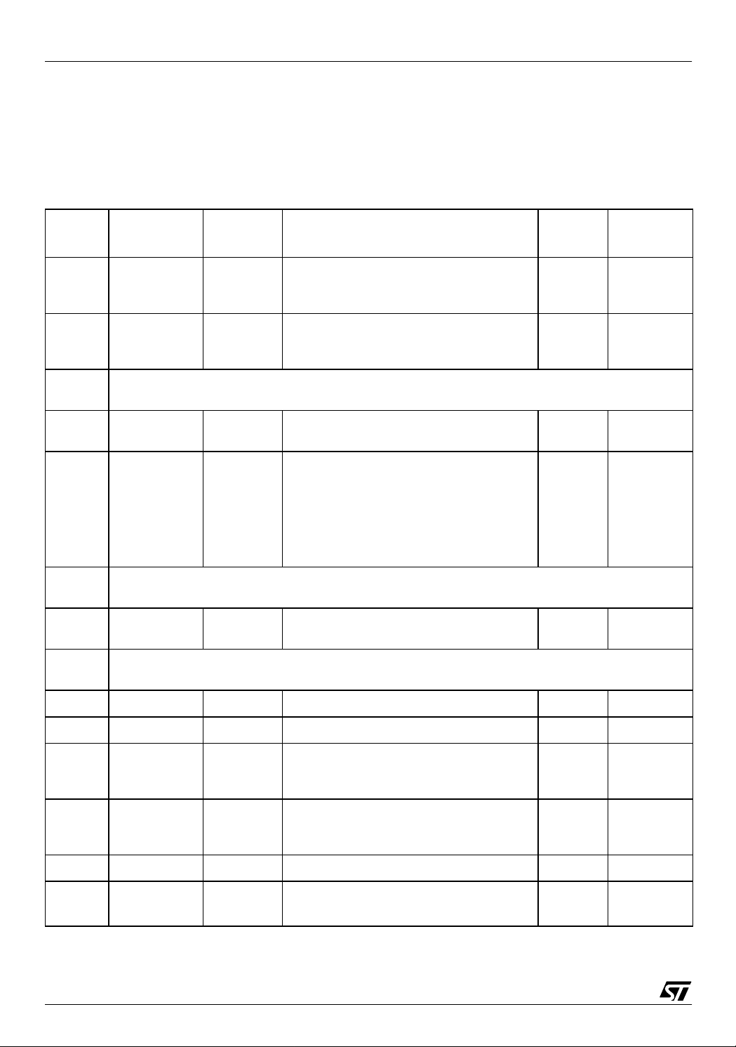
Table 2. Hardware Register Map
Address Block
0000h
0001h
0002h
0003h
0004h
0005h
0006h to
000Ah
000Bh
000Ch
000Dh
000Eh
000Fh
0010h
0011h
0012h
0013h
0014h to
0016h
0017h
0018h
Port A
Port B
LITE
TIMER
AUTO-RELOAD
TIMER
AUTO-RELOAD
TIMER
Register
Label
PADR
PADDR
PAOR
PBDR
PBDDR
PBOR
LTCSR
LTICR
ATCSR
CNTRH
CNTRL
ATRH
ATRL
PWMCR
PWM0CSR
DCR0H
DCR0L
Register Name
Port A Data Register
Port A Data Direction Register
Port A Option Register
Port B Data Register
Port B Data Direction Register
Port B Option Register
Reserved area (5 bytes)
Lite Timer Control/Status Register
Lite Timer Input Capture Register
Timer Control/Sta tus Registe r
Counter Register High
Counter Register Low
Auto-Reload Register High
Auto-Reload Register Low
PWM Output Control Register
PWM 0 Control/Status Register
Reserved area (3 bytes)
PWM 0 Duty Cycle Register High
PWM 0 Duty Cycle Register Low
Reset
Status
1)
00h
00h
40h
1)
E0h
00h
00h
xxh
xxh
00h
00h
00h
00h
00h
00h
00h
00h
00h
Remarks
R/W
R/W
R/W
R/W
R/W
2)
R/W
R/W
Read Only
R/W
Read Only
Read Only
R/W
R/W
R/W
R/W
R/W
R/W
0019h to
002Eh
0002Fh FLASH FCSR Flash Control/Sta tus Registe r 00h R/W
00030h EEPROM EECSR Data EEPROM Control/Status Register 00h R/W
0031h
0032h
0033h
0034h
0035h
0036h
0037h ITC EICR External Interrupt Control Register 00h R/W
0038h
0039h
10/122
SPI
ADC
CLOCKS
SPIDR
SPICR
SPICSR
ADCCSR
ADCDAT
ADCAMP
MCCSR
RCCR
SPI Data I/O Register
SPI Control Register
SPI Control/Status Register
A/D Control Status Register
A/D Data Register
A/D Amplifier Control Register
Main Clock Control/Status Register
RC oscillator Control Register
Reserved area (22 bytes)
xxh
0xh
00h
00h
00h
00h
00h
FFh
1
R/W
R/W
R/W
R/W
Read Only
R/W
R/W
R/W

ST7LITE0, ST7SUPERLITE
Address Block
003Ah SI SICSR System Integrity Control/Status Register 0xh R/W
003Bh to
007Fh
Register
Label
Register Name
Reserved area (45 bytes)
Reset
Status
Remarks
Notes:
1. The contents of the I/O p ort DR registers are readable only i n out put conf iguration. I n i nput conf iguration, the values of the I/O pins are returned instead of the DR register contents.
2. The bits associated with unavailable pins must always keep their reset value.
11/122
1

ST7LITE0, ST7SU PERLITE
4 FLASH PROGRAM MEMORY
4.1 In troduction
The ST7 single voltage extended Flash (XFlash) is
a non-volatile memory that can be electrically
erased and programmed either on a by te-by-byte
basis or up to 32 bytes in parallel.
The XFlash devices can be programmed off-board
(plugged in a programming tool) or on-board using
In-Circuit Programming or In-Application Programming.
The array matrix organ isation allows each sector
to be erased and reprogrammed wi thout affecting
other sectors.
4.2 Main Features
■ ICP (In-Circuit Programming)
■ IAP (In-Application Programming)
■ ICT (In-Circuit Testing) for downloading and
executing user application test patterns in RAM
■ Sector 0 size configurable by option byte
■ Read-out and write protection against piracy
4.3 PROGRAMMING MODES
The ST7 can be programmed in three different
ways:
– Insertion in a programming tool. In this mode,
FLASH sectors 0 and 1, option byte row and
data EEPROM can be programmed or
erased.
– In-Circuit Programming. In this mode, FLAS H
sectors 0 and 1, option byte row and data
EEPROM can be programmed or erased without removing the device from the application
board.
– In-Application Programming. In this mode,
sector 1 and data EEPROM can be programmed or erased without removing the device from the appli cation board a nd while the
application is running.
4.3.1 In-Circuit Programming (ICP)
ICP us es a pr ot o c ol c al l e d I CC ( I n- Ci r c ui t C om mu nication) which allows an ST7 plugged on a printed circuit board (PCB) to communicate with an external programming device connected via cable.
ICP is performed in three steps:
Switch the ST7 to ICC mode (In-Circuit Communications). This is done by driving a specific signal
sequence on the ICCCLK/DATA pins while the
RESET pin is pulled low. When the ST7 enters
ICC mode, it fetches a specific RESET vector
which points to the ST7 System Memory containing the ICC protocol routine. This routine enables
the ST7 to receive bytes from the ICC interface.
– Download ICP Driver cod e in RAM from the
ICCDATA pin
– Execute ICP Driver code in RAM to program
the FLASH memory
Depending on the ICP Driver code downloaded in
RAM, FLASH memo ry programming can be fully
customized (number of bytes to program, program
locations, or selection of the serial communication
interface for downloading).
4.3.2 In Application Programming (IAP)
This mode uses an IAP Driver program previously
programmed in Sector 0 by the user (in ICP
mode).
This mode is fully controlled by user software. This
allows it to be adapted to the user application, (user-defined strategy for entering programming
mode, choice of c om mun ications protoc ol used t o
fetch the data to be stored etc.)
IAP mode can be used to program any memory areas except Sector 0, which is write/erase protected to allow recovery in case errors occur during
the programming operation.
12/122
1
FLASH PROGRAM MEMORY (Cont’d)
ST7LITE0, ST7SUPERLITE
4.4 ICC interface
ICP needs a minimum of 4 and u p to 6 pins to be
connected to the programming tool. These pins
are:
– RESET
–V
: device reset
: device power supply ground
SS
– ICCCLK: ICC output serial clock pin
– ICCDATA: ICC input serial data pin
– CLKIN: main clock input for external source
: application board power supply (option-
–V
DD
al, see Note 3)
Notes:
1. If the ICCCLK or ICCDATA pins are only use d
as outputs in the application, no signal i so lation is
necessary. As soon as the Programming Tool is
plugged to the board, even if an ICC session is not
in progress, the ICCCLK and ICCDATA pins are
not available for the application. If they are used as
inputs by the application, isolation such as a serial
resistor has to be implemented in case another device forces the signal. Refer to the Programming
Tool documentation for recommended resistor values.
2. During the ICP session, the programming tool
must control the RESET pin. This can lead to conflicts between the programming tool and the appli-
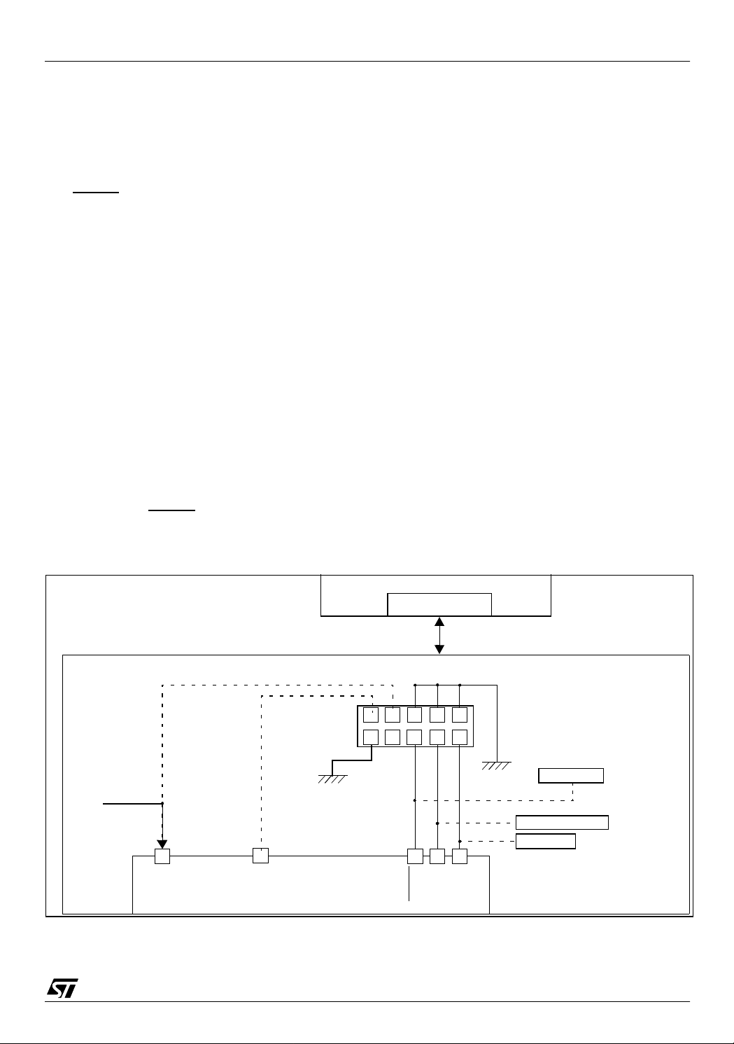
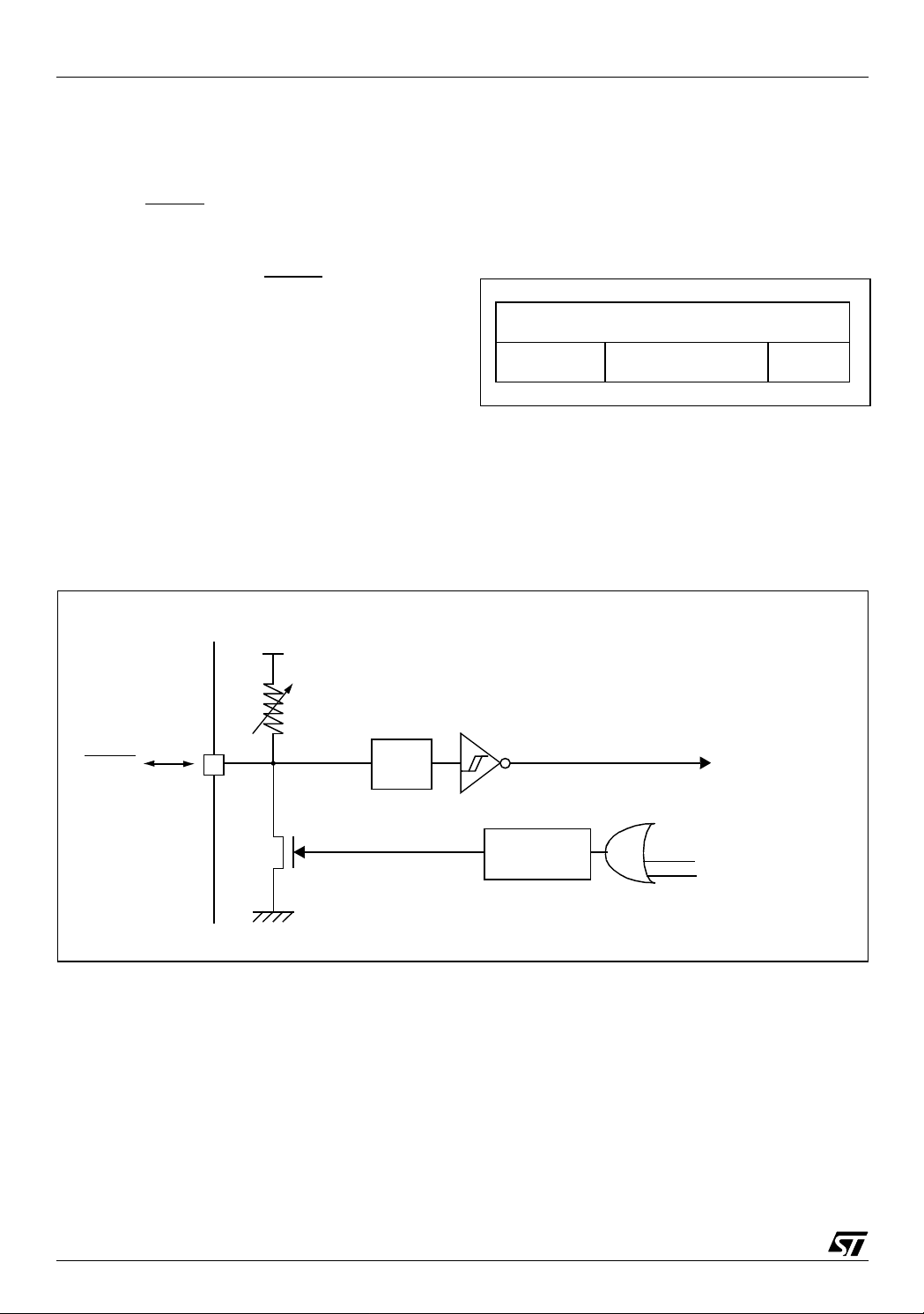
Figure 5. Typical ICC Interface
cation reset circuit if it drives more than 5mA at
high level (push pull output or pull-up resistor<1K).
A schottky diode can be u sed to isolate t he application RESET circuit in this case. When using a
classical RC network with R>1K or a reset management IC with open drain outpu t and pull-up resistor>1K, no additional com ponents are needed.
In all cases the user must ensure that no external
reset is generated by the application during the
ICC session.
3. The use of Pin 7 of the ICC connec tor depends
on the Programming Tool architecture. This pin
must be connected when using most ST Programming Tools (it is used to monitor the application
power supply). Please refer to the Programming
Tool manual.
4. Pin 9 has to be connected t o the CLKIN pin of
the ST7 when the clock is not avai lable in the application or if the selected clock option is not programmed in the option byte.
5. During reset, this pin must be held at high level
to avoid entering ICC mode unexpectedly (this is
guaranteed by the internal pull-up if the application
leaves the pin floating).
APPLICATION
POWER SUPPLY
OPTIONAL
(See Note 3)
VDD
OPTIONAL
(See Note 4)
CLKIN
ST7
PROGRAMMING TOOL
ICC CONNECTOR
ICC Ca ble
ICC CONNECTOR
HE10 CONNECTORTYPE
975 3
1
246810
RESET
ICCCLK
ICCDATA
APPL ICATION BOARD
APPLICATION
RESET SOURCE
See Note 2
See Notes 1 and 5
See Note 1
APPLICATION
I/O
13/122
1
ST7LITE0, ST7SU PERLITE
FLASH PROGRAM MEMORY (Cont’d)
4.5 Memory Protection
There are two different types of memory protection: Read Out Protection and Write/Erase Protection which can be applied individually.
4.5.1 Read out Protection
Read out protection, when selected, makes it impossible to extract the m emory content from the
microcontroller, thus preventing piracy. Both program and data E
2
memory are protected.
In flash devices, this protection is removed by reprogramming the option. In this case, both program and data E
2
memory are automatically
erased, and the device can be reprogrammed.
Read-out protection selection depends on the de-
vice type:
– In Flash devices it is enabled and removed
through the FMP_R bit in the option byte.
– In ROM devices it is enabled by mask option
specified in the Option List.
4.5.2 Flash Write/Erase Protection
Write/erase protection, when set, makes it impossible to both overwrite and erase program memory. It does not apply to E
2
data. Its purpose is to
provide advanced security to applications and prevent any change bei ng made to the mem ory content.
Warning: Once set, Write/erase protection can
never be removed. A write-protected flash device
is no longer reprogrammable.
Write/erase protection is enabled through the
FMP_W bit in the option byte.
4.6 Related Documentation
For details on Flash program ming and I CC protocol, refer to the ST7 Flash Programming Reference Manual and to th e ST7 ICC Protocol Reference Manual
.
4.7 Register Description FLASH CONTROL/STATUS REGISTER (FCSR)
Read/Write
Reset Value: 000 0000 (00h)
1st RASS Key: 0101 0110 (56h)
2nd RASS Key: 1010 1110 (AEh)
70
00000OPTLATPGM
Note: This register is reserved for programming
using ICP, IAP or other program ming methods. It
controls the XFlash p ro grammin g and erasing operations.
When an EPB or another programming tool is
used (in socket or ICP mode), the RASS k eys are
sent automatically.
Table 3. FLASH Register Map and Reset Values
Address
(Hex.)
002Fh
14/122
Register
Label
FCSR
Reset Value
76543210
00000
1
OPT
0
LAT
0
PGM
0
5 DATA EEPRO M
ST7LITE0, ST7SUPERLITE
5.1 INTRODUCTION
The Electrically Erasable Programmable Read
Only Memory can be us ed as a non volatile back up for storing data. Using the EEPROM requires a
basic access protocol described in this chapter.
Figure 6. EEPR OM Block Dia gram
EECSR
ADDRESS
DECODER
0 E2LAT00 0 0 0 E2PGM
4
DECODE R
ROW
5.2 MAIN FEATURES
■ Up to 32 Bytes programmed in the same cycle
■ EEPROM mono-voltage (charge pump)
■ Chained eras e and programmi n g cycles
■ Interna l c ont ro l of th e g l o bal p rog ra mming cycle
duration
■ WAIT mode management
■ Readout protection against piracy
HIGH VOLTAGE
PUMP
EEPROM
MEMORY MATRIX
(1 ROW = 32 x 8 BITS )
ADDRESS B U S
128128
4
4
DATA
MULTIPLEXER
DATA BUS
32 x 8 BITS
DATA L ATCHES
15/122
1
ST7LITE0, ST7SU PERLITE
DATA EEPROM (Cont’d)
5.3 MEMORY ACCESS
The Data EEPROM memory read/write access
modes are con tr olled by the E2LAT bi t of t he EEPROM Control/Status register (EECSR). The flowchart in Figure 7 describes these different memory
access modes.
Read Operation (E2LAT=0)
The EEPROM can be read as a normal ROM location when the E2LAT bit of t he EECSR register is
cleared. In a read cycle, the byte to be accessed is
put on the dat a bus in l ess th an 1 CPU clock cycle .
This means that reading data from EEPROM
takes the same time as reading data from
EPROM, but this memory cannot be used to execute machine code.
Write Operation (E2LAT=1)
To access the write mode, the E2LAT bit has to be
set by software (the E2PGM bit remains cleared).
When a write access to the EEPROM area occurs,
Figure 7. Data EE P R OM Pr ogramming Fl owchart
READ MODE
E2LAT=0
E2PGM=0
the value is l atched in side the 32 data lat ches according to its address.
When PGM bit is set by the software, all the previous bytes written in the data latches (up to 32) are
programmed in the EEPR OM cells. The effective
high address (row) is determined by the la st EEPROM write sequence. To avoid wrong programming, the user must take care that all the bytes
written between two programming sequences
have the same high address: only the five Least
Significant Bits of the address can change.
At the end of the programming cycle, the PGM and
LAT bits are cleared simultaneously.
Note: Care should be taken during the programming cycle. Writing to the same memory location
will over-program the memory (logical AND between the two w rite access data result) because
the data latches are only cleared at the end of the
programming cycle and by the falling e dge of the
E2LAT bit.
It is not possible to read the latched data.
This note is ilustrated by the Figure 9.
WRITE MODE
E2LAT=1
E2PGM= 0
16/122
1
READ BYTES
IN EEPROM AREA
CLEARED BY HA R D WARE
WRITEUPTO32BYTES
(with the same 11 MSB of the address)
IN EEPROM AREA
START PROGRAMMING CY CL E
E2PGM=1 (set by software)
E2LAT=1
01
E2LAT
DATA EEPROM (Cont’d)
2
Figure 8. Data E
PROM Write Operation
ST7LITE0, ST7SUPERLITE
DEFINITION
E2LAT bit
E2PGM bit
Row / Byte
⇓
ROW
Byte 1 Byte 2 Byte 32
Set by USER application
0
1
...
N
PHASE 1
Writing data latches Waiting E2PGM and E2LAT to fall
0 1 2 3 ... 30 31 Physical Address
⇒
Nx20h...Nx20h+1Fh
Read operation impossible
Programming cycle
PHASE 2
00h...1Fh
20h...3Fh
Read operation possible
Cleared by hardware
Note: If a programming cycle is interrupted (by software or a reset action), the integrity of the data in mem-
ory is not guaranteed.
17/122
1
ST7LITE0, ST7SU PERLITE
DATA EEPROM (Cont’d)
5.4 POWER SAVI NG MO DE S Wait mode
The DATA EEPROM can enter WAIT mode on execution of the WFI inst ruction of the m icrocontroller or when the microcontroller enters Active-HALT
mode.The DATA EEPROM will immediately enter
this mode if there is no programming i n progress,
otherwise the DATA EEPROM will finish the cycle
and then enter WAIT mode.
Active-Halt mode
Refer to Wait mode.
Halt mode
The DATA EEPROM immediately enters HALT
mode if the microcontroller exec utes the HA LT instruction. Therefore the EEPROM will stop the
function in progress, and data may be corrupted.
5.5 ACCESS ERROR HANDLING
If a read access occurs while E2LAT=1, then the
data bus will not be driven.
If a write access occurs while E2LAT=0, then t he
data on the bu s w ill not be latche d.
If a programming cycl e is interrupted (by software/
RESET action), the memory data will not be guaranteed.
5.6 Data EEPROM Read - ou t Protection
The read-out protection is enabled throug h an option bit (see section 15.1 on page 109).
When this option is selected, the programs and
data stored in the EEPROM memory are protected
against read-out piracy (including a re-write protection). In Flash devices, when this protection is
removed by reprogrammin g the Option Byte, the
entire Pr ogram memeory and EEPR OM is fir st automatically erased.
Note: B oth Progr am Memory and data EEP ROM
are protected using the same option bit.
Figure 9. Data EE P R OM Pr ogramming C ycl e
READ OPERATION NOT POSSIBLE
INTERNAL
PROGRAMMING
VOLTAGE
ERASE CYCLE WRITE CYCLE
WRITEOF
DATA LATCHES
t
PROG
READ OPERATION POSSIBLE
LAT
PGM
18/122
1

ST7LITE0, ST7SUPERLITE
DATA EEPROM (Cont’d)
5.7 REGISTER DESCRIPTION EEPROM CONTROL/STATUS REGISTER (EEC-
SR)
Read/Write
Reset Value: 0000 0000 (00h)
70
000000E2LATE2PGM
Bits 7:2 = Reserved, forced by hardware to 0.
Bit 1 = E2LAT
Latch Access Transfer
This bit is set by software. It is cleared by hardware at the end of the programming cycle. It can
only be cleared by software if the E2PGM bit is
cleared.
0: Read mode
1: Write mode
Bit 0 = E2PGM
Programming control and status
This bit is set by software to begin the programming
cycle. At the end of the programming cycle, this bit
is cleared by hardware.
0: Programming finished or not yet started
1: Programming cycle is in progress
Note: if the E2PGM bit is cleared during the programming cycle, the m emory data is not guaranteed
Table 4. DATA EEPROM Register Map and Reset Values
Address
(Hex.)
0030h
Register
Label
EECSR
Reset Value
76543210
000000
E2LAT0E2PGM
0
19/122
1
ST7LITE0, ST7SU PERLITE
6 CENTRAL PRO CESSING UNIT
6.1 INTRODUCTION
This CPU has a full 8-bit architecture and contains
six internal registers allowing efficient 8-bit data
manipulation.
6.2 MAIN FEATURES
■ 63 basic instructions
■ Fast 8-bit by 8-bit multiply
■ 17 main addressing modes
■ Two 8-bit index registers
■ 16-bit stack pointer
■ Low power mo des
■ Maskable hardware interrupts
■ Non-maskable software interrupt
6.3 CPU REGISTERS
The 6 CPU registers shown in Figure 10 are not
present in the memory mapping and are accessed
by specific instructions.
Figure 10. CPU Registers
70
RESET VALUE = XXh
70
RESET VALUE = XXh
70
RESET VALUE = XXh
Accumulator (A)
The Accumulator is an 8-bit general purpose register used to hold operan ds and the results of the
arithmetic and logic calculations and to manipulate
data.
Index Registers (X and Y)
In indexed addressing modes, these 8-bit registers
are used to create either effective addresses or
temporary storage areas for data manipulation.
(The Cross-Assembler generates a precede instruction (PRE) to indicate that the following instruction refers to the Y register.)
The Y register is not affected by the interrupt automatic procedures (not pushed to and popped from
the stack).
Program Cou nt er (P C )
The program counter is a 16-bit register containing
the address of the next instruction to be executed
by the CPU. It is made of two 8-bit registers PCL
(Program Counter Low which is the LSB) and PCH
(Program Counter High which is the MSB).
ACCUMULATOR
X INDEX REGISTER
Y INDEX REGISTER
15 8
RESET VALUE = RESET VECTOR @ FFFEh-FFFFh
15
RESET VALUE = STACK HIGHER ADDRESS
20/122
PCH
RESET VALUE =
7
70
1C11HI NZ
1X11X1XX
70
8
PCL
1
0
PROGRAM COUNTER
CONDITION CODE REGISTER
STACK POINTER
X = Undefined Value

ST7LITE0, ST7SUPERLITE
CPU REGISTERS (Cont’d)
CONDITION CODE REGISTER (CC)
Read/Write
Reset Value: 111x1xxx
70
111HINZC
The 8-bit Condition Code register c ontains the interrupt mask and four flags represent ative of the
result of the instruction just executed. This register
can also be handled by the PUSH and POP instructions.
These bits can be individually tested and/or controlled by specific instructions.
Bit 4 = H
Half carry
.
This bit is set by hardware when a carry occurs between bits 3 and 4 of t he ALU during an ADD or
ADC instruction. It is reset by hardware during the
same instructions.
0: No half carry has occurred.
1: A half carry has occurred.
This bit is tested using the JRH or JRNH instruction. The H bit is useful in BCD arithmetic subroutines .
Bit 3 = I
Interrupt mask
.
This bit is set by hardware when entering in interrupt or by software to disable all interrup ts except
the TRAP software interrupt. This bit is cleared by
software.
0: Interrupts are enabled.
1: Interrupts are disabled.
This bit is controlled by the RIM, SIM and IRET instructions and is tested by the JRM and JRNM instructions.
Note: Interrupts requested while I is set are
latched and can be processed whe n I is cleared.
By default an interrupt routine is not in terruptable
because the I bi t is set by hardware at the start of
the routine and reset by the IRET instruction at the
end of the routine. If the I bit is cleared by software
in the interrupt routine, pending interrupts are
serviced regardless of the priority level of the current interrupt routine.
Bit 2 = N
Negative
.
This bit is set and cleared by hardware. It is representative of the result sign of the last arithmeti c,
logical or data manipulation. It is a copy of the 7
bit of the result.
0: The result of the last operation is positive or null.
1: The result of the last operation is negative
(i.e. the most significant bit is a logic 1).
This bit is accessed by the JRMI and JRPL instructions.
Zero
Bit 1 = Z
.
This bit is set and cleared by hardware. This bit indicates that the result of the last arithmetic, logical
or data manipulation is zero.
0: The result of the last operation is different from
zero.
1: The result of the last operation is zero.
This bit is accessed by the JREQ and JRNE test
instructions.
Bit 0 = C
Carry/borrow.
This bit is set and cleared b y hardware and software. It indicates an overflow or an underflow has
occurred during the last arithmetic operation.
0: No overflow or underflow has occurred.
1: An overflow or underflow has occurred.
This bit is driven by the SCF and RCF instructions
and tested by the JRC and JRNC instructions. It is
also affected by the “bit test and branch”, shift and
rotate instructions.
th
21/122
1
ST7LITE0, ST7SU PERLITE
CPU REGISTERS (Cont’d)
Stack Pointer (SP)
Read/Write
Reset Value: 00 FFh
15 8
00000000
70
1 1 SP5 SP4 SP3 SP2 SP1 SP0
The Stack Pointer is a 16-bit register which is always pointing to the next free location in the stack.
It is then decremented after data has been pushed
onto the stack and incremented before data is
popped from the stack (see Figure 11).
Since the stack is 64 bytes deep, the 10 most significant bits are forced by hardw are. Following a n
MCU Reset, or after a Reset Stack Pointe r instruction (RSP), the Stack Pointer contains its reset value (the SP5 to SP0 bits are set) which is the stack
higher address.
The least significant byte of the Stack Pointer
(called S) can be directly accessed by a LD instruction.
Note: When the lower limit is exceeded, the Stack
Pointer wraps around to the stack upper limit, wi thout indicating the s tack overflow. The previously
stored information is then o verwritten and therefore lost. The stack also wraps in case of an underflow.
The stack is used to save the retu rn address during a subroutine call and the CPU context during
an interrupt. The user may also directly manipulate
the stack by means of the PUSH and POP instructions. In the case of an interrupt, the PCL is stored
at the first location point ed to by the SP. Then the
other registers are stored in the next locations as
shown in Figure 11.
– When an interrupt is received, the SP is decre-
mented and the context is pushed on the stack.
– On return from interrupt, the SP is incremented
and the context is popped from the stack.
A subroutine call occupies two locations and an interrupt five locat ions i n the sta ck ar ea.
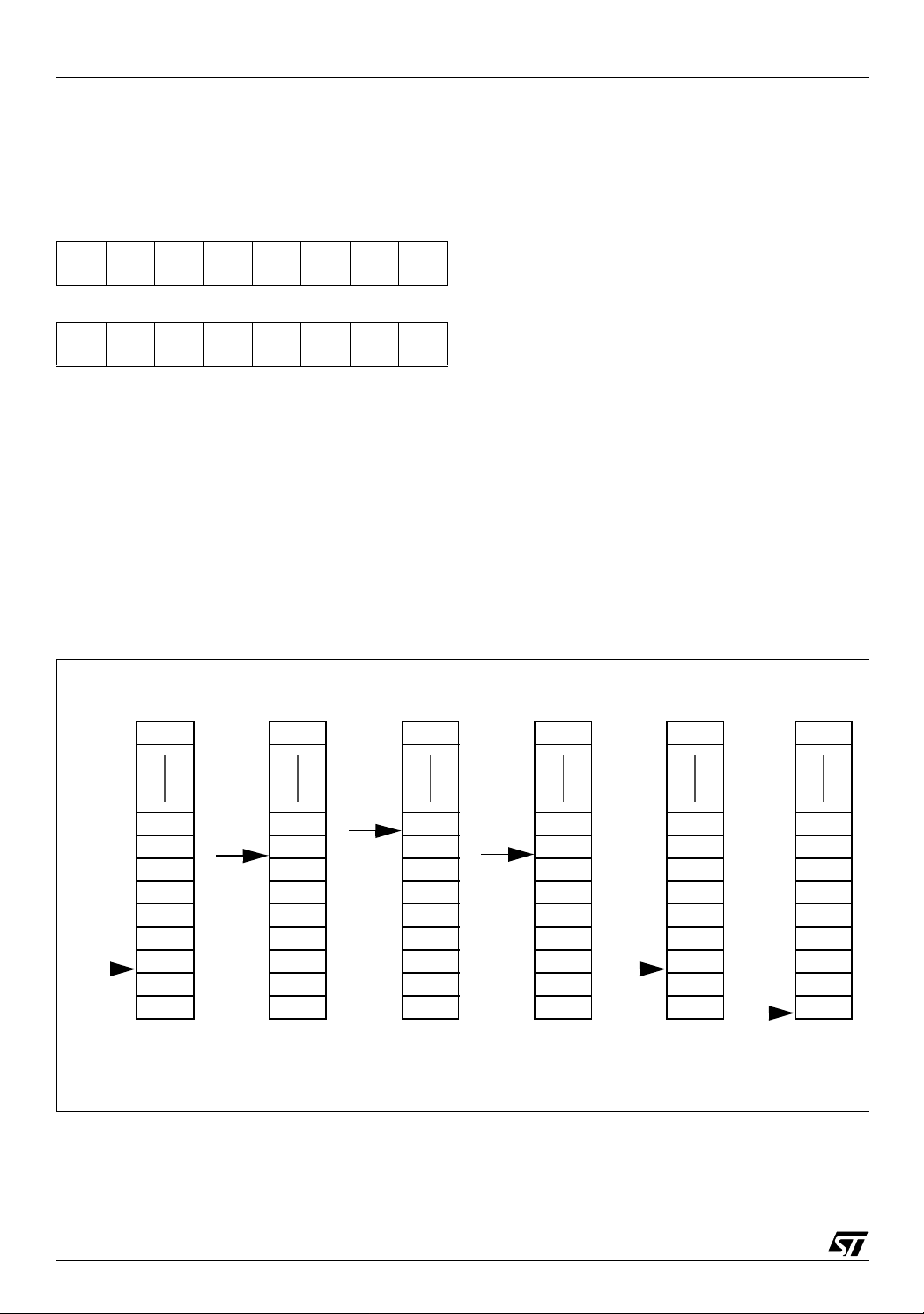
Figure 11. Stack Manipulation Example
@ 00C0h
SP
@ 00FFh
CALL
Subroutine
SP
PCH
PCL
Stack Higher Address = 00FFh
Stack Lower Address =
Interrupt
event
SP
CC
A
X
PCH
PCL
PCH
PCL
00C0h
PUSH Y POP Y IRET
SP
Y
CC
A
X
PCH
PCL
PCH
PCL
CC
A
X
PCH
PCL
PCH
PCL
SP
PCH
PCL
RET
or RSP
SP
22/122
1

7 SUPPLY, RESET AND CLOCK MANA GEMENT
ST7LITE0, ST7SUPERLITE
The device includes a range of utility features for
securing the application in critical situations (for
example in case of a power brown-out), and reducing the number of external components.
Main features
■ Clock Management
– 1 MHz internal RC oscillator (enabled by op-
tion byte)
– External Clock Input (enabled by option byte)
– PLL for multiplying the frequency by 4 or 8
(enabled by option byte)
■ Reset Sequence Manager (RSM)
■ System Integrity Management (SI)
– Main supply Low voltage detection (LVD) with
reset generation (enabled by option byte)
– Auxiliary Voltage detector (AVD) with interrupt
capability for monitoring the main supply (en-
abled by option byte)
7.1 INTERNAL RC OSCILLATOR ADJUSTMENT
The ST7LITE0 and ST7SUPERLITE contain an internal RC oscillator with an accuracy of 1% for a
given device, temperat ure and voltage. It must be
calibrated to obtain the frequenc y required in the
application. This is done by software writing a calibration value in the RCCR (RC Control Register).
Whenever the microcontroller is reset, the RCCR
returns to its default value (F F h), i.e. each time the
device is reset, the calibration value must be loaded in the RCCR. Predefined calibration values are
stored in EEPROM for 3.0 and 5V V
ages at 25°C, as shown in the following table.
supply volt-
DD
Notes:
– See “ELECTRICAL CHARACTERISTICS” on
page 78. for more information on the frequency
and accuracy of the RC oscillator.
– To improve clock stability, it is recommended to
place a decoupling capacitor between the V
DD
ST7FLITE02 /
ST7FLITE05 /
ST7FLITES2 /
ST7FLITES5
Address
FFDEh
FFDFh
RCCR C onditions
V
=5V
RCCR0
RCCR1
and V
DD
T
=25°C
A
f
=1MHz
RC
V
=3.0V
DD
T
=25°C
A
f
=700KHz
RC
pins as close as possible to the ST7 de-
SS
ST7FLITE09
Address
1000h and
FFDEh
1001h andFFDFh
vice.
– These two bytes ar e syste matically pr ogrammed
by ST, including on FASTROM devices. Consequently, customers intending to use FASTROM
service must not use these two bytes.
Caution: If the voltage or temperature conditions
change in the application, the frequency may need
to be recalibrated.
Refer to application note AN1 324 for information
on how to calibrate the RC frequency using an external reference signal.
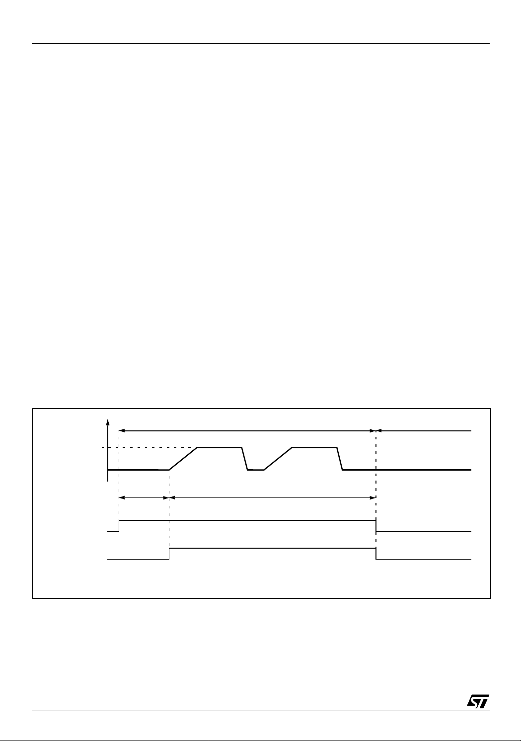
7.2 PHASE LOCKED LOOP
The PLL can be used to multiply a 1MHz f requency from the RC oscillator or the external clock by 4
or 8 to obtain f
of 4 or 8 MHz. The PLL is ena-
OSC
bled and the multiplication factor of 4 or 8 is selected by 2 option bits.
– The x4 PLL is intended for operation with V
DD
in
the 2.4V to 3.3V range
– The x8 PLL is intended for operation with V
the 3.3V to 5.5V range
DD
in
Refer to Section 15.1 for the option byte descrip-
tion.
If the PLL is disabled and the RC oscillator is enabled, then f
OSC =
1MHz.
If both the RC oscillator and the PLL are disabled,
is driven by the external clock.
f
OSC
23/122
1
ST7LITE0, ST7SU PERLITE
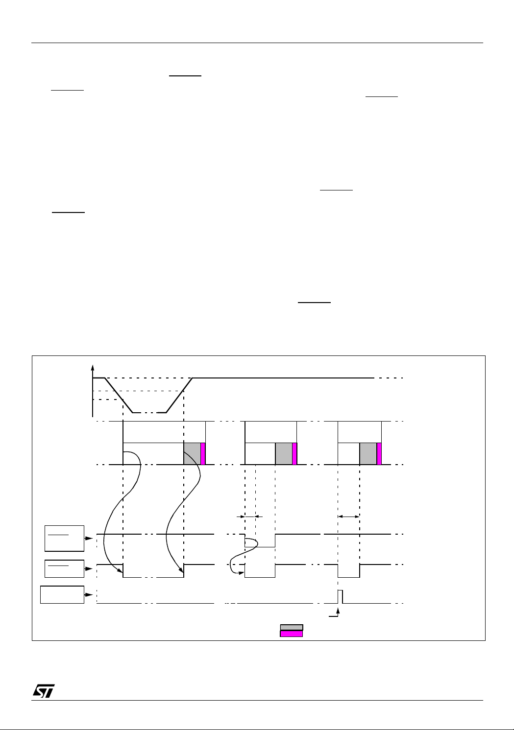
Figure 12. PLL Output Frequency Timing
Diagram
LOCKED bit set
4/8 x
input
freq.
t
STAB
t
LOCK
t
STARTUP
Output freq.
t
When the PLL is started, after reset or wakeup
from Halt mode or AWUFH mode , it outputs the
clock after a delay of t
STARTUP
.
When the PLL output signal reaches the operating
Bit 1 = MCO
This bit is read/write by software and cleared by
hardware after a reset. This bit allows to ena ble
the MCO output clock.
0: MCO clock disabled, I/O port free for general
purpose I/O.
1: MCO clock enabled.
Bit 0 = SMS
This bit is read/write by software and cleared by
hardware after a reset. This bit selects the input
clock f
0: Normal mode (f
1: Slow mode (f
RC CONTROL REGISTER (RCCR)
Read / Write
Reset Value: 1111 1111 (FFh)
70
Main Clock Out enable
Slow Mode select
OSC
or f
/32.
OSC
CPU = fOSC
CPU = fOSC
/32)
frequency, the LOCKED bit in the SICSCR register
is set. Full PLL accur acy (ACC
a stabilization time of t
STAB
) is reached after
PLL
(see Figure 12 and
CR70 CR60 CR50 CR40 C R30 CR20 CR10
13.3.4 Internal RC Oscillator and PLL)
Refe r to section 7.5.4 on page 32 for a description
of the LOCKED bit in the SICSR register.
Bits 7:0 = CR[7:0]
justment Bits
These bits must be written immediately after reset
RC Oscillator Frequency Ad-
to adjust the RC oscillator frequency and to obtain
7.3 REGISTER DESCRIPTION MAIN CLOCK CONTROL/STATUS REGISTER
(MCCSR)
Read / Write
Reset Value: 0000 0000 (00h)
an accuracy of 1%. The application ca n store the
correct value for each voltage range in EEPROM
and write it to this register at start-up.
00h = maximum available frequency
FFh = lowest available frequency
Note: To tune the oscillator, write a series of differ-
70
ent values in the register until the correct frequency is reached. The fastest met hod is to use a di-
0000000
MCO SMS
chotomy starting with 80h.
CR
0
Bits 7:2 = Reserved, must be kept cleared.
Table 5. Clock Register Map and Reset Values
Address
(Hex.)
0038h
0039h
24/122
Register
Label
MCCSR
Reset Value
RCCR
Reset Value
76543210
000000
CR70
1
CR60
1
CR50
1
MCO
0
CR40
1
1
CR30
1
CR20
1
CR10
1
SMS
0
CR0
1
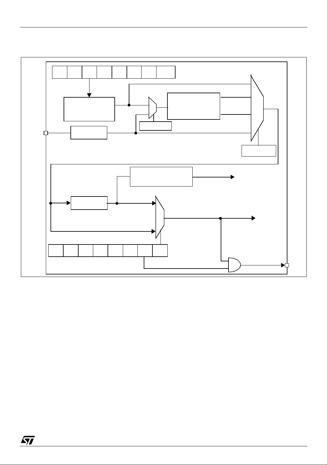
Figure 13. Clock Management Block Diagram
CR4CR7 CR0CR1CR2CR3CR6 CR5 RCCR
Tunable
Oscillator1% RC
PLL 1MHz -> 8MHz
PLL 1MHz -> 4MHz
ST7LITE0, ST7SUPERLITE
1MHz
8MHz
f
4MHz
OSC
CLKIN
f
OSC
7
/2 DIVIDER
/32 DIVIDER
Option byte
8-BIT
LITE TIMER COUNTER
f
/32
f
OSC
OSC
1
0
SMSMCO
0
MCCSR
0 to 8 MHz
Option byte
f
LTIMER
(1ms timebase @ 8 MHz f
f
CPU
TO CPU AND
PERIPHERALS
(except LITE
TIMER)
OSC
f
CPU
)
MCO
25/122
1
ST7LITE0, ST7SU PERLITE
7.4 RESET SEQUENCE MANAGER (RSM)
7.4.1 Introd uct i on
The reset sequence manager in cludes three RESET sources as shown in F igure 15:
■ External RESET source pulse
■ Internal LVD RESET (Low Voltage Detection)
■ Internal WATCHDOG RESET
These sources act on the RESET
pin and it is al-
ways kept low during the delay phase.
The RESET service routine vector is fixed at ad-
dresses FFFEh-FFFFh in the ST7 memory map.
The basic RESET s eque nc e cons i sts o f 3 p has es
as shown in Figure 14:
■ Active Phase depending on the RESET source
■ 256 CPU clock cycle delay
■ RESET vector fetch
The 256 CPU clock cycle delay allows the oscillator to stabilise and ensures that recovery has taken place from the Reset state.
Figure 15. Reset Block Diagram
V
DD
The RESET vector fetch phase duration is 2 clock
cycles.
If the PLL is enabled by opt ion byte, it outputs the
clock after an additional delay of t
STARTUP
(see
Figure 12).
Figure 14. RESET Sequence Phases
RESET
Active Phase
INTERNAL RESET
256 CLOCK CYCLES
FETCH
VECTOR
RESET
R
ON
FILTER
PULSE
GENERATOR
INTERNAL
RESET
WATCHDO G RESET
LVD RESET
26/122
1
RESET SEQUENCE MANAGER (Cont’d)
ST7LITE0, ST7SUPERLITE
7.4.2 Asynchronous External RES ET
The RESET
output with integrated R
pin is both an input and an open-drain
weak pull-up resistor.
ON
pin
This pull-up has no fixe d value but varies in accordance with the input voltage. It
can be pulled
low by external circuitry to reset the device. See
Electrical Characteristic section for more details.
A RESET signal originating from an external
source must have a duration of at least t
h(RSTL)in
in
order to be recognized (see Figure 16). This de-
tection is asynchronous and therefore the MCU
can enter reset state even in HALT mode.
The RESET
pin is an asynchronous signal which
plays a major role in EMS performance. In a noisy
environment, it is recommended to follow the
guidelines mentioned in the electr ical characteristics section.
7.4.3 External Power-On RESET
If the LVD is disabled by option byte, to start up t he
microcontroller correctly, the user must ensure by
means of an external reset circuit that the reset
signal is held low until V
level specified for the selected f
is over the m inimum
DD
frequency.
OSC
Figure 16. RESET Sequences
V
DD
A proper reset signal for a slow rising V
supply
DD
can generally be provided b y an e xternal RC ne twork connected to the RESET
pin.
7.4.4 Internal Low Voltage Detector (LVD)
RESET
Two differen t RESET sequences caused by the internal LVD circuitry can be distinguished:
■ Power-On RESET
■ Voltage Drop RESET
The device RESET
pulled low when V
V
DD<VIT-
(falling edge) as shown in Fi gure 16.
The LVD filters spikes on V
pin acts as an output that is
DD<VIT+
(rising edge) or
larger than t
DD
g(VDD)
to
avoid parasitic resets.
7.4.5 Internal Watchdog RESET
The RESET sequence generated by a internal
Watchdog counter overflow is shown in Figure 16.
Starting from the Watchdog counter underflow, the
device RESET
low during at least t
pin acts as an output that is pulled
w(RSTL)out
.
V
IT+(LVD)
V
IT-(LVD)
EXTERNAL
RESET
SOURCE
RESET PIN
WATCHDOG
RESET
RUN
LVD
RESET
ACTIVE PHASE
RUN
t
h(RSTL)in
EXTERNAL
RESET
ACTIVE
PHASE
WATCHDOG UNDERFLOW
RUN RUN
INTERNAL RESET (256 T
VECTOR FETCH
WATCHDO G
RESET
ACTIVE
PHASE
t
w(RSTL)out
CPU
)
27/122
1
ST7LITE0, ST7SU PERLITE
7.5 SYSTEM INTEGRITY MANAGEMENT (SI)
The System Integrity Managem ent block contains
the Low voltage Detector (LVD) and Auxiliary Voltage Detector (AVD) functions. It is managed by
the SICSR register.
7.5.1 Low Voltage Detector (LVD)
The Low Voltage Detector funct ion (LVD) generates a static reset when the V
below a V
IT-(LVD)
reference value. This means that
it secures the power-up as well as the power-down
keeping the ST7 in reset.
The V
IT-(LVD)
lower than the V
reference value for a voltage drop is
IT+(LVD)
reference value for poweron in order to avoid a parasitic reset when the
MCU starts running and sinks current on the supply (hysteresis).
The LVD Reset circuitry generates a reset when
is below:
V
DD
–V
–V
IT+(LVD)
IT-(LVD)
when VDD is rising
when VDD is falling
The LVD func t ion is illustrated in F igure 17.
The voltage threshold can be configured by option
byte to be low, m edium or high. S ee section 15.1
on page 109.
supply voltage is
DD
Provided the minimum V
the oscillator frequency) is above V
value (guaranteed for
DD
IT-(LVD)
, the
MCU can only be in two modes:
– under full software control
– in static safe reset
In these conditions, secure operation is always ensured for the application without the need for external reset hardware.
During a Low Voltage Detector Reset, the RESET
pin is held low, thus p ermitting the MCU to reset
other devices.
Notes:
The LVD is an optional function whi ch can be se-
lected by option byte. See section 15.1 o n page
109.
It allows the device to be used without any external
RESET circuitry.
If the LVD is disabled, an external circuitry must be
used to ensure a proper power-on reset.
Caution: If an LVD reset occurs after a watchdog
reset has oc curred, the LVD will take prio rity and
will clear the watchdog flag.
Figure 17. Low Voltage Detector vs Reset
V
DD
V
IT+
(LVD)
V
IT-
(LVD)
RESET
V
hys
28/122
1
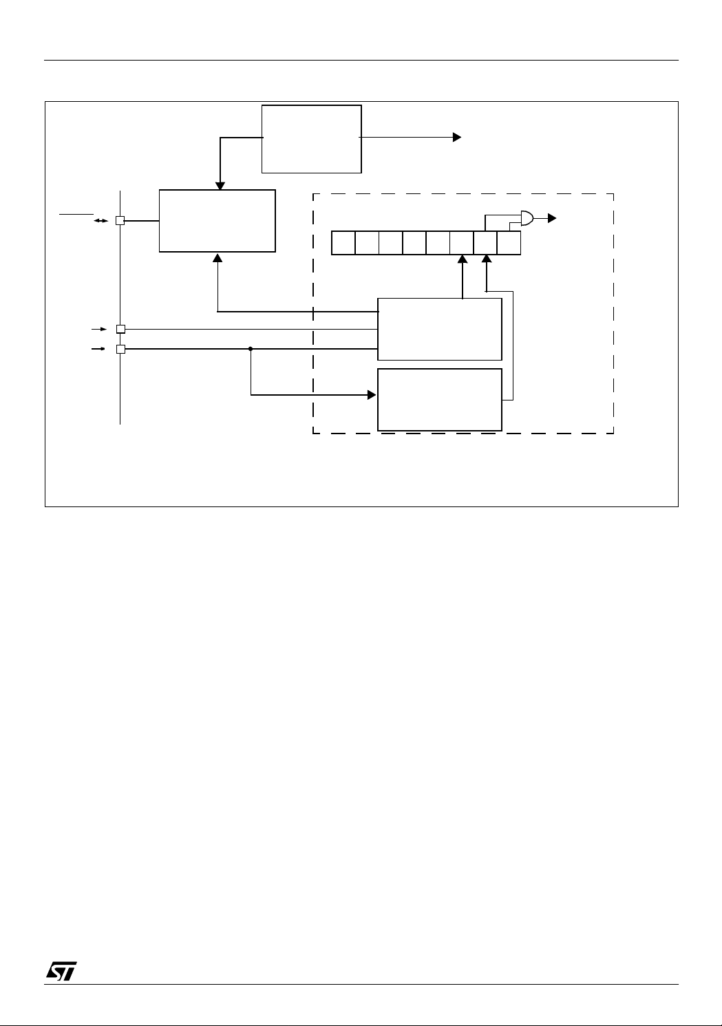
Figure 18. Reset and Supply Management Block Diagram
ST7LITE0, ST7SUPERLITE
RESET
V
SS
V
DD
RESET SEQUENCE
MANAGER
(RSM)
WATCHDOG
TIMER (WDG)
STATUS FLAG
SYSTEM INTEGRITYMANAGEMENT
SICSR
LOC
00
0
7
0
LOW VOLTAGE
DETEC TOR
AUXILIARY VOLTAGE
DETEC TOR
KED
(LVD)
(AVD)
RF IE
AVD Interrupt Request
AVDAVDLVD
F
0
29/122
1
ST7LITE0, ST7SU PERLITE
SYSTEM INTEGRITY MANAGEMENT (Cont’d)
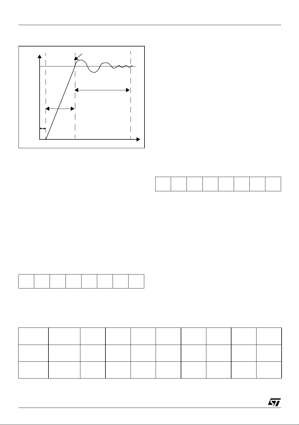
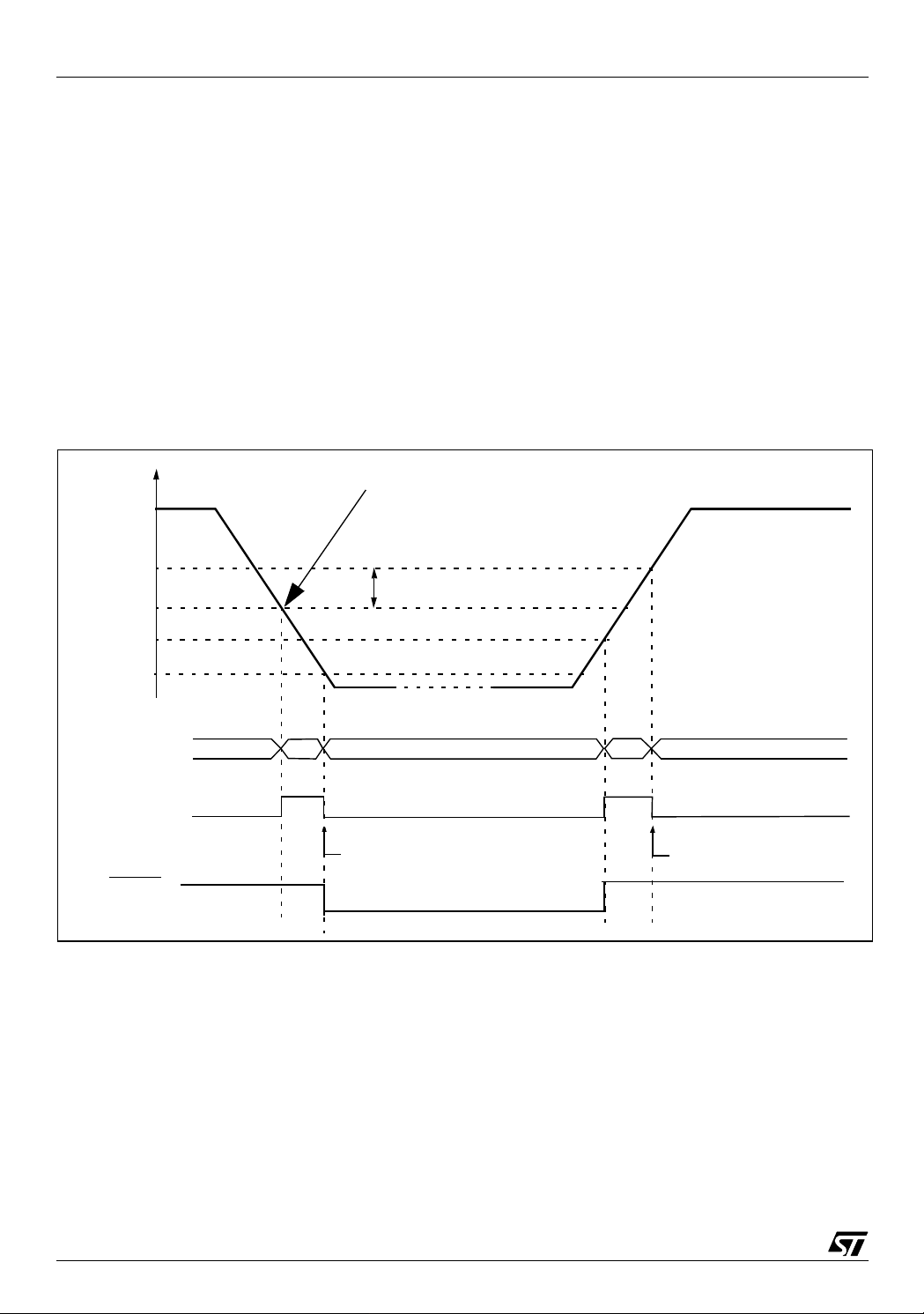
7.5.2 Auxiliary Voltage Detector (AVD)
The Voltage Detector function (AVD) is based on
an analog comparison between a V
V
IT+(AVD)
ply voltage (V
for falling voltage is lower than the V
reference value and the VDD main sup-
). The V
AVD
IT-(AVD)
IT-(AVD)
reference value
IT+(AVD)
ence value for rising voltage in order to avoid parasitic detection (hysteresis).
The output of the AVD comparator is directly readable by the application software through a real
time status bit (AVDF) in the S I CSR regi ster. Th is
bit is read only.
Caution: The AVD functions only if the LVD is enabled through the option byte.
and
refer-
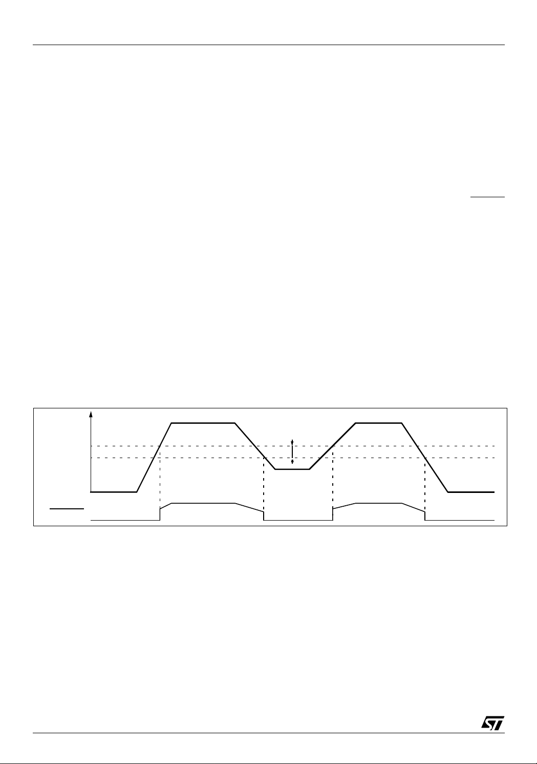
7.5.2.1 Monitoring the V
Main Supply
DD
The AVD vol tage t hreshold v alue is rel ative to t he
selected LVD threshold configured by option b yte
(see section 15.1 on page 109).
If the AVD interrupt is enabled, an interrupt is generated when the voltag e crosses the V
V
IT-(AVD)
threshold (AVDF bit is set).
IT+(LVD)
or
In the case of a drop in voltage, the AVD i nterrupt
acts as an early warning, allowing software to shut
down safely before the LVD re sets the microcontroller. See Figure 19.
The interrupt on the rising edge is used to inform
the application that the V
warning state is over
DD
Figure 19. Using the AVD to Monitor V
V
DD
V
IT+(AVD)
V
IT-(AVD)
V
IT+(LVD)
V
IT-(LVD)
AVDF bit
AVD INTERRUPT
REQUEST
IF AVDIE bit = 1
LVD RESET
01RESET
INTERRUPT Cleared by
DD
Early Warning Interrupt
(Power has dropped, MCU not
not yet in reset)
V
hyst
reset
01
INTERRUP T Cleared by
hardware
30/122
1
 Loading...