

SGS Thomson Microelectronics ST755CN, ST755CDTR, ST755CD Datasheet
ST755
ADJUSTABLE INVERTING NEGATIVE OUTPUT
CURRENT MODE PWM REGULATORS
September 1998
■ 2.7VTO 11VINPUT TOADJUSTABLE
NEGATIVEOUTPUTCONVERSION
■ 1WGUARANTEED OUTPUTPOWER
(V
in
>4.5V,T≤70oC)
■ 68%TYP.EFFICENCY AT6V
■ VERYLOW QUIESCENTCURRENT: 1.2mA
IN ON MODE10µA IN SHUT DOWN MODE
■ SOFTSTART
■ VERYLOW NOISEOUTPUT
■ 160KHzFIXEDFREQUENCY OSCILLATOR
■ MIXEDBIPOLAR-CMOSTECHNOLOGY
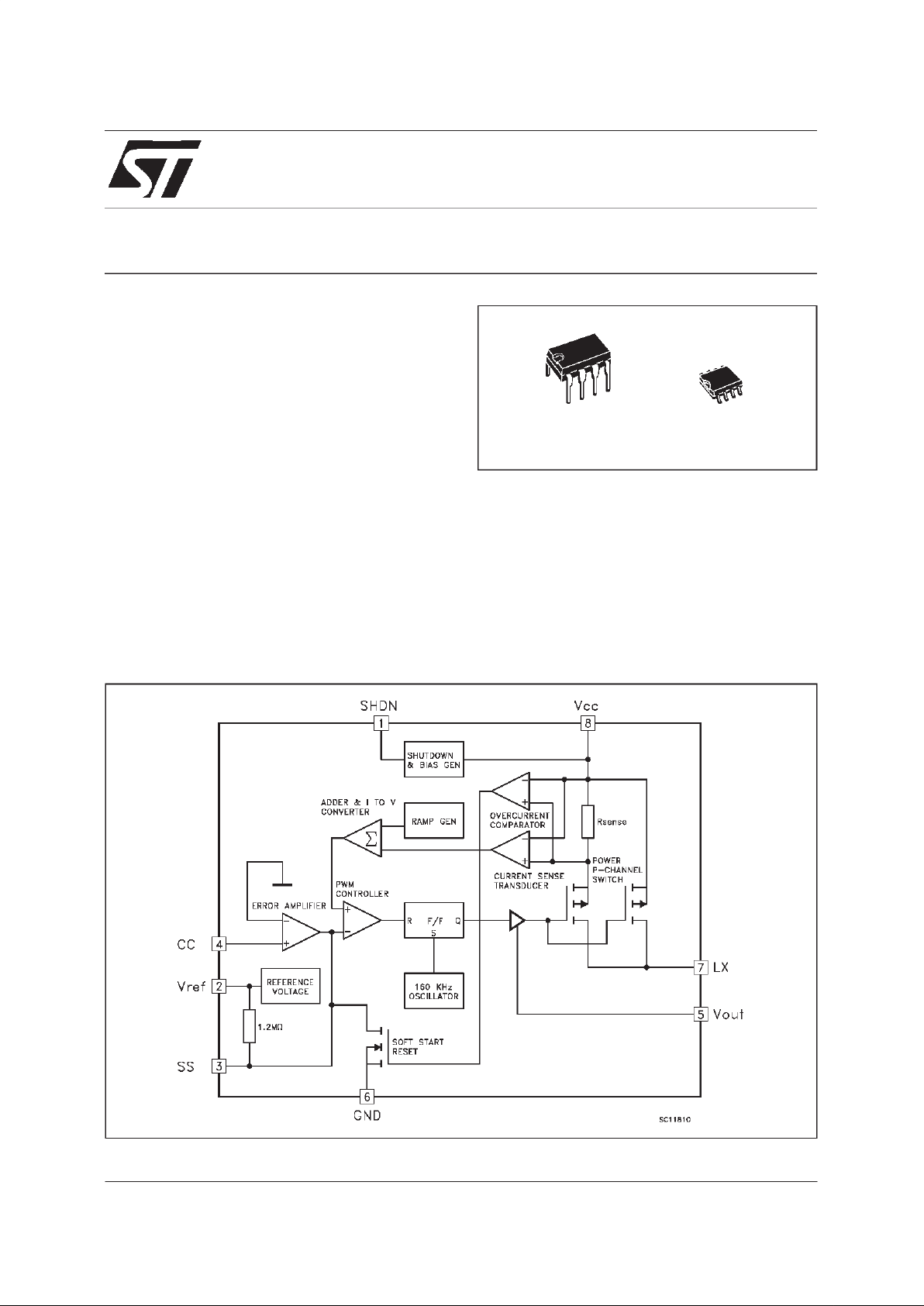
DESCRIPTION
The ST755 is an adjustable inverting
switch-mode DC-DC rergulator with internal
Power MOSFET that generaters an adjustable
negative output from a voltage input of 2.7V to
11V, output current guaranteed at 200mA (for
BLOCK DIAGRAM
DIP-8 SO-8
V
in
>4.5V, V
out
= -5V and 0oC ≤ Ta ≤ 70oC) and
275mA (typical value at T
a
=25oC, V
out
= -5V).
A logic controlled shut down pin that interfaces
directly with microprocessor reduces supply
current to only 10µA. Input to Output differential
voltage is limited to V
in
+|V
out
|<12.7V. No load
supplycurrent is 1.2mA.
1/9
Absolute Maximum Rating are those values beyond which damage to the device may occur.
Functional operation under these condition is not implied.
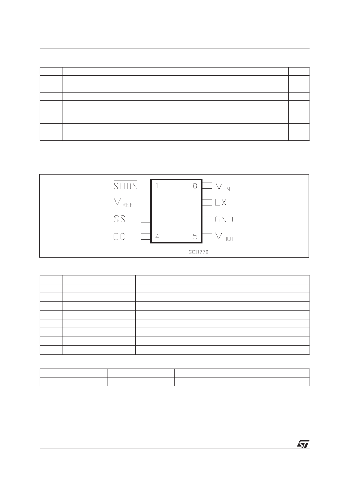
CONNECTION DIAGRAM AND (top view)
PINCONNECTIONS
Pin No Symbol Name and Function
1 SHDN SHUT-DOWNControl(V
CC
= On, GND=Shutdown)
2V
ref
Reference OutputVoltage (1.25V)
3 SS SoftStart
4 CC CompensationInput
5V
out
NegativeOutputVoltage
6 GND Ground
7 LX SwitchOutput
8V
CC
Positive Supply-Voltage Input
ORDERING NUMBERS
Type DIP-8 SO-8 (Tube) SO-8 (T&R)
ST755 ST755CN ST755CD ST755CD-TR
ABSOLUTE MAXIMUM RATINGS
Symbol Parameter Value Unit
V
cc
DC InputVoltage to GND -0.3 to 12 V
SHDN ShutdownVoltage -0.3 to V
CC
+0.3 V
Other InputVoltage -0.3 to V
CC
+0.3 V
I
LX
PeakSwitchCurrent 2 A
P
tot
Power Dissipation (at70oC) (for DIP-8)
(for SO-8)
725
470
mW
T
op
Operating Ambient Temperature Range -40 to 85
o
C
T
stg
StorageTemperature Range -55 to 150
o
C
ST755
2/9

ELECTRICAL CHARACTERISTICS (Refer to the test circuits, VCC= 5V, V
out
= -5.25 to -4.75V,
I
load
=0mA, Ta=T
min
to T
max
unless otherwise specified.Typical Value are referred at Ta=25oC)
Symbol Parameter Test Conditions Min. Typ. Max. Unit
V
IN
InputVoltage 2.7 11 V
V
o
OutputVoltage Io=0mAto200mA VCC= 4.5 to 6.2V -5.25 -5 -4.75 V
I
o
OutputCurrent VCC= 4.5 to 6.2V Ta=0oCto70oC
V
CC
= 4.5 to 6.2V Ta= -40oCto85oC
V
CC
=4V V
out
=-5V
V
CC
= 2.7 V V
out
=-5V
200
175
275
175
125
mA
mA
mA
mA
I
SUPPL Y
Supply Current(Including
Switching Current)
No Load, V
SHDN=VCC
1.2 3.5 m A
I
OFF
StandbyCurrent NoLoad, V
SHDN
=0V 10 100 µA
I
SC
ShortCircuit Current 1.2 A
∆V
o
LineRegulation VCC= 4 to 6.2V 0.1 %/V
∆V
o
LoadRegulation Io= 0mA to200mA 0.003 %/m A
V
REF
Reference Voltage Ta=25oC 1.18 1.25 1.32 V
∆V
REF
Reference Dritft Ta=T
min
toT
max
50 ppm /oC
R
DSON
LX OnResistance 0.7 Ω
I
LEAK
LX Leakage Current VDS=10V 1 µA
I
SH
Shutdown Pin Current 1 µA
V
il
Shutdown Input Low Threshold 0.25 V
V
ih
Shutdown Input High
Threshold
2V
f
o
OscillatorFrequency 160 KHz
ν Power Efficency I
o
= 100 mA 68 %
CC Compensation Pin Impedance 7.5 KΩ
Do not overload or short the Output to Ground. If the above conditions are observerd, the device may be damaged.
APPLICATION INFORMATION
The ST755 is an IC developed for voltage
conversion from an input voltage ranging from
+2.4V to 11V to a regulated adjustable negative
output limited by |V
out
| ≤ 12.7V-VIN. The circuit
adopts a current-mode PWM control scheme to
achieve good efficiency , high stability and low
noise performance. The figure in the first page
shown the detailed block diagram of the device.
ST755 is realized in a BCD technology in orderto
achieve high temperature stability, the best
REFERENCE precision , a very low quiescent
current and jitter free operations. The final stage
is built around a 0.7Ω - 2A P-Channel Power
MOS. A fraction of the output current is splitted
out for current detection.Internalclock frequency
is fixed to 160KHz. Error amplifier drives the
PWM comparator in order to keep 0V on the CC
input. So R
3
and R4resistors are calculated by
the following formulae R
4
= (|V
out
|/V
ref
)*R3(see fig
1). For R
3
can be choosen any value between
2KΩ and 20KΩ. Soft-Start (SS) input is a voltage
dependent-output current limit (see figure 9,
Switch Current Limit vs. SS Input Voltage). SS
pin is internally pulled to V
ref
through a 1.2 MΩ
resistor. Applying an appropiate capacitor at SS
input is possible to obtain a soft-start current
limitationduring power up. Forcing Soft-Start(SS)
input to a lower voltage through a resistive
voltage driver (R
1
and R2), the maximum LX
curent limit can be lowered according the
diagram showed in figure 9. When SHDN input is
low, the total current consumption is reduced to
10µA.
ST755
3/9
 Loading...