

V.90 USB WORLD MODEM CONTROLLER
GENERAL
.
USB HOT PLUG & PLAY INTERF A CE
.
DIRECT INTERFACE TO ST MAFE+DAA
CHIP-SET ST75951/ST952 FOR WORLDWIDE DAA DESIGN OR TO STLC7550 FOR
TRADITIONAL DAA DESIGN
.
WINDOWS 98 AND NT 5.0 SUPPORT
.
TA P I 2.0 COMPLIANT
.
SOFTWARE UPGRADABLE
.
MINIMUM SYSTEM REQUIREMENTS:
.
USB MOTHERBOARD, 166MHz PENTIUM
PROCESSOR WITH MMX TECHNOLOGY,
WINDOWS 98 AND 16MBYTES RAM OR
WINDOWS NT 5.0 AND 32MBYTES R AM
DEVICE F EATURE S
.
SINGLE 9.216MHz CRYSTAL OSCILLATOR
.
INTEGRATED ANALOG AND DIGITAL 3.3V
REGULATORS
.
DEDICATED PINS FOR RING, OFF-HOOK,
CLID, LOOP CURRENT SENS E
.
0.5µm CMOS PROCESS
.
TQFP48 (7 x 7 mm) PACKAGE
DATA MO DEM / FA X / VO ICE
.
V.90
.
V.34BIS, V.34, V.32BIS, V.32, V.22BIS, V.22,
V.23, V.21
.
BELL 103 AND BELL 212A
.
V.17, V.27TER, V.29, FAX CLASS 1 SUPP OR T
.
V.42, V.42BIS, MNP 2, 3, 4, 5
.
V.80
.
V .8 AND AUT O MODE
.
VOICE / FAX / MODEM DISTINCTION
.
ADPCM VOICE COMPRESSION/DECOMPRESSION
.
VOICE DETECTION (SILENCE DETECTION)
OTHER FEATURES
.
VIRTUAL UART (460.8Kbps)
.
AT HAYES COMMAND COMPATIBLE
.
TIME INDEPENDENT ESCAPE SEQUENCE
(TIES) COMMAND
.
CALLER ID
ST7554
SUMMARY DATA
TQFP48 (7 x 7 x 1.40mm)
(Full Plastic Quad Flat Pack)
.
DTMF DETECTION AND GENERATION
.
WAKE UP ON RING
.
WORLD-WIDE PROGRAMMABLE SILICON
DAA SUPPORT FOR ST75951/ST952
MAFE+DAA CHIP-SET
UNIVERSAL SERIA L BUS
.
SPECIFICATION 1.0, 12MBps FULL SPEED
.
ON-CHIP U SB TRANS CEIVER WITH DIGIT AL PLL
.
COMMUNICATION DEVICE CLASS AND
VENDOR REQUES TS
.
BUS OR SELF POWERED APPLICATION
(PIN-PROGRAMMABLE)
.
ONNOW POWER MANAGEMENT (D0, D2, D3)
.
LOW POWER CONSUMPTION (SUSPEND
MODE D2), WHOLE APPLICATION BELOW
500µA
DESCRIPTION
The ST7 554 is a single chip hos t si gnal processing
Modem/f ax/voice c ontroller that suppo rts data rates
up to 56Kbp s. All data pump a nd pro tocol f unctio ns
are executed on the host PC’s processor. This
product has been developed in cooperation with
Smart Link Ltd, who ported "USB-Modio", its host
based M odem and s ystem so ftware in to S T syst em
and hardwar e platform. The ST7554 directly connects to ST h igh per forma nce M odem analog fr ontend (MAFE) STLC7550 or to the highly integrated
MAFE+ DAA ch ip-set ST75951/S T952. The ST7554
also features an Universal Serial Bus (USB) interface for direct connection to the host PC for maximum flexi bility and real plug & play oper ation.
ORDER CODE : ST7554TQF7
January 1999
This is advance information on a new product now in development or undergoing evaluation. Details are subject to change without notice.
1/11
ST7554
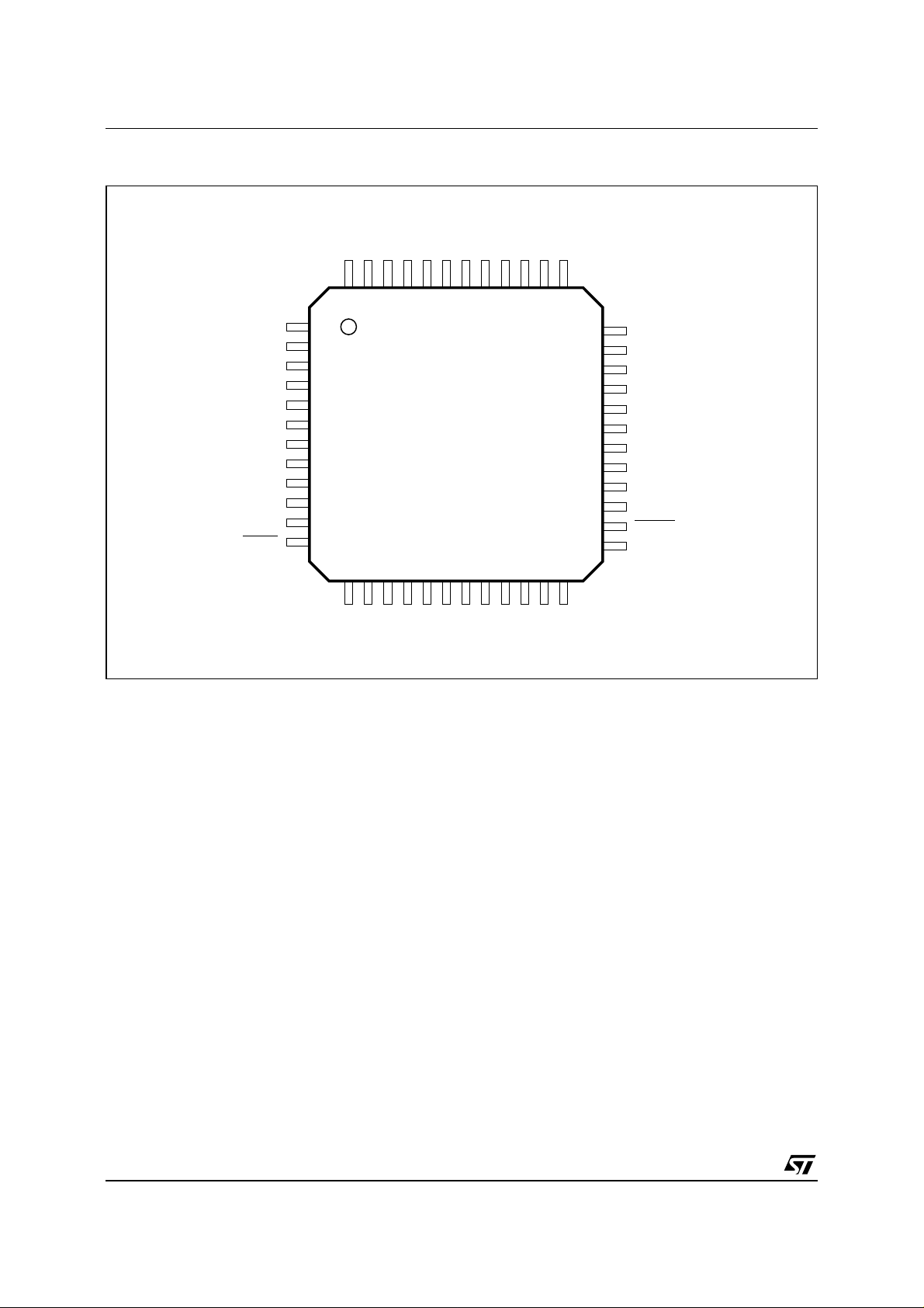
PIN CONNECTIONS
RESERVED
RI
47
48
HSDT
46
RESERVED
HO
44
45
BUZEN
PULSE
LED
41
RFC
40
DISHS
39
37
38
CLID
CD
42
43
D+
GNDBUS
VREGD
VBUS
VREGA
AGND
PSM
XTALIN
XTALOUT
FLTPLL
RESET
D-
1
2
3
4
5
6
7
8
9
10
11
12
15
14
13
RESERVED
RESERVED
RESERVED
16
1718192021
RESERVED
RESERVED
RESERVED
RESERVED
RESERVED
RESERVED
22
23
24
RESERVED
RESERVED
RESERVED
36
35
34
33
32
31
30
29
28
27
26
25
DC
TRxD
DAASEL
RESERVED
DGND
DOUT
DIN
MCLK
FS
HC1
PDOWN
RESERVED
7554S-01.EPS
2/11

PIN LIST
Name Pin Type Description
XTALIN 9 I Crystal Input
XTALOUT 10 O Crystal Output
RESET 12 I Reset Function to initialise the device (active low)
VBUS 5 I Positive Voltage Regulator Input, connected to USB VBUS
GNDBUS 3 I Regulator Ground, connected to USB Ground (0V) (see Note 1)
VREGA 6 I/O Positive Regulated Analog Input/Output Power Supply
VREGD 4 I/O Positive Regulated Digital Input/Output Power Supply
PSM 8 I Power Supply Mode (Bus-powered or Self-powered)
D+ 2 I/O Positive Data Signal of Differenti al Data Bus confor ming to USB Standard
D- 1 I/O Negative Data Signal of Differential Data Bus conforming to USB Standard
TRxD 35 I/O Transmit/Receive Data Led
DC 36 I/O DC mask
BUZEN 37 I/O Buzzer Amplifier Enable/Mute
PULSE 38 I/O Pulse dialing
DISHS 39 I/O Disconnect external phone
RFC 40 I/O Refresh
LED 41 I/O LED control
CD 42 I/O Carrier Detect Led
CLID 43 I/O Caller ID
HO 45 I/O Hook Control
HSDT 46 I/O Current sense
RI 48 I/O Ring Indicator
HC1 27 O Modem Codec Hardware Control mode selection
PDOWN 26 O SSI Powerdown bit output (active low)
MCLK 29 O SSI Master Clock Output
DAASEL 34 I Select Silicon or Discrete DAA Configuration Mode
FS 28 I SSI Frame Synchronisation Input
DOUT 31 O SSI Serial Data Output
DIN 30 I SSI Serial Data Input
FLTPLL 11 OA PLL filter analog output. Must be connected to analog ground AGND with
DGND 32 I Digital Ground (0V) (see Note 1)
AGND 7 I Analog Ground (0V) (see Note 1)
RESERVED 13 to 25-33-44 - Not connected
RESERVED 47 - Connect to digital ground DGND
Note 1 :
Analog and digital ground pins must be tied together to USB ground GNDBUS.
Specification 1.0
Specification 1.0
33pF capacitor
ST7554
7554S-01.TBL
3/11

ST7554
PIN DESCRIPTION
1 - Power Supply
1.1 - Regulator Input Power Supply
This pin must be connected to USB VBUS (+5V).
It supplies the integrated analog USB transceiver.
It is also the positive regulator power supply input
(5V) when ST7554 is in bus-powered mode
(PSM = 1) and it is used to internally generate the
3.3V supply for the digital and analog circuitry.
1.2 - Regulated Analog V
This pin is the analog power supply input (PSM = 0)
or analog 3.3V power supply output (PSM = 1).
This pin is the positive analog power supply for the
external Codec and DAA.
It is recommended to add a 1µF capacitor between
VREGA and GNDA as close as possible to the
IC pins.
1.3 - Regulated V
This pin is the digital power supply input (PSM = 0)
or digital 3.3V power supply output (PSM = 1).
This pin is the positive digital power supply for the
external Codec and DAA.
It is recommended to add a 1µF capacitor between
VREGA and GNDA as close as possible to the
IC pins.
1.4 - Power Supply Mode
This pin controls the VREGD and VREGA power
supply mode.
When PSM = 1, the application is bus-powered.
The 3.3V power supply is generated internally from
VBUS. In this case VREGD and VREGA are outputs which can be used to supply 3.3V to external
devices (see Figure 1).
When PSM = 0, the application is self-powered.
VBUS must be still connected to the VBUS Pin of
the USB connector in order to supply the integrated
USB transceiver . Anyway in this case VREGD and
VREGA mus t be fed by a 3.3V externally regulated
digital and analog power supplies (see Figure 2).
(7 pins)
Supply
DD
Supply
DD
(VREGD)
(PSM)
(VBUS)
(VREGA)
Figure 1 :
from USB
to other
digital ICs
to other
analog ICs
Figure 2 :
from USB
from 3.3V
externally
regulated
supplies
ST7554 in Bus-Powered mode
(PSM = 1)
ST7554
PSM
8
VBUS
5
GNDBUS
3
VREGD
4
DGND
32
VREGA
6
AGND
7
ST7554 in Self Powered mode
(PSM = 0)
ST7554
PSM
8
VBUS
5
GNDBUS
3
VREGD
4
DGND
32
VREGA
6
AGND
7
7554S-02.EPS
7554S-03.EPS
1.5 - Ground
(DGND, AGND and GNDB US)
DGND, AGND and GNDBUS are the digital, analog
and USB ground return pins respectively.
They should be connected together outside the
chip to the GND pin of the USB plug.
4/11
2 - USB Interface
(D+ , D-)
These pins are the positive and negative USB
differential data lines. They shall be both connected
to the USB plug or USB protection circuit via 27
Ω
series resistors for line impedance matching.
 Loading...