


POWER LINE FSK TRANSCEIVER
■ HALF DUPLEX FREQUENCY SHIFT KEYING
(FSK) TRANSC EIVER
■ INTEGRATED POWER LINE DRIVER WITH
PROGRAMMABLE VOLTAGE AND CURRENT
CONTROL
■ PROGRAMMABLE INTERFACE:
– SYNCHRONOUS
– ASYNCHRONOUS
■
SINGLE SU PPLY VOLTA GE (FR OM 7.5 UP TO 12.5V)
■
VERY LOW POWER CONSUMPTION (I q=5 mA)
■ INTEGRATED 5V VOLTAGE REGULATOR
(UP TO 100mA) WITH SHORT CIRCUIT
PROTECTION
■ 8 PROGRAMMABLE TRANSMISSION
FREQUENCIES
■
PROGRAMMABLE BAUD RATE UP TO 4800BPS
■ RECEIVING SENSITIVITY 1 mVRMS
■
SUITABLE TO APPLICATION IN ACCORDANCE
WITH EN 50065 CENELEC SPECIFICATIONS
■ CARRIER OR PREAMBLE DETECTION
■ BAND IN USE DETECTION
■ PROGRAMMABLE REGISTER WITH
SECURITY CHECKSUM
■ MAINS ZERO CROSSING DETECTION AND
SYNCHRONIZATION
ST7538
TQFP44 Slug Down
ORDERING NUMBER: ST7538P
■ WATCHDOG T IME R
DESCRIPTION
The ST7538 is a Half Duplex synchronous/asynchronous FSK Modem designed for power line
communication network applications. It operates
from a single supply voltage an d integrates a l ine
driver and a 5V linear regulator. The device operation is controlled by means of an internal register,
programmable through the syn chronous serial interface. Additional functions as watchdog, clock
output, output voltage and current control, preamble detection, time-out, band in use are i ncluded.
Realized in Multipower BCDV technology that allows to integrate DMOS, Bipolar and CMOS structures i n the same ch ip .
BLOCK DIAGRAM
CD/PD
RxD
CLR/T
REG/DA TA
RxTx
TxD
REGOK
September 2003
INTERFACE
XOut WD TOUT RSTO MCLK ZCin ZCout C_OUT CMINUS CPLUSXIn
SERIAL
CARRIER
DETECTION
PLL
TIME BASE
DIGITAL
FILTER
CONTROL
REGISTER
FSK
MODULAT OR
TEST
FSK
DEMODIFFILTER
DAC
ZCOSC
TEST3TEST1AVddDVdd AVssDVss BU
TX
FILTER
OP-AMP
+
-
RxFoTEST2
BU
FILTER
ALC
AGC
AMPL
CURRENT
CONTROL
VOLTAGE
CONTROL
PLI
VREG
FILTER
RAI
CL
Vsense
ATO
AT OP1
AT OP2
PAVcc
Vdc
PG
D03IN1407
1/30

ST7538
PIN CONNECTION (Top vi ew)
CD_PD
DVSS
RXD
RxTx
TXD
GND
TOUT
CLR/T
BU
DVDD
MCLK
C_MINUS
C_PLUS
N.C.
C_OUT
GND
PG
REG_DATA
N.C.
44 43 42 41 3940 38 37 36 35 34
1
2
3
4
5
6
7
8
9
10
12 13 14 15 16
171118 19 20 21 22
TEST1
REG_OK
N.C.
33
32
31
30
29
28
27
26
25
24
23
VDC
RAI
RXFO
TEST2
VSENSE
AVDD
XIN
XOUT
SGND
ATO
CL
RSTO
WD
TEST3
ZCIN
ZCOUT
N.C.
DVSS
ATOP1
PAVSS
ATOP2
D01IN1312
PAVCC
PIN DESCRIPTION
N° Name Type Description
1 CD_PD Digital/Output Carrier or Preamble Detect Output.
"1" No Carrier or Preamble Detected
"0" Carrier or Preamble Detected
2 DVss Supply Digital Ground
3 RxD Digital/Output RX Data Output.
4 RxTx Digital/Input
with internal pull-up
5 TxD Digital/Input
with internal pull-down
6 GND Supply Substrate Ground (same function as PIN 41)
7 TOUT Digital/Output TX Time Out Event Detection
8 CLR/T Digital/Output Synchronous Mains Access Clock or
9 BU Digital/Output Band in use Output.
10 DVdd Su pply Digital Supp ly Voltage
11 MCLK Digital/Output Master Clock Output
12 RSTO Digital/Output Power On or Watchdog Reset Output
13 TEST 3 Digital/Input
with internal pull-down
Rx or Tx mode selection input.
"1" - RX Session
"0" - TX Session
TX Data Input.
"1" - Time Out Event Occurred
"0" - No Time-out Event Occurred
Control Register Access Clock
"1" Signal within the Programmed Band
"0" No Signal within the Programmed Band
Test Input. Must be connected to DVss during Normal Operation
2/30
PIN DESCRIPTION (continued)
N° Name Type Description
14 WD Digital/Input
with internal pull-up
15 ZCOUT Digital/Output Zero Crossing Detection Output
16
ZCIN
1
Analog/Input Zero Crossing AC Input.
17 NC Floating Must be connected to DVss.
18 DVss Supply Digital Ground
19 ATOP1 Power/Output Power Line Driver Output
20 PAVss Supply Power Analog Ground
21 ATOP2 Power/Output Power Line Driver Output
22 PAV
23
CL
Supply Power Supply Voltage
CC
2
Analog/Input Current Limiting Feedback.
24 ATO Analog/Output Small Signal Analog Transmit Output
25 SGND Supply Analog Signal Ground
26 XOUT Analog I/O Crystal Output- External Clock Input
27 XIN Analog Input Crystal Oscillator Input
28 AVdd Supply Analog Power supply.
29
Vsense
3
Analog/Input Output Voltage Sensing input for the voltage control loop
30 TEST2 Analog/Input Test Input must be connected SGND
31 RxFO Analog/Output Receiving Filter Output
32 RAI Analog/Input Receiving Analog Input
33 VDC Power 5V Voltage Regulator Output
34 NC floating Must Be connected to DVss.
35 TEST1 Digital/Input
with internal pull-down
36 REGOK Digital/Output Security checksum logic output
37
38
C_MINUS
C_PLUS
4
Analog/Input Op-amp Inverting Input.
5
Analog/Input Op-amp Not Inverting Input.
39 NC floating Must Be connected to DVss
40 C_OUT Analog/Output Op-amp Output
41 GND Supply Substrate Ground (same function as PIN 6)
42 PG Digital/Output Power Good logic Output
43
REG_DATA
Digital/Input
with internal pull-down
44 NC floating Must be connected to DVss.
<1> If not used this pin must be connected to VDC
<2> Cannot be left floating
<3> Cannot be left floating
<4> If not used this pin must be connected to VDC
<5> If not used this pin must be tied low (SGND or PAVss or DVss)
Watchdog input. The Internal Watchdog Counter is cleared on the
falling edges.
A resistor between CL and AVss sets the PLI Current Limiting Value
Test input. Must Be connected to DVss.
"1" - Stored data Corrupted
"0" - Stored data OK
"1" - VDC is above 4.5V
"0" - VDC is below 4.25V
Mains or Control Register Access Selector
"1" - Control Register Access
"0" - Mains Access
ST7538
3/30
ST7538
ABSOLUTE MAXIMUM RATINGS
Symbol Parameter Value Unit
PAV
AV
DV
AV
/DVss Voltage between AVss and DVss -0.3 to +0.3 V
ss
V
V
O
I
O
V
sense
RAI Voltage Range at RAI Input -AV
ATO Output Current at ATO Output -2 to +2 mA
ATO Voltage range at ATO Output AV
ATOP1,2 Voltage range at Powered ATO Output AV
ATOP Powered ATO Output Current 400 mARms
T
amb
T
stg
ATOP1 Pin Maximum Withstanding Voltage Range
ATOP2 Pin ±1000 V
Other pins ±2000 V
Power Supply Voltage -0.3 to +14 V
CC
Analog Supply Voltage -0.3 to +5.5 V
dd
Digital Supply Voltage -0.3 to +5.5 V
dd
Digital input Voltage DVss - 0.3 to DVdd +0.3 V
I
Digital output Voltage DVss - 0.3 to DVdd +0.3 V
Digital Output Current -2 to +2 mA
Voltage Range at Vsense Input AVss - 0.3 to AVdd+0.3 V
- 0.3 to AVdd +0.3 V
dd
- 0.3 to AVdd +0.3 V
ss
- 0.3 to +PAVcc +0.3 V
ss
Operating ambient Temperature -40 to +85 °C
Storage Temperature -50 to 150 °C
±1500 V
Test Condition: CDF-AEC-Q100-002- “Human Body Model”
Acceptance Criteria: “Normal Performance”
THERMA L D ATA
Symbol Parameter
R
th-j-amb1
R
th-j-amb2
(*) Mou nted on Mu l t i l a y e r P CB with a dissipating sur face on th e bo t tom sid e of the PCB
(**) It's the s am e conditio n of the point ab ove, withou t any heatsi nking surface on the board.
Maximum Thermal Resistance Junction-Ambient Steady State(*) 35 °C/W
Maximum Thermal Resistance Junction-Ambient Steady State(**) 50 °C/W
TQFP44
with slug
Unit
4/30

ST7538
ELECTRICAL CHARACTERISTCS
(AVcc = DVcc = +5V, PAVcc =+9 V, PAVss, SGND = DVss = 0V,-40°C ≤ Tamb ≤ 85°C, unless otherwise specified)
Symbol Parameter Test Condition Min. Typ. Max. Unit
AV
,
Supply Voltages 4.75 5 5.25 V
CC
DV
CC
PAVCC - DVCCPAVCC and DVCC Relation
during Power-Up Sequence
PAVCC - AVCCPAVCC and DVCC Relation
during Power-Up Sequence
PAV
Power Supply Voltage 7.5 12.5 V
cc
Max allowed slope during
Power-Up
AICC + DICC Input Supply Current Transmission & Receiving mode 5 7 mA
I PAV
Powered Analog Supply
CC
Current
Digital I/O
V
V
V
OH
V
OL
High Logic Level Input Voltage 2 V
IH
Low Logic Level input Voltage 0.8 V
IL
High Logic Level Output Voltage IOH= -2mA 3.5 V
Low Logic Level Output Voltage IOL= 2mA 0.4 V
Oscillator
V
IHX
V
ILX
XIN High Level Input Voltage External Clock 3 V
XIN Low Level Input Voltage External Clock 2 V
DC XTAL Clock Duty Cycle External Clock 40 60 %
Xtal Crystal Oscillator frequency 16 MHz
Tclock Oscillator Period (1/Xtal) 62.5 ns
Xtal
External Oscillator Esr
ESR
Resistance
Xtal
External Oscillator Stabilization
CL
Capacitance
Transmitter
IATOP Output Transmitting Current in
programmable current limiting
V
V
ATODC
HD2
ATO
Max Carrier Output AC Voltage RCL = 1.85kΩ Vsense=0V 1.75 2.3 3.5 V
Output DC Voltage on ATO 1.7 2.1 2.5 V
Second Harmonic Distortion on
ATO
ATO
HD3
Third Harmo nic Distortion on
ATO
ATO
V
ATOP (AC)
Max Carrier Output AC Voltage
for each ATOP1 and ATOP2
pins
V
ATOP(DC)
Output DC Voltage on ATOP1
and ATOP2 pins
DVCC < 4.75V 0.1 1.2 V
AVCC < 4.75V 0.1 1.2 V
10 V/ms
TX mode (no load) 30 50 mArms
RX mode 500 1000 µA
Maximum total current 370 mArms
40 Ohm
16 pF
Vsense connected though a
100pF cap to GND; Rcl=1.85kΩ;
=1Ω (as in fig. 13)
R
LOAD
V
= 2VPP; Fc=86KHz -55 -42 dB
ATO
V
= 2VPP; Fc=86KHz -52 -49 dB
ATO
RCL = 1.85kΩ
250 310 370 mArms
PP
3.5 4.6 6 V
pp
Vsense=0V
PAVcc
VATOP AC()
------------------------------------ 7.5V+≥
2
3.5 4.2 5 V
5/30

ST7538
ELECTRICAL CHARACTERISTCS
(AVcc = DVcc = +5V, PAVcc =+9 V, PAVss, SGND = DVss = 0V,-40°C
(continued)
≤
Tamb ≤ 85°C, unless otherwise specified)
Symbol Parameter Test Condition Min. Typ. Max. Unit
HD2
ATOP
Second Harmonic Distortion on
each ATOP1 and ATOP2 pins
V
= 4V
ATOP
No Load
V
= 4V
ATOP
R
=50Ω (Differential)
LOAD
PP
PP
-55 -42 dB
-65 -53 dB
Carrier Frequency: 132.5KHz
HD3
ATOP
Third Harmo nic Distortion on
each ATOP1 and ATOP2 pins
V
= 4V
ATOP
No Load.
V
= 4V
ATOP
R
=50Ω (Differential)
LOAD
PP
PP
-56 -49 dB
-65 -52 dB
Carrier Frequency: 132.5KHz
VATOP Accuracy with Voltage Control
R
= 0Ω -1 +1 GST
CL
Loop Active
GST ALC Gain Step Control loop
0.6 1 1.4 dB
gain step
DRNG ALC Dynamic Range 30 dB
VCL
VCL
TH
HYST
Voltage control loop reference
threshold on V
sense
pin
Hysteresis on Voltage loop
Figure 13 170 190 210 mV
Figure 13 +-19 mV
reference threshold
CCL
CCL
TH
HYST
Current control loop reference
threshold on C
sense
pin
Hysteresis on Voltage loop
Figure 13 1.80 1.90 2.00 V
Figure 13 210 250 290 mV
reference threshold
V
SENSE
T
RxTx
VSENSE Input Impedance 36 KΩ
Carrier Activation Time Figure 16 - 600 Baud Xtal=16MHz 0.01 1.6 ms
Figure 16- 1200 Baud
0.01 800 µs
Xtal=16MHz
Figure 16- 2400 Baud
0.01 400 µs
Xtal=16MHz
Figure 16- 4800 Baud
0.01 200 µs
Xtal=16MHz
TALC Carrier Stabilization Time
From STEP 16 to zero or From
Figure 16.
Xtal =16MHz
3.2 ms
step 16 to step 31,
T
ST
Tstep Figure 16
200 µs
Xtal =16MHz
Receiver
V
Input Sensitivity (Normal Mode) 1 2 mV
IN
Input Sensitivity (High Sens.) 5 00 µ
V
R
V
CD
Maximum Input Signal 2 V
IN
Input Impedance 80 100 140 kΩ
IN
Carrier Detection Sensitivity
12mV
(Normal Mode)
Carrier Detection Sensitivity
500 µ
(High Sensitivity Mode )
V
BU
Band in Use Detection Level 77 85 dB/
PK
rms
V
rms
rms
rms
V
rms
µVrms
6/30

ST7538
ELECTRICAL CHARACTERISTCS
(AVcc = DVcc = +5V, PAVcc =+9 V, PAVss, SGND = DVss = 0V,-40°C
(continued)
≤
Tamb ≤ 85°C, unless otherwise specified)
Symbol Parameter Test Condition Min. Typ. Max. Unit
Voltage Regulator
VDC Linear Regulator Output
Voltage
-25<Tj<125 C
0<Io<100mA
-25<Tj<125 C
4.9 5.05 5.2 V
4.7 5.2 V
0<Io<150mA
Line Regulation 7.5V<PAVcc<12.5V
10 50 mV
Idc=10mA
Load Regulation 5mA<Id c<100 mA
20 75 mV
Vin=7.5V
) Linear Regulator Current
I(V
DC
150 180 210 V
Limitation
UVLO Input Under Voltage Lock Out
3.7 3.9 4.1 V
Threshold
UVLO
PG Power Good Output Voltage
UVLO Hysteresis 340 mV
HYS
4.3 4.5 4.7 V
Threshold on VDC pin
PG
HYS
PG Hysteresis 250 mV
Other Functions
T
RSTO
T
T
WD
WM
Reset Time See Figure 18; Xtal=16MHz 50 ms
Watch-dog Pulse Width See Figure 18 3.5 ms
Watch-dog Pulse Period See Figure 18 T
WD
+
1490 ms
3.5
T
T
T
T
OFFD
T
WO
OUT
OFF
CD
Watch-dog Time Out See Figure 18 1.5 s
TX TIME OUT Control Register Bit 7 and Bit 8
See Figure 17
1
3
Time Out OFF Time See Figure 17 125 ms
RxTx 0->1 vs. TOUT Delay See Figure 17 20 µs
Carrier Detection Time
selectable by register
Control Register
bit 9 and bit10
Figure 10
500
1
3
5
T
M
B
DCD
CLK
AUD
CD_PD Propagation Delay Figure 10 300 500 µs
Master Clock Output
Selectable by register
Baud rate Control Register
Control Register
bit 15 and bit 16
see table 6
bit 3 and bit 4
see table 6
fclock
fclock/2
fclock/4
600
1200
2400
4800
T
Baud rate Bit Time (=1/
B
) Control Regis ter
BAUD
bit 3 and bit 4
see table 6
1667
833
417
208
Zero Crossing Detection
ZC
DEL
Zero Crossing Detection delay
Figure 19 1 µs
(delay between the ZCIN and
ZCOUT signals)
s
µs
ms
ms
ms
MHz
Baud
µs
7/30
ST7538
ELECTRICAL CHARACTERISTCS
(AVcc = DVcc = +5V, PAVcc =+9 V, PAVss, SGND = DVss = 0V,-40°C
(continued)
≤
Tamb ≤ 85°C, unless otherwise specified)
Symbol Parameter Test Condition Min. Typ. Max. Unit
ZC
(LOW)
Zero Crossing Detection Low
-45 -5 mV
Threshold
ZC
(HIGH)
Zero Crossing Detection High
5 +45 mV
Threshold
ZC
(OFFSET)
Zero Crossing Offset -20 +20 mV
Operational Amplifier
C
OUT(Sync)
C
OUT(Source)
C
IN(Offset)
Max Sync Current 15 28 45 mA
Max Source Current -30 -20 -10 mA
Input Terminals OFFSET -38 +38 mV
GBWP Gain Bandwidth Product 6 7 9 MHz
Serial Interface
Ts Setup Time see figure 3, 5, 6, 7 & 8 5 ns
T
T
T
T
T
T
CRP
CR
CC
DS
DH
Hold Time see figure 3, 5, 6, 7 & 8 2 ns
H
CLR/T vs. REG_DATA or RxTx see figure 3, 5, 6, 7 & 8 TB/4
CLR/T vs. CLR/T see figure 3, 5, 6, 7 & 8 T
B
Setup Time see figure 3, 5, 6, 7 & 8 TB/4 TB/2
Hold Time see figure 3, 5, 6, 7 & 8 TB/4 TB/2
see figure 4 T
H
2*T
TB/2
B
8/30
ST7538
FUNCTIONAL DESCRIPTION
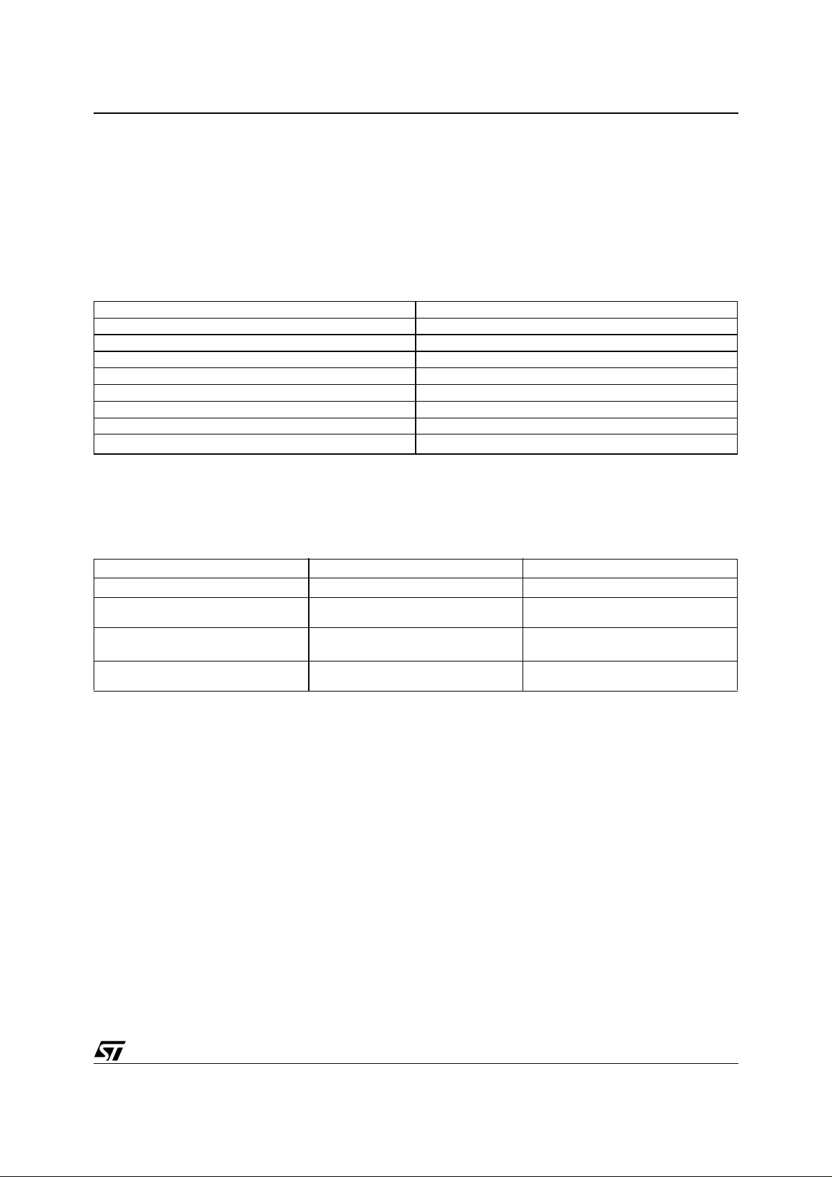
Carrier Frequencies
ST7538 is a multi frequency device: eight programmable Carrier Frequencies are available (see table 1).
Only one Carrier could be used a time. The communicat ion channel could be varied during the normal
working Mode to realize a multifrequency communication.
Selecting the desired frequency in the Control Register the Transmission and Reception filters are accordingly tuned.
Table 1.
FCarrier F (KHz)
F0 60
F1 66
F2 72
F3 76
F4 82.05
F5 86
F6 110
(1)
F7
Baud Rates
ST7538 is a multi Baud rate device: four Baud Rate are available (See table 2).
132.5
Table 2.
Baud Rate [Baud]
600 600
1200 600
2400
4800 2400
Note: 1. D efault value
2. Frequency deviation.
3. Deviation = ∆F / (Baud Rate)
4. Deviation 0.5 Not Allowed
(1)
(2)
(Hz) Deviation
∆F
1200
(1)
1200
2400
4800
(4)
1
0.5
1
0.5
1
0.5
1
(3)
9/30
 Loading...