

SGS Thomson Microelectronics ST72F264G2M6, ST72F264G2B6, ST72264G2M6, ST72264G2B6, ST72264G2 Datasheet
...
ST72260G, ST72262G,
ST72264G
8-BIT MCU WITH FLASH OR ROM MEM ORY,
ADC, TWO 16-BIT TIMERS, I
■ Memories
– 4 K or 8 Kby tes Program memory: ROM or
Single voltage extended Flash (XFlash) with
read-out protection write protection and InCircuit Programming and In-Application Programming (ICP and IAP). 10K write/erase cycles guaranteed, data retention: 20 years at
55°C.
– 256 bytes RAM
■ Clock, Re set and Supp ly Managem ent
– Enhanced reset system
– Enhanced low voltage supply supervisor
(LVD) with 3 programmable levels and auxiliary voltage detector (AVD) with interrupt capability for implementing safe power-down
procedures
– Clock sources: crystal/ceramic resonat or os-
cillators , internal RC os cillator, clock se curity
system and bypass for external clock
– PLL for 2x frequency multiplication
– Clock-out capability
– 4 Power Saving Modes: Halt, Active Halt,Wait
and Slow
■ Interrupt Management
– Nested interrupt controller
– 10 interrupt vectors plus TRAP and RESET
– 22 external interrupt lines (on 2 vectors)
■ 22 I/ O P o rts
– 22 multifunctional bidirectional I/O lines
– 20 alternate function lines
– 8 high sink outputs
■ 4 Timers
– Main Clock Controller with Real time base and
Clock-out capabilities
– Configurable watchdog timer
Device Summary
Features
Program memory - bytes 4K 4K 8K 4K 8K
RAM (stack) - bytes 256 (128)
Periphe rals
Operating Supply 2.4 V to 5.5 V
CPU Frequency Up to 8 MHz (with oscillator up to 16 MHz) PLL 4/8 Mhz
Operating Temperature -40° C to +85° C 0° C to +70° C
Packages SO28 / SDIP32 LFBGA
ST72260G1 ST72262G1 ST72262G2 ST72264G1 ST72264G2
Watchdog timer,
RTC,
Two16-bit timers,
SPI
Watchdog timer, RTC
Two 16-bit timers,
SPI, ADC
2
C, SPI, SCI INTERFACES
SDIP32
LFBGA 6x6mm
SO28
– Two 16-bit timers with: 2 input captures, 2 out-
put compares, external clock input on one timer, PWM and Pulse generator modes
■ 3 Communications Interfaces
– SPI synchronous serial interface
2
C multimaster interface
–I
– SCI asynchronous serial interface (LIN com-
patible)
■ 1 Analog peripheral
– 10-bit ADC with 6 input channels
■ Instruction Set
– 8-bit data manipulation
– 63 basic instructions
– 17 main addressing modes
– 8 x 8 unsigned multiply instruction
■ Development Tools
– Full hardware/software development package
Watchdog timer, RT C
Two 16-bit timers ,
SPI, SCI, I
2
C, ADC
Rev. 1.7
August 2003 1/171
1

Table of Contents
ST72260G, ST72262G,
ST7226 4G . . . . . . . . . . . . . . . . . . . . . . . . . . . . . . . . . . . . . . . . . . 1
1 INTRODUCTION . . . . . . . . . . . . . . . . . . . . . . . . . . . . . . . . . . . . . . . . . . . . . . . . . . . . . . . . . . . . . . 5
2 PIN DESCRIPTION . . . . . . . . . . . . . . . . . . . . . . . . . . . . . . . . . . . . . . . . . . . . . . . . . . . . . . . . . . . . 6
3 REGISTER & MEMORY MAP . . . . . . . . . . . . . . . . . . . . . . . . . . . . . . . . . . . . . . . . . . . . . . . . . . . 10
4 FLASH PROGRAM MEMORY . . . . . . . . . . . . . . . . . . . . . . . . . . . . . . . . . . . . . . . . . . . . . . . . . . 14
4.1 INTRODUCTION . . . . . . . . . . . . . . . . . . . . . . . . . . . . . . . . . . . . . . . . . . . . . . . . . . . . . . . 14
4.2 MAIN FEATURES . . . . . . . . . . . . . . . . . . . . . . . . . . . . . . . . . . . . . . . . . . . . . . . . . . . . . . 14
4.3 PROGRAMMING MODES . . . . . . . . . . . . . . . . . . . . . . . . . . . . . . . . . . . . . . . . . . . . . . . . 14
4.4 ICC INTERFACE . . . . . . . . . . . . . . . . . . . . . . . . . . . . . . . . . . . . . . . . . . . . . . . . . . . . . . . 15
4.5 MEMORY PROTECTION . . . . . . . . . . . . . . . . . . . . . . . . . . . . . . . . . . . . . . . . . . . . . . . . 16
4.6 REGISTER DESCRIPTION . . . . . . . . . . . . . . . . . . . . . . . . . . . . . . . . . . . . . . . . . . . . . . . 16
5 CENTRAL PROCESSING UNIT . . . . . . . . . . . . . . . . . . . . . . . . . . . . . . . . . . . . . . . . . . . . . . . . . 17
5.1 INTRODUCTION . . . . . . . . . . . . . . . . . . . . . . . . . . . . . . . . . . . . . . . . . . . . . . . . . . . . . . . 17
5.2 MAIN FEATURES . . . . . . . . . . . . . . . . . . . . . . . . . . . . . . . . . . . . . . . . . . . . . . . . . . . . . . 17
5.3 CPU REGISTERS . . . . . . . . . . . . . . . . . . . . . . . . . . . . . . . . . . . . . . . . . . . . . . . . . . . . . . 17
6 SUPPLY, RESET AND CLOCK MANAGEMENT . . . . . . . . . . . . . . . . . . . . . . . . . . . . . . . . . . . . 20
6.1 PHASE LOCKED LOOP . . . . . . . . . . . . . . . . . . . . . . . . . . . . . . . . . . . . . . . . . . . . . . . . . 20
6.2 MULTI-OSCILLATOR (MO) . . . . . . . . . . . . . . . . . . . . . . . . . . . . . . . . . . . . . . . . . . . . . . . 21
6.3 RESET SEQUENCE MANAGER (RSM) . . . . . . . . . . . . . . . . . . . . . . . . . . . . . . . . . . . . . 22
6.4 SYSTEM INTEGRITY MANAGEMENT (SI) . . . . . . . . . . . . . . . . . . . . . . . . . . . . . . . . . . 24
7 INTERRUPTS . . . . . . . . . . . . . . . . . . . . . . . . . . . . . . . . . . . . . . . . . . . . . . . . . . . . . . . . . . . . . . . 28
7.1 INTRODUCTION . . . . . . . . . . . . . . . . . . . . . . . . . . . . . . . . . . . . . . . . . . . . . . . . . . . . . . . 28
7.2 MASKING AND PROCESSING FLOW . . . . . . . . . . . . . . . . . . . . . . . . . . . . . . . . . . . . . . 28
7.3 INTERRUPTS AND LOW POWER MODES . . . . . . . . . . . . . . . . . . . . . . . . . . . . . . . . . . 30
7.4 CONCURRENT & NESTED MANAGEMENT . . . . . . . . . . . . . . . . . . . . . . . . . . . . . . . . . 30
7.5 INTERRUPT REGISTER DESCRIPTION . . . . . . . . . . . . . . . . . . . . . . . . . . . . . . . . . . . . 31
8 POWER SAVING MODES . . . . . . . . . . . . . . . . . . . . . . . . . . . . . . . . . . . . . . . . . . . . . . . . . . . . . 33
8.1 INTRODUCTION . . . . . . . . . . . . . . . . . . . . . . . . . . . . . . . . . . . . . . . . . . . . . . . . . . . . . . . 33
8.2 SLOW MODE . . . . . . . . . . . . . . . . . . . . . . . . . . . . . . . . . . . . . . . . . . . . . . . . . . . . . . . . . 33
8.3 WAIT MODE . . . . . . . . . . . . . . . . . . . . . . . . . . . . . . . . . . . . . . . . . . . . . . . . . . . . . . . . . . 34
8.4 ACTIVE-HALT AND HALT MODES . . . . . . . . . . . . . . . . . . . . . . . . . . . . . . . . . . . . . . . . 35
8.5 HALT MODE . . . . . . . . . . . . . . . . . . . . . . . . . . . . . . . . . . . . . . . . . . . . . . . . . . . . . . . . . . 36
9 I/O PORTS . . . . . . . . . . . . . . . . . . . . . . . . . . . . . . . . . . . . . . . . . . . . . . . . . . . . . . . . . . . . . . . . . . 38
9.1 INTRODUCTION . . . . . . . . . . . . . . . . . . . . . . . . . . . . . . . . . . . . . . . . . . . . . . . . . . . . . . . 38
9.2 FUNCTIONAL DESCRIPTION . . . . . . . . . . . . . . . . . . . . . . . . . . . . . . . . . . . . . . . . . . . . 38
9.3 I/O PORT IMPLEMENTATION . . . . . . . . . . . . . . . . . . . . . . . . . . . . . . . . . . . . . . . . . . . . 41
9.4 UNUSED I/O PINS . . . . . . . . . . . . . . . . . . . . . . . . . . . . . . . . . . . . . . . . . . . . . . . . . . . . . 41
9.5 LOW POWER MODES . . . . . . . . . . . . . . . . . . . . . . . . . . . . . . . . . . . . . . . . . . . . . . . . . . 41
9.6 INTERRUPTS . . . . . . . . . . . . . . . . . . . . . . . . . . . . . . . . . . . . . . . . . . . . . . . . . . . . . . . . . 41
9.7 DEVICE-SPECIFIC I/O PORT CONFIGURATION . . . . . . . . . . . . . . . . . . . . . . . . . . . . . 42
171
2/171
2

Table of Contents
9.8 I/O PORT REGISTER DESCRIPTION . . . . . . . . . . . . . . . . . . . . . . . . . . . . . . . . . . . . . . 43
10 MISCELLANEOUS REGISTERS . . . . . . . . . . . . . . . . . . . . . . . . . . . . . . . . . . . . . . . . . . . . . . . 45
10.1 I/O PORT INTERRUPT SENSITIVITY . . . . . . . . . . . . . . . . . . . . . . . . . . . . . . . . . . . . . . 45
10.2 I/O PORT ALTERNATE FUNCTIONS . . . . . . . . . . . . . . . . . . . . . . . . . . . . . . . . . . . . . . . 45
10.3 MISCELLANEOUS REGISTER DESCRIPTION . . . . . . . . . . . . . . . . . . . . . . . . . . . . . . . 46
11 ON-CHIP PERIPHERALS . . . . . . . . . . . . . . . . . . . . . . . . . . . . . . . . . . . . . . . . . . . . . . . . . . . . . 48
11.1 WATCHDOG TIMER (WDG) . . . . . . . . . . . . . . . . . . . . . . . . . . . . . . . . . . . . . . . . . . . . . . 48
11.2 MAIN CLOCK CONTROLLER WITH REAL TIME CLOCK (MCC/RTC) . . . . . . . . . . . . . 53
11.3 16-BIT TIMER . . . . . . . . . . . . . . . . . . . . . . . . . . . . . . . . . . . . . . . . . . . . . . . . . . . . . . . . . 55
11.4 SERIAL PERIPHERAL INTERFACE (SPI) . . . . . . . . . . . . . . . . . . . . . . . . . . . . . . . . . . . 74
11.5 SERIAL COMMUNICATIONS INTERFACE (SCI) . . . . . . . . . . . . . . . . . . . . . . . . . . . . . . 85
11.6 I2C BUS INTERFACE (I2C) . . . . . . . . . . . . . . . . . . . . . . . . . . . . . . . . . . . . . . . . . . . . . . 99
11.7 10-BIT A/D CONVERTER (ADC) . . . . . . . . . . . . . . . . . . . . . . . . . . . . . . . . . . . . . . . . . 112
12 INSTRUCTION SET . . . . . . . . . . . . . . . . . . . . . . . . . . . . . . . . . . . . . . . . . . . . . . . . . . . . . . . . 116
12.1 CPU ADDRESSING MODES . . . . . . . . . . . . . . . . . . . . . . . . . . . . . . . . . . . . . . . . . . . . 116
12.2 INSTRUCTION GROUPS . . . . . . . . . . . . . . . . . . . . . . . . . . . . . . . . . . . . . . . . . . . . . . . 119
13 ELECTRICAL CHARACTERISTICS . . . . . . . . . . . . . . . . . . . . . . . . . . . . . . . . . . . . . . . . . . . . 122
13.1 PARAMETER CONDITIONS . . . . . . . . . . . . . . . . . . . . . . . . . . . . . . . . . . . . . . . . . . . . . 122
13.2 ABSOLUTE MAXIMUM RATINGS . . . . . . . . . . . . . . . . . . . . . . . . . . . . . . . . . . . . . . . . 123
13.3 OPERATING CONDITIONS . . . . . . . . . . . . . . . . . . . . . . . . . . . . . . . . . . . . . . . . . . . . . 124
13.4 SUPPLY CURRENT CHARACTERISTICS . . . . . . . . . . . . . . . . . . . . . . . . . . . . . . . . . . 127
13.5 CLOCK AND TIMING CHARACTERISTICS . . . . . . . . . . . . . . . . . . . . . . . . . . . . . . . . . 130
13.6 MEMORY CHARACTERISTICS . . . . . . . . . . . . . . . . . . . . . . . . . . . . . . . . . . . . . . . . . . 135
13.7 EMC CHARACTERISTICS . . . . . . . . . . . . . . . . . . . . . . . . . . . . . . . . . . . . . . . . . . . . . . 136
13.8 I/O PORT PIN CHARACTERISTICS . . . . . . . . . . . . . . . . . . . . . . . . . . . . . . . . . . . . . . . 141
13.9 CONTROL PIN CHARACTERISTICS . . . . . . . . . . . . . . . . . . . . . . . . . . . . . . . . . . . . . . 147
13.10 TIMER PERIPHERAL CHARACTERISTICS . . . . . . . . . . . . . . . . . . . . . . . . . . . . . . . . . 148
13.11 COMMUNICATION INTERFACE CHARACTERISTICS . . . . . . . . . . . . . . . . . . . . . . . . 149
13.12 10-BIT ADC CHARACTERISTICS . . . . . . . . . . . . . . . . . . . . . . . . . . . . . . . . . . . . . . . . 152
14 PACKAGE CHARACTERISTICS . . . . . . . . . . . . . . . . . . . . . . . . . . . . . . . . . . . . . . . . . . . . . . 154
14.1 PACKAGE MECHANICAL DATA . . . . . . . . . . . . . . . . . . . . . . . . . . . . . . . . . . . . . . . . . 154
14.2 THERMAL CHARACTERISTICS . . . . . . . . . . . . . . . . . . . . . . . . . . . . . . . . . . . . . . . . . 155
14.3 SOLDERING AND GLUEABILITY INFORMATION . . . . . . . . . . . . . . . . . . . . . . . . . . . . 156
15 DEVICE CONFIGURATION AND ORDERING INFORMATION . . . . . . . . . . . . . . . . . . . . . . . 157
15.1 OPTION BYTES . . . . . . . . . . . . . . . . . . . . . . . . . . . . . . . . . . . . . . . . . . . . . . . . . . . . . . 157
15.2 DEVICE ORDERING INFORMATION AND TRANSFER OF CUSTOMER CODE . . . . 159
15.3 DEVELOPMENT TOOLS . . . . . . . . . . . . . . . . . . . . . . . . . . . . . . . . . . . . . . . . . . . . . . . 161
15.4 ST7 APPLICATION NOTES . . . . . . . . . . . . . . . . . . . . . . . . . . . . . . . . . . . . . . . . . . . . . 163
16 SUMMARY OF CHANGES . . . . . . . . . . . . . . . . . . . . . . . . . . . . . . . . . . . . . . . . . . . . . . . . . . . 165
ERRATA SHEET . . . . . . . . . . . . . . . . . . . . . . . . . . . . . . . . . . . 166
3
3/171

ST72260G, ST72262G, ST72264G
17 SILICON IDENTIFICATION . . . . . . . . . . . . . . . . . . . . . . . . . . . . . . . . . . . . . . . . . . . . . . . . . . . 166
18 REFERENCE SPECIFICATION . . . . . . . . . . . . . . . . . . . . . . . . . . . . . . . . . . . . . . . . . . . . . . . 166
19 SILICON LIMITATIONS . . . . . . . . . . . . . . . . . . . . . . . . . . . . . . . . . . . . . . . . . . . . . . . . . . . . . 166
19.1 EXECUTION OF BTJX INSTRUCTION . . . . . . . . . . . . . . . . . . . . . . . . . . . . . . . . . . . . 166
19.2 I/O PORT B AND C CONFIGURATION . . . . . . . . . . . . . . . . . . . . . . . . . . . . . . . . . . . . 166
19.3 16-BIT TIMER PWM MODE . . . . . . . . . . . . . . . . . . . . . . . . . . . . . . . . . . . . . . . . . . . . . 167
19.4 SPI MULTIMASTER MODE . . . . . . . . . . . . . . . . . . . . . . . . . . . . . . . . . . . . . . . . . . . . . 167
19.5 MINIMUM OPERATING VOLTAGE . . . . . . . . . . . . . . . . . . . . . . . . . . . . . . . . . . . . . . . 167
19.6 CSS FUNCTION . . . . . . . . . . . . . . . . . . . . . . . . . . . . . . . . . . . . . . . . . . . . . . . . . . . . . . 167
19.7 INTERNAL AND EXTERNAL RC OSCILLATOR WITH LVD . . . . . . . . . . . . . . . . . . . . 167
19.8 EXTERNAL CLOCK WITH PLL . . . . . . . . . . . . . . . . . . . . . . . . . . . . . . . . . . . . . . . . . . . 167
19.9 HALT MODE POWER CONSUMPTION WITH ADC ON . . . . . . . . . . . . . . . . . . . . . . . 168
19.10 ACTIVE HALT WAKE-UP BY EXTERNAL INTERRUPT . . . . . . . . . . . . . . . . . . . . . . . 168
19.11 A/D CONVERTER ACCURACY FOR FIRST CONVERSION . . . . . . . . . . . . . . . . . . . . 168
19.12 NEGATIVE INJECTION IMPACT ON ADC ACCURACY . . . . . . . . . . . . . . . . . . . . . . . 168
19.13 ADC CONVERSION SPURIOUS RESULTS . . . . . . . . . . . . . . . . . . . . . . . . . . . . . . . . . 168
19.14 FUNCTIONAL EMS . . . . . . . . . . . . . . . . . . . . . . . . . . . . . . . . . . . . . . . . . . . . . . . . . . . . 169
20 DEVICE MARKING . . . . . . . . . . . . . . . . . . . . . . . . . . . . . . . . . . . . . . . . . . . . . . . . . . . . . . . . . 169
21 ERRATA SHEET REVISION HISTORY . . . . . . . . . . . . . . . . . . . . . . . . . . . . . . . . . . . . . . . . . 170
To obtain the most recent version of this datasheet,
please check at www.st.com>products>technical literature>datasheet
Please note that an errata sheet can be found at the end of this document on page 166.
4/171
1 INTRODUCTION
ST72260G, ST72262G, ST72264G
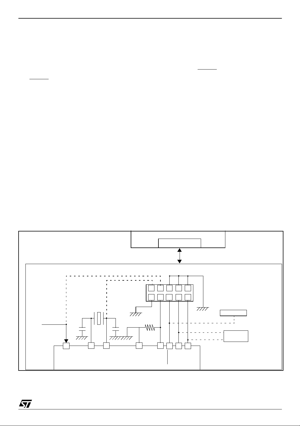
The ST72260G, ST72262G and ST72264G devices are members of the ST7 microcontroller family.
They can be grouped as follows :
– ST72264G devices are designed for mid-range
applications with ADC, I
2
C and SCI interface ca-
pabilities.
– ST72262G devices target the same range of ap-
plications but without I
– ST72260G devices are for applications that do
not need ADC, I
2
C interface or SCI.
2
C peripherals or SCI.
All devices are based on a common industrystandard 8-bit core, featuring an enhanced instruction set.
The ST72F260G, ST72F262G, and ST72F264G
versions feature single-voltage FLASH memory
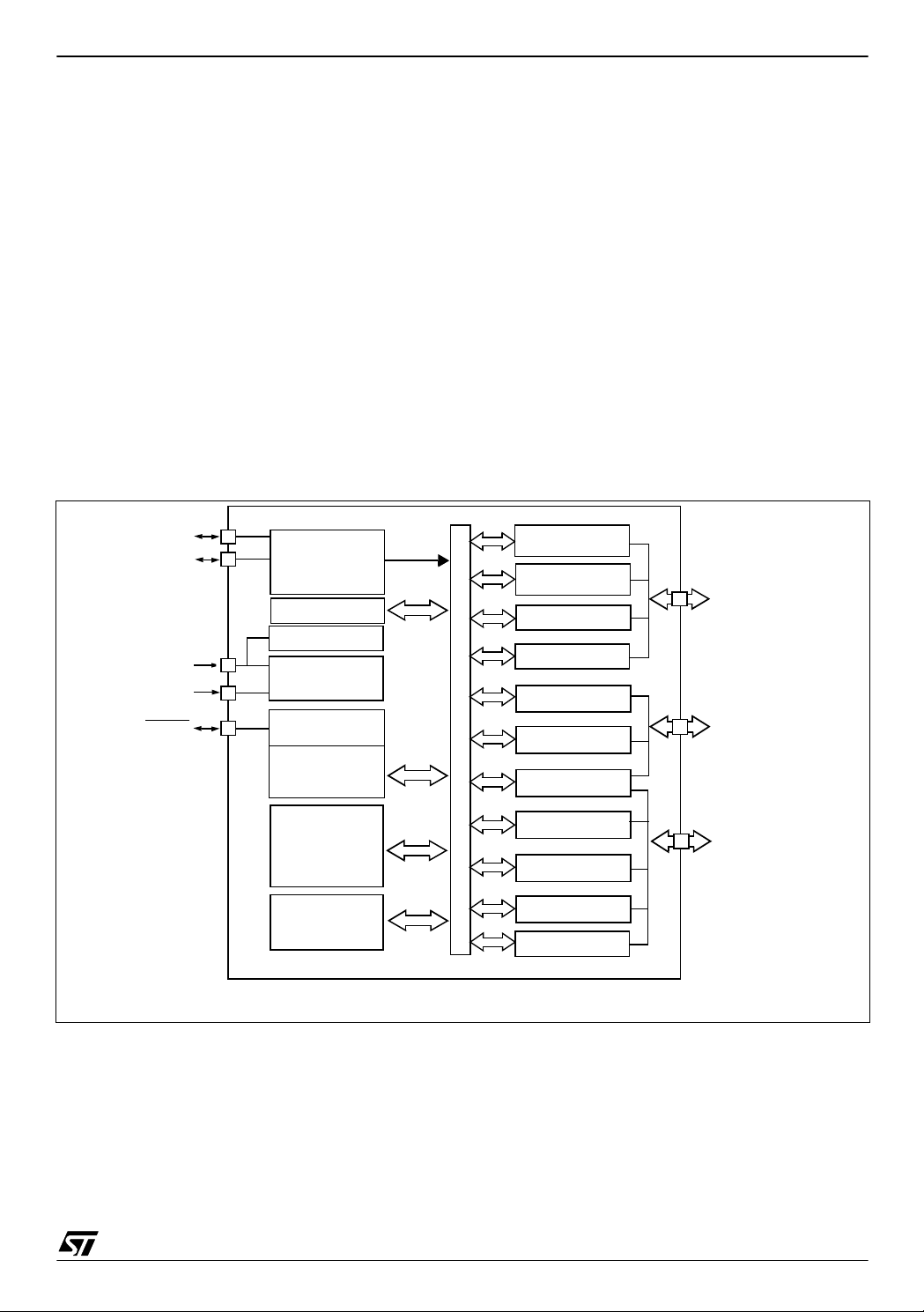
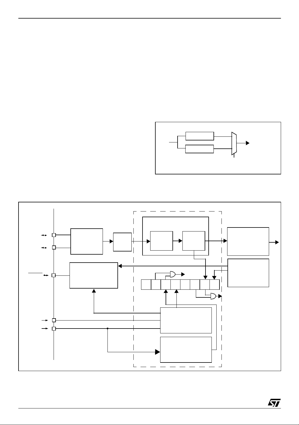
Figure 1. General Block D iagram
Internal
OSC1
OSC2
V
V
RESET
DD
SS
MULTI OSC
+
CLOCK F ILTE R
MCC/RTC
LVD
POWER
SUPPLY
CONTROL
8-BIT CO RE
ALU
CLOCK
with byte-by-byte In-Circuit Programming (ICP)
capabilities.
Under software control, all devices can be placed
in WAIT, SLOW, Ac tive-HALT or H ALT mode, reducing power consumption when the application is
in idle or stand-by state.
The enhanced instruction set and addressing
modes of the ST7 offer both power and flexibility to
software developers, enabling the design of highly
efficient and compact application code. In addition
to standard 8-bit data management, all ST7 microcontrollers feature true bit manipulation, 8x8 unsigned multiplication and indirect addressing
modes.
For easy reference, all parametric data is locat ed
in Section 13 on page 122.
I2C*
SCI*
PA7:0
PORT A
ICD
ADDRESS AND DATA BUS
SPI
PORT B
16-BIT TIMER A
(8 bits)
PB7:0
(8 bits)
PROGRAM
MEMORY
(4 or 8K Bytes)
RAM
(256 Bytes)
*Not avai l abl e on some de vices, see devi ce summar y on page 1.
PORT C
10-BIT ADC*
16-BIT TIMER B
WATCHDOG
PC5:0
(6 bits)
5/171
ST72260G, ST72262G, ST72264G
2 PIN DESCRI PTION
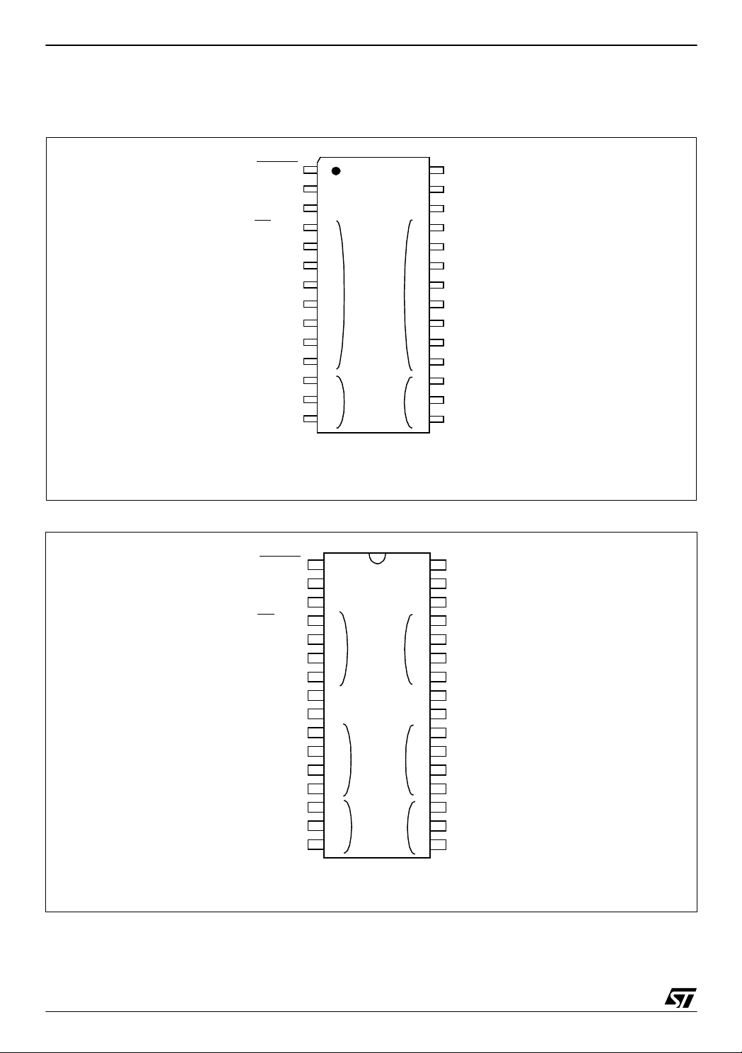
Figure 2. 28-Pin SO Package Pinout
RESET
OSC1
OSC2
SS
/PB7
SCK/PB6
MISO/PB5
MOSI/PB4
OCMP2_A/PB3
ICAP2_A/PB2
OCMP1_A/PB1
ICAP1_A/PB0
AIN5/EXTCLK_A/PC5
2
/OCMP2_B/PC4
AIN4
2
AIN3
/ICAP2_B/PC3
1
Configur abl e by optio n byte
2
Alternate function not available on S T 72260
3
Alternate function not available on S T 72260 and ST72262
Figure 3. 32-Pin SDIP Package Pinout
RESET
OSC1
OSC2
SS
/PB7
SCK/PB6
MISO/PB5
MOSI/PB4
NC
NC
OCMP2_A/PB3
ICAP2_A/PB2
OCMP1_A/PB1
ICAP1_A/PB0
AIN52/EXTCLK_A/PC5
2
/OCMP2_B/PC4
AIN4
2
/ICAP2_B/PC3
AIN3
1
Confi gu rable by option byte
2
Alternate function not available on ST72260
3
Alternate function not available on ST72260 and ST72262
1
2
3
4
5
6
7
8
9
10
11
12
13
14
1
2
3
4
5
6
7
8
9
10
11
12
13
14
15
16
ei1 ei0
ei0 or ei1
ei1
ei0
ei0
ei1
ei0 or ei1
V
28
DD
V
27
SS
ICCSEL
26
(HS)/ICCCLK
PA0
25
(HS)/ICCDATA
PA1
24
PA2
23
22
21
20
19
18
17
1
16
15
32
31
30
29
28
27
26
25
24
23
22
21
20
19
1
18
17
(HS)
PA3 (HS)
PA4 (HS)/SCLI
PA5(HS)/RDI
PA6 (HS)/SDAI
PA7 (HS)/TDO
PC0/ICAP1_B/AIN0
PC1/OCMP1_B/AIN1
PC2/MCO/AIN2
(HS) 20mA high sink capability
eiX associated external interrupt vector
V
DD
V
SS
3
3
3
3
2
2
2
ICCSEL
PA0 (HS)/ICCCLK
PA1 (HS)/ICCDATA
PA2 (HS)
PA3 (HS)
NC
NC
PA4 (HS)/SCLI
PA5 (HS)/RDI
PA6 (HSI/SDAI
PA7 (HS)/TDO
PC0/ICAP1_B/A IN0
PC1/OCMP1_B /AIN1
PC2/MCO/AIN2
(HS) 20mA high sink capability
eiX associated external interrupt vector
3
3
3
3
2
2
2
6/171
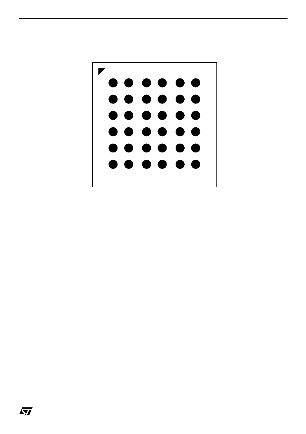
Figure 4. TFBGA Package Pinout (view through package)
123456
A
B
C
D
E
F
ST72260G, ST72262G, ST72264G
7/171
ST72260G, ST72262G, ST72264G
PIN DESCRIPTION (Cont’d)
For external pin connection guidelines, refer to Section 13 "ELECTRICAL CHARACTERISTICS" on page
122.
Legend / Abbreviations for Table 1:
Type: I = input, O = output, S = supply
Input level: A = Dedicated analog input
In/Output lev e l: C
Output level: HS = 20 mA high sink (on N-buffer only)
Port and control configuration:
– Input: float = floating, wpu = weak pull-up, int = interrupt
– Output: OD = open drain
Refer to Section 9 "I/O PORTS" on page 38 for more details on the software configuration of the I/O ports.
The RESET confi g ur at ion of each pin is sho wn in b o ld. This configura ti o n is valid as long as t h e device is
in reset state.
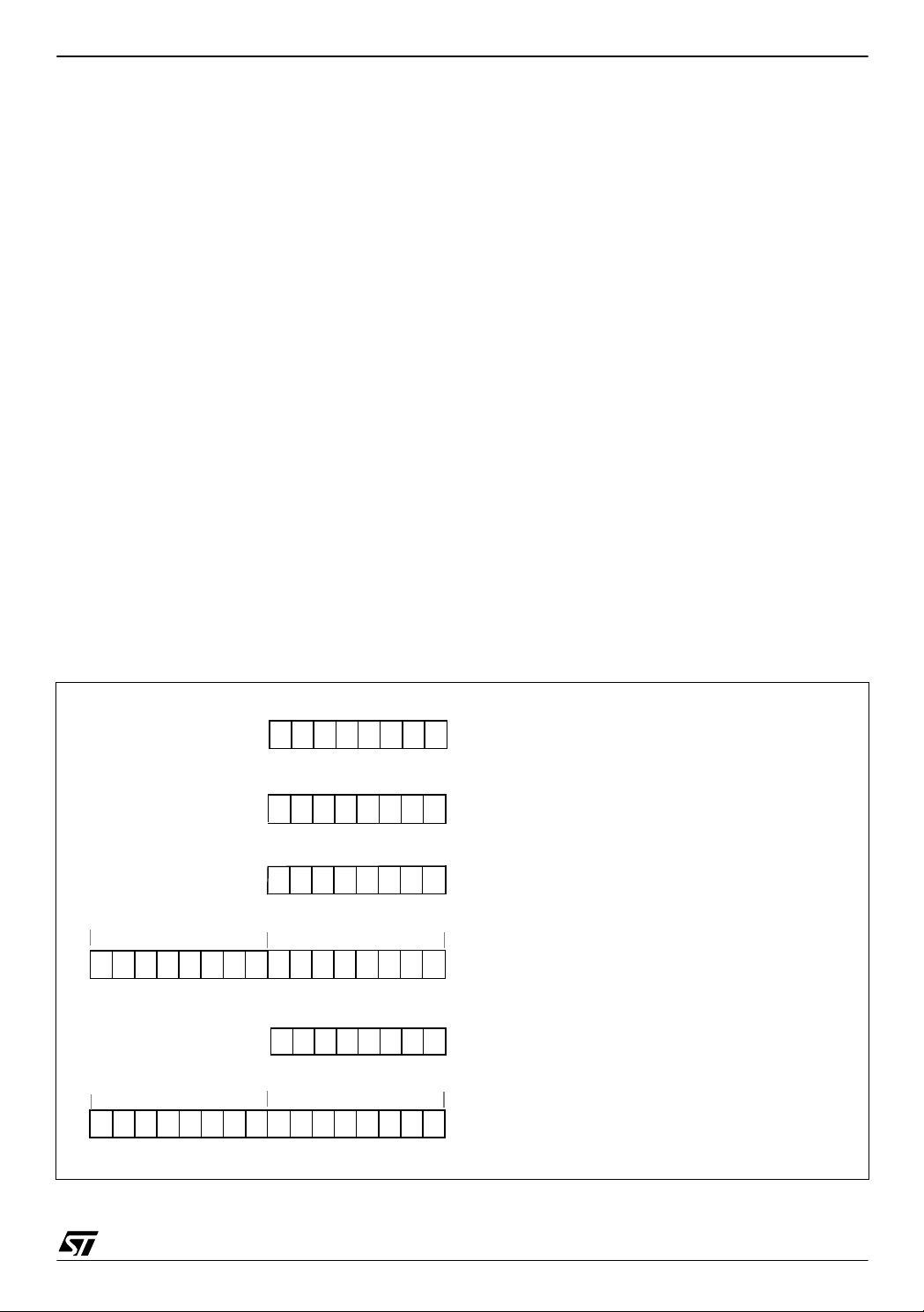
Table 1. Device Pin Description
= CMOS 0.3 VDD/0.7 VDD with input trigger
T
2)
, PP = push-pull
1)
, ana = analog
Pin n°
Level Port / Control
Pin Name
Type
BGA
SO28
SDIP32
1 1 A3 RESET I/O C
2 2 C4 OSC1
3 3 B3 OSC2
4 4 A2 PB7/SS
3)
3)
I/O C
T
I
O
5 5 A1 PB6/SCK I/O C
6 6 B1 PB5/MISO I/O C
7 7 B2 PB4/MOSI I/O C
8 C1 NC
D1 NC
10 8 C3 PB3/OCMP2_A I/O C
11 9 D2 PB2/ICAP2_A I/O C
12 10 E1 PB1 /OCMP1_A I/O C
13 11 F1 PB0 /ICAP1_A I/O C
14 12 F2 PC5/EXTCLK_A/AIN5 I/O C
15 13 E2 PC4/OCMP2_B/AIN4 I/O C
16 14 F3 PC3/ ICAP2_B/AIN3 I/O C
Input
Main
OD
Function
(after
reset)
PP
Alternate Function
Top priority non maskable interrupt (active low)
Input Output
Output
float
wpu
int
XX
ana
External clock input or Resonator oscillator inverter input or resistor input for RC
oscillator
Resonator oscillator inverter output or capacitor input for RC oscillator
X ei1 X X Port B7 SPI Slave Select (active low)
T
X ei1 X X Port B6 SPI Serial Clock
T
X ei1 X X Port B5 SPI Master In/ Slave Out Data
T
X ei1 X X Port B4 SPI Master Out / Slave In Data
T
Not Connected9 C2 NC
X ei1 X X Port B3 Timer A Output Compare 2
T
X ei1 X X Port B2 Timer A Input Capture 2
T
X ei1 X X Port B1 Timer A Output Compare 1
T
X ei1 X X Port B0 Timer A Input Capture 1
T
X ei0/ei1 X X X Port C5
T
X ei0/ei1 X X X Port C4
T
X ei0/ei1 X X X Port C3
T
Timer A Input Clock or ADC
Analog Input 5
Timer B Output Compare 2 or
ADC Analog Input 4
Timer B Input Capture 2 or
ADC Analog Input 3
8/171
ST72260G, ST72262G, ST72264G
Pin n°
SDIP32
SO28
Pin Name
BGA
Level Port / Control
Type
17 15 E3 PC2/MCO/AIN2 I/O C
18 16 F4 PC1/OCMP1_B/AIN1 I/O C
19 17 D3 PC0/ICAP1_B/AIN0 I/O C
20 18 E4 PA7/TDO I/O C
21 19 F5 PA6/SDAI I/O C
22 20 F6 PA5 /RDI I/O C
23 21 E6 PA4/SCLI I/O C
T
T
T
T
24 E5 NC
D5 N C
26 22 C6 PA3 I/O C
27 23 D4 PA2 I/O C
T
T
C5 NC
B6 NC
28 24 A6 PA1/ICCDATA I/O C
29 25 A5 PA0/ICCCLK I/O C
30 26 B5 ICCSEL I C
31 27 A4 V
32 28 B4 V
SS
DD
T
T
T
S Ground
S Main power supply
Main
Input
Input Output
Output
float
X ei0/ei1 X X X Port C2
T
X ei0/ei1 X X X Port C1
T
X ei0/ei1 X X X Port C0
T
wpu
int
ana
OD
Function
(after
reset)
PP
Alternate Function
Main clock output (f
CPU
) or
ADC Analog Input 2
Timer B Output Compare 1 or
ADC Analog Input 1
Timer B Input Capture 1 or
ADC Analog Input 0
HS X ei0 X X Port A7 SCI output
HS X ei0 T Port A6 I2C DATA
HS X ei0 X X Port A5 SCI input
HS X ei0 T Port A4 I2C CLOCK
Not Connected25 D6 NC
HS X ei0 X X Port A3
HS X ei0 X X Port A2
Not Connected
HS X ei0 X X Port A1 In Circuit Communication Data
HS X ei0 X X Port A0
In Circuit Communication
Clock
X ICC mode pin, must be tied low
Notes:
1. In the interrupt input column, “eiX ” define s the asso ciated exte rnal interrupt vec tor. If the weak pul l-up
column (wpu) is merged with the interrupt column (int), then the I/O configuration is a pull-up interrupt input, otherwise the configuration is a floating interrupt input. Port C is mapped to ei0 or ei1 by option byte.
2. In the open drain output column, “T” defines a true open drain I/O (P-Buffer and protection diode to V
are not implemented). See Section 9 "I/O PORTS" on page 38 for more details.
DD
3. OSC1 and OSC2 pins connect a crystal or ceramic resonator, an external RC, or an external source to
the on-chip oscillator see S ection 2 "PIN DESCRIPTION" on page 6 and Section 6.2 "MULTI-OSC ILLA-
TOR (MO)" on page 21 for more details.
9/171
ST72260G, ST72262G, ST72264G
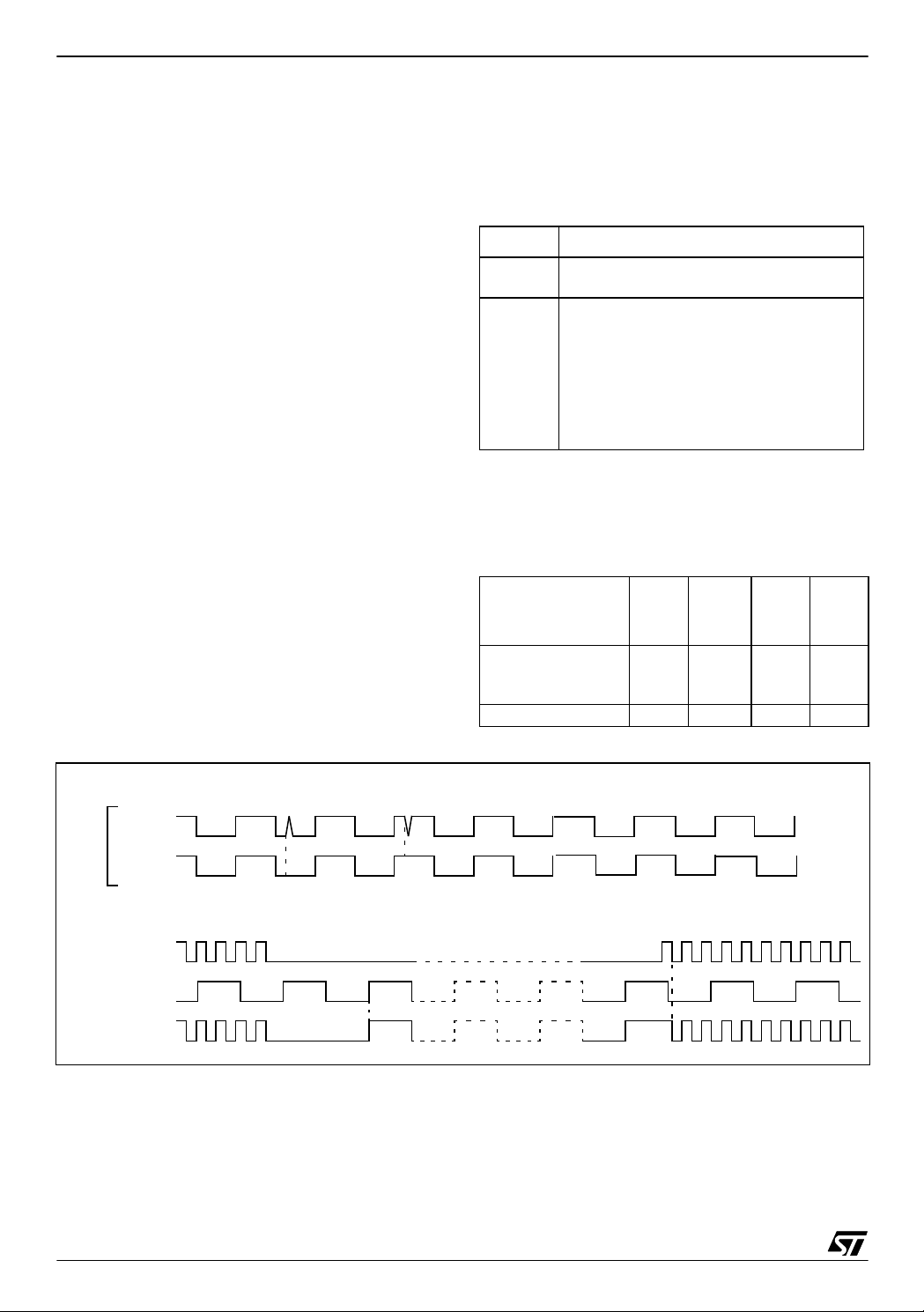
3 REGISTER & MEMORY MAP
As sho wn in Figure 5, the MCU is capable of ad-
dressing 64K bytes of memories and I/O registers.
The available memory locations consist of 128
bytes of register location, 256 bytes of RAM and
up to 8 Kbytes of user program memory. The RAM
space includes up to 128 bytes for the sta ck from
0100h to 017Fh.
The highest address b ytes contain the user reset
and interrupt vectors.
The Flash memory c on tains tw o sectors (s ee Fig-
ure 5) mapped i n the upper part of the ST7 ad-
Figure 5. Me m ory Map
0000h
007Fh
0080h
017Fh
0180h
HW Registers
(see Table 2)
RAM
(256 Bytes)
Reserved
dressing space so the reset and interrupt vectors
are located in Sector 0 (F000h-FFFFh).
The size of Flash Sector 0 and other device options are configurable by Option byte (refer to Sec-
tion 15.1 on page 157).
IMPORTANT: Memory locations marked as “Reserved” must neve r be ac cess ed. A cce ssing a reseved area c an have unpredictable effects on t he
device.
0080h
00FFh
0100h
017Fh
Short Addressing RAM
Zero page
(128 Bytes)
Stack or
16-bit Addressing RAM
(128 Bytes)
8K FLASH
PROGRAM MEMORY
10/171
DFFFh
E000h
FFDFh
FFE0h
FFFFh
Program Memory
(4K, 8 KBytes)
Interrupt & Reset Vectors
(see Table 5 on page 32)
E000h
EFFFh
F000h
FFFFh
4 Kbytes
SECTOR 1
4 Kbytes
SECTOR 0
Table 2. Hardware Register Map
ST72260G, ST72262G, ST72264G
Address Block
0000h
0001h
Port C
0002h
Register
Label
PCDR
PCDDR
PCOR
Register Name
Port C Data Register
Port C Data Direction Register
Port C Option Register
0003h Reserved (1 Byte)
0004h
0005h
0006h
Port B
PBDR
PBDDR
PBOR
Port B Data Register
Port B Data Direction Register
Port B Option Register
0007h Reserved (1 Byte)
0008h
0009h
000Ah
Port A
PADR
PADDR
PAOR
Port A Data Register
Port A Data Direction Register
Port A Option Register
000Bh
to
Reserved (17 Bytes)
001Bh
001Ch
001Dh
001Eh
001Fh
ITC
ISPR0
ISPR1
ISPR2
ISPR3
Interrupt software priority register0
Interrupt software priority register1
Interrupt software priority register2
Interrupt software priority register3
Reset
Status
xx000000h
00h
00h
1)
00h
00h
00h
1)
00h
00h
00h
FFh
FFh
FFh
FFh
1)
Remarks
2)
R/W
2)
R/W
2)
R/W
R/W
R/W
R/W.
R/W
R/W
R/W
R/W
R/W
R/W
R/W
0020h MISCR1 Miscellanous register 1 00h R/W
0021h
0022h
0023h
SPI
SPIDR
SPICR
SPICSR
SPI Data I/O Register
SPI Control Register
SPI Status Register
xxh
0xh
00h
R/W
R/W
R/W
0024h WATCHDOG WDGCR Watchdog Control Register 7Fh R/W
0025h SICSR System Integrity Control / Status Register 000x 000x R/W
0026h MCC MCCSR Main Clock Control / Status Register 00h R/W
0027h Reserved (1 Byte)
2
0028h
0029h
002Ah
002Bh
002Ch
002Dh
002Eh
002Fh
0030h
I2CCR
I2CSR1
2
C
I
I2CSR2
I2CCCR
I2COAR1
I2COAR2
I2CDR
I
C Control Register
2
I
C Status Register 1
2
I
C Status Register 2
2
I
C Clock Control Register
2
I
C Own Address Register 1
2
I
C Own Address Register2
2
I
C Data Register
00h
00h
00h
00h
00h
40h
00h
Reserved (2 Bytes)
R/W
Read Only
Read Only
R/W
R/W
R/W
R/W
11/171

ST72260G, ST72262G, ST72264G
Address Block
0031h
0032h
0033h
0034h
0035h
0036h
0037h
0038h
TIMER A
0039h
003Ah
003Bh
003Ch
003Dh
003Eh
003Fh
Register
Label
TACR2
TACR1
TASCSR
TAIC1HR
TAIC1LR
TAOC1HR
TAOC1LR
TACHR
TACLR
TAACHR
TAACLR
TAIC2HR
TAIC2LR
TAOC2HR
TAOC2LR
Register Name
Timer A Control Register 2
Timer A Control Register 1
Timer A Control/Status Register
Timer A Input Capture 1 High Register
Timer A Input Capture 1 Low Register
Timer A Output Compare 1 High Register
Timer A Output Compare 1 Low Register
Timer A Counter High Register
Timer A Counter Low Register
Timer A Alternate Counter High Register
Timer A Alternate Counter Low Register
Timer A Input Capture 2 High Register
Timer A Input Capture 2 Low Register
Timer A Output Compare 2 High Register
Timer A Output Compare 2 Low Register
Reset
Status
00h
00h
xxh
xxh
xxh
80h
00h
FFh
FCh
FFh
FCh
xxh
xxh
80h
00h
0040h MISCR2 Miscellanous register 2 00h R/W
0041h
0042h
0043h
0044h
0045h
0046h
0047h
0048h
0049h
004Ah
004Bh
004Ch
004Dh
004Eh
004Fh
TIMER B
TBCR2
TBCR1
TBSCSR
TBIC1HR
TBIC1LR
TBOC1HR
TBOC1LR
TBCHR
TBCLR
TBACHR
TBACLR
TBIC2HR
TBIC2LR
TBOC2HR
TBOC2LR
Timer B Control Register 2
Timer B Control Register 1
Timer B Control/Status Register
Timer B Input Capture 1 High Register
Timer B Input Capture 1 Low Register
Timer B Output Compare 1 High Register
Timer B Output Compare 1 Low Register
Timer B Counter High Register
Timer B Counter Low Register
Timer B Alternate Counter High Register
Timer B Alternate Counter Low Register
Timer B Input Capture 2 High Register
Timer B Input Capture 2 Low Register
Timer B Output Compare 2 High Register
Timer B Output Compare 2 Low Register
00h
00h
xxh
xxh
xxh
80h
00h
FFh
FCh
FFh
FCh
xxh
xxh
80h
00h
Remarks
R/W
R/W
R/W
Read Only
Read Only
R/W
R/W
Read Only
Read Only
Read Only
Read Only
Read Only
Read Only
R/W
R/W
R/W
R/W
R/W
Read Only
Read Only
R/W
R/W
Read Only
Read Only
Read Only
Read Only
Read Only
Read Only
R/W
R/W
0050h
0051h
0052h
0053h
0054h
0055h
0056h
SCI
SCISR
SCIDR
SCIBRR
SCICR1
SCICR2
SCIERPR
SCIETPR
SCI Status Register
SCI Data Register
SCI Baud Rate Register
SCI Control Register1
SCI Control Register2
SCI Extended Receive Prescaler Register
SCI Extended Transmit Prescaler Register
C0h
xxh
00h
x000 0000h
00h
00h
00h
Read Only
R/W
R/W
R/W
R/W
R/W
R/W
0057h
to
Reserved (24 Bytes)
006Eh
006Fh
0070h
0071h
ADC
ADCDRL
ADCDRH
ADCCSR
Data Register Low
Data Register High
Control/Status Register
3)
3)
00h
00h
00h
Read Only
Read Only
R/W
0072h FLASH FCSR F lash Contr ol Register 00h R/W
0073h
to
Reserved (13 Bytes)
007Fh
12/171

ST72260G, ST72262G, ST72264G
Legend: x=Unde fined, R/W=R e ad/Write
Notes:
1. The contents of the I/O p ort DR registers are readable only i n out put c onf iguration. I n i nput c onf iguration, the values of the I/O pins are returned instead of the DR register contents.
2. The bits associated with unavailable pins must always keep their reset value.
3. For compatibility with the ST72C254, the ADCDRL and ADCDRH data registers are located with the
LSB on the lower address (6Fh) and the MSB on the higher address (70h). As this scheme is not little Endian, the ADC data registers cannot be treated by C programs as an integer, but have to be treated as two
char registers.
13/171

ST72260G, ST72262G, ST72264G
4 FLASH PROGRAM MEMO RY
4.1 In troduction
The ST7 single voltage extended Flash (XFlash) is
a non-volatile memory that can be electrically
erased and programmed either on a by te-by-byte
basis or up to 32 bytes in parallel.
The XFlash devices can be programmed off-board
(plugged in a programming tool) or on-board using
In-Circuit Programming or In-Application Programming.
The array matrix organ isation allows each sector
to be erased and reprogrammed wi thout affecting
other sectors.
4.2 Main Features
■ ICP (In-Circuit Programming)
■ IAP (In-Application Programming)
■ ICT (In-Circuit Testing) for downloading and
executing user application test patterns in RAM
■ Sector 0 size configurable by option byte
■ Read-out and write protection against piracy
4.3 PROGRAMMING MODES
The ST7 can be programmed in three different
ways:
– Insertion in a programming tool. In this mode,
FLASH sectors 0 and 1 and op tion byte row
can be programmed or erased.
– In-Circuit Programming. In this mode, FLAS H
sectors 0 and 1 and op tion byte row can be
programmed or erased without removing the
device from the application board.
– In-Application Programming. In this mode,
sector 1 can be programme d or erased without removing the device from the application
board and while the application is running.
4.3.1 In-Circuit Programming (ICP)
ICP us es a pr ot o c ol c al l e d I CC ( I n- Ci r c ui t C om mu nication) which allows an ST7 plugged on a printed circuit board (PCB) to communicate with an external programming device connected via cable.
ICP is performed in three steps:
Switch the ST7 to ICC mode (In-Circuit Communications). This is done by driving a specific signal
sequence on the ICCCLK/DATA pins while the
RESET pin is pulled low. When the ST7 enters
ICC mode, it fetches a specific RESET vector
which points to the ST7 System Memory containing the ICC protocol routine. This routine enables
the ST7 to receive bytes from the ICC interface.
– Download ICP Driver cod e in RAM from the
ICCDATA pin
– Execute ICP Driver code in RAM to program
the FLASH memory
Depending on the ICP Driver code downloaded in
RAM, FLASH memo ry programming can be fully
customized (number of bytes to program, program
locations, or selection of the serial communication
interface for downloading).
4.3.2 In Application Programming (IAP)
This mode uses an IAP Driver program previously
programmed in Sector 0 by the user (in ICP
mode).
This mode is fully controlled by user software. This
allows it to be adapted to the user application, (user-defined strategy for entering programming
mode, choice of c om mun ications protoc ol used t o
fetch the data to be stored etc.)
IAP mode can be used to program any memory areas except Sector 0, which is write/erase protected to allow recovery in case errors occur during
the programming operation.
14/171
FLASH PROGRAM MEMORY (Cont’d)
ST72260G, ST72262G, ST72264G
4.4 ICC interface
ICP needs a minimum of 4 and u p to 7 pins to be
connected to the programming tool. These pins
are:
– RESET
–V
: device reset
: device power supply ground
SS
– ICCCLK: ICC output serial clock pin
– ICCDATA: ICC input serial data pin
– ICCSEL: ICC selection (not required on devic-
es without ICCSEL pin)
– OSC1: main clock input for external source
(not required on devices without OSC1/OSC2
pins)
: application board power supply (option-
–V
DD
al, see Note 3)
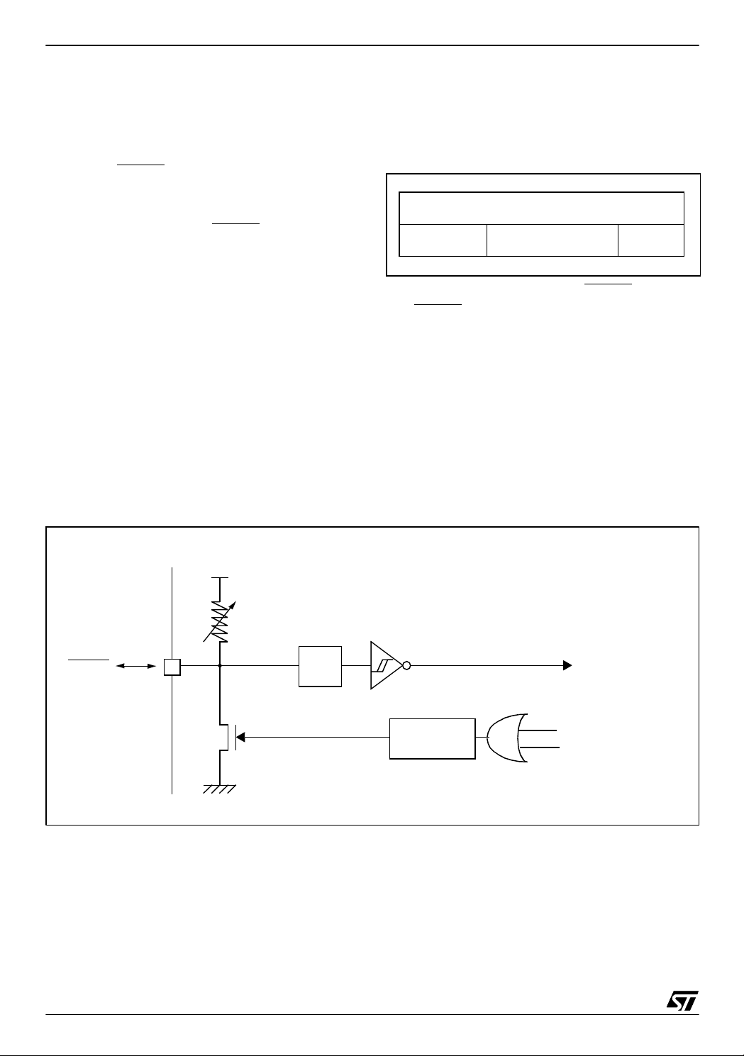
Notes:
1. If the ICCCLK or ICCDATA pins are only use d
as outputs in the application, no sign al iso lation is
necessary. As soon as the Programming Tool is
plugged to the board, even if an ICC session is not
in progress, the ICCCLK and ICCDATA pins are
not available for the application. If they are used as
inputs by the application, isolation such as a serial
resistor has to be implemented in case another device forces the signal. Refer to the Programming
Figure 6. Typical ICC Interface
Tool documentation for recommended resistor values.
2. During the ICP session, the programming tool
must contr o l the RESET
pin. This can lead to conflicts between the programming tool and the application reset circuit if it drives more than 5mA at
high level (push pull output or pull-up resistor<1K).
A schottky diode can be u sed to isolate t he application RESET circuit in this case. When using a
classical RC network with R>1K or a reset management IC with open drain outpu t and pull-up resistor>1K, no additional com ponents are needed.
In all cases the user must ensure that no external
reset is generated by the application during the
ICC session.
3. The use of Pin 7 of the ICC connec tor depends
on the Programming Tool architecture. This pin
must be connected when using most ST Programming Tools (it is used to monitor the application
power supply). Please refer to the Programming
Tool manual.
4. Pin 9 has to be connected to the OSC1 pin of
the ST7 when the clock is not avai lable in the application or if the selected clock option is not programmed in the option byte. ST7 devices with multi-oscillator capability need to have OSC2 grounded in this case.
APPLICATION
POWER SUPPLY
OPTIONAL
(See Note 3)
C
L2
VDD
OSC2
OPTIONAL
(See Note 4)
C
L1
OSC1
ST7
PROGRAMMING TOOL
ICC CONNECTOR
ICC Ca ble
ICC CONNECTOR
HE10 CONNECTOR TYPE
975 3
10kΩ
VSS
RESET
ICCSEL
ICCCLK
1
246810
ICCDATA
APPL ICATION BOARD
APPLICATION
RESET SOURCE
See Note 2
See Note 1
APPLICATION
I/O
15/171

ST72260G, ST72262G, ST72264G
FLASH PROGRAM MEMORY (Cont’d)
4.5 Memory Protection
There are two different types of memory protection: Read Out Protection and Write/Erase Protection which can be applied individually.
4.5.1 Read out Protection
Read out protection, when selected, makes it impossible to extract the m emory content from the
microcontroller, thus preventing piracy.
In flash devices, this protection is removed by reprogramming the option. In this case the program
memory is automatically erased and the device
can be reprogrammed.
Read-out protection selection depends on the device type:
– In Flash devices it is enabled and removed
through the FMP_R bit in the option byte.
– In ROM devices it is enabled by mask option
specified in the Option List.
4.5.2 Flash Write/Erase Protection
Write/erase protection, when set, makes it impossible to both overwrite and erase program memory. Its purpose is to provide advanced security to
applications and prevent a ny change bei ng mad e
to the memory content.
Warning: Once set, Write/erase protection can
never be removed. A write-protected flash device
is no longer reprogrammable.
Write/erase protection is enabled through the
FMP_W bit in the option byte.
4.6 Register Description FLASH CONTROL/STATUS REGISTER (FCSR)
Read/Write
Reset Value: 000 0000 (00h)
1st RASS Key: 0101 0110 (56h)
2nd RASS Key: 1010 1110 (AEh)
70
00000OPTLATPGM
Note: This register is reserved for programming
using ICP, IAP or other program ming methods. It
controls the XFlash p ro grammin g and erasing operations. For details on XFlash programming, refer
to the ST7 Flash Programming Reference Manual.
When an EPB or another programming tool is
used (in socket or ICP mode), the RASS k eys are
sent automatically.
16/171
5 CENTRAL PRO CESSING UNIT
ST72260G, ST72262G, ST72264G
5.1 INTRODUCTION
This CPU has a full 8-bit architecture and contains
six internal registers allowing efficient 8-bit data
manipulation.
5.2 MAIN FEATURES
■ Enable executing 63 basic instructions
■ Fast 8-bit by 8-bit multiply
■ 17 main addressing modes (with indirect
addressing mode)
■ Two 8-bit index registers
■ 16-bit stack pointer
■ Low power HALT and WAIT modes
■ Priority maskable hardware interrupts
■ Non-maskable software/hardware interrupts
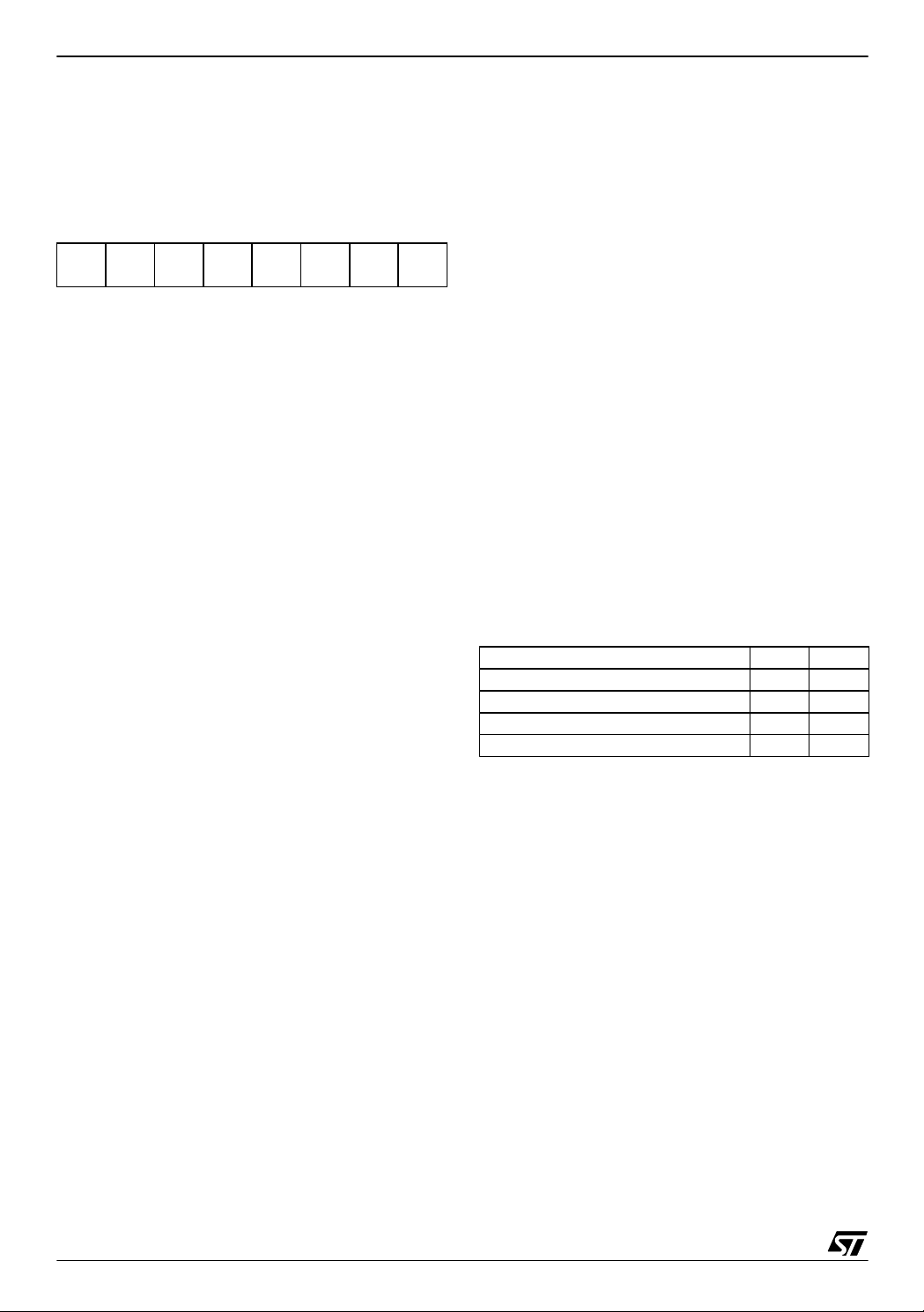
Figure 7. CPU Registers
5.3 CPU REGISTERS
The 6 CPU registers shown in Figure 7 are not
present in the memory mapping and are accessed
by specifi c ins t r uc tions.
Accumulator (A)
The Accumulator is an 8-bit general purpose register used to hold operan ds and the results of the
arithmetic and logic calculations and to manipulate
data.
Index Registers (X and Y)
These 8-bit registers are used to create effective
addresses or as tempora ry storage areas f or dat a
manipulation. (The Cross-A ssembler generates a
precede instruction (PRE) to indicate that the following instruction refers to the Y register.)
The Y register is not affected by the interrupt automatic procedures.
Program Cou nt er (P C )
The program counter is a 16-bit register containing
the address of the next instruction to be executed
by the CPU. It is made of two 8-bit registers PCL
(Program Counter Low which is the LSB) and PCH
(Program Counter High which is the MSB).
70
RESET VALUE = XXh
70
RESET VALUE = XXh
70
RESET VALUE = XXh
15 8
RESET VALUE = RESET VECTOR @ FFFEh-FFFFh
15
RESET VALUE = STACK HIGHER ADDRESS
PCH
RESET VALUE =
7
70
1C1I1HI0NZ
1X11X1XX
70
8
PCL
0
ACCUMULA T OR
X INDEX REGISTER
Y INDEX REGISTER
PROGRAM COUNTER
CONDITION CODE REGISTER
STACK POINTER
X = Undefined Value
17/171
ST72260G, ST72262G, ST72264G
CENTRAL PROCESSING UNIT (Cont’d)
Condition Code Register (CC)
Read/Write
Reset Value: 111x1xxx
70
11I1HI0NZ
C
The 8-bit Condition Code register c ontains the interrupt masks and four flags representative of the
result of the instruction just executed. This register
can also be handled by the PUSH and POP instructions.
These bits can be individually tested and/or controlled by specific instructions.
Arithmetic Management Bits
Bit 4 = H
Half carry
.
This bit is set by hardware when a carry occurs between bits 3 and 4 of t he ALU during an ADD or
ADC instructions. It is reset by hardware during
the same instruction s.
0: No half carry has occurred.
1: A half carry has occurred.
This bit is tested using the JRH or JRNH instruction. The H bit is useful in BCD arithmetic subroutines .
Bit 2 = N
Negative
.
This bit is set and cleared by hardware. It is representative of the result sign of the last arithmetic,
logical or data manipulation. I t’s a copy of the re-
th
sult 7
bit.
0: The result of the last operation is positive or null.
1: The result of the last operation is negative
(i.e. the most significant bit is a logic 1).
This bit is accessed by the JRMI and JRPL instructions.
Bit 1 = Z
Zero
.
This bit is set and cleared by hardware. This bit indicates that the result of the last arithmetic, logical
or data manipulation is zero.
0: The result of the last operation is different from
zero.
1: The result of the last operation is zero.
This bit is accessed by the JREQ and JRNE test
instructions.
Bit 0 = C
Carry/borrow.
This bit is set and cleared b y hardware and software. It indicates an overflow or an underflow has
occurred during the last arithmetic operation.
0: No overflow or underflow has occurred.
1: An overflow or underflow has occurred.
This bit is driven by the SCF and RCF instructions
and tested by the JRC and JRNC instructions. It is
also affected by the “bit test and branch”, shift and
rotate instructions.
Interrupt Managem ent B i ts
Bit 5,3 = I1, I0
Interrupt
The combination of the I1 and I0 bits gives the current interrupt software priority.
Interrupt Software Priorit y I1 I0
Level 0 (main) 1 0
Level 1 0 1
Level 2 0 0
Level 3 (= interrupt disable) 1 1
These two bits are set/cleared b y hardware when
entering in interrupt. The loaded value is given by
the corresponding bits in the interrupt software priority registers (IxSPR). They can be also set/
cleared by software with the RIM, SIM, IRET,
HALT, WFI and PUSH/POP instructions.
See the interrupt management chapter for more
details.
18/171
CENTRAL PROCESSING UNIT (Cont’d)
ST72260G, ST72262G, ST72264G
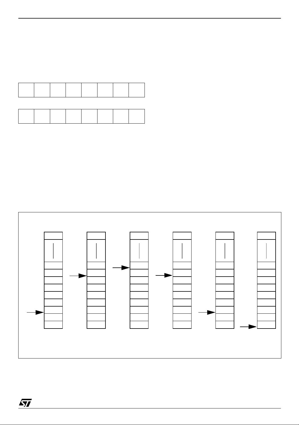
Stack Pointer (SP)
Read/Write
Reset Value: 01 7Fh
15 8
00000001
The least significant byte of the Stack Pointer
(called S) can be directly accessed by a LD instruction.
Note: When the lower limit is exceeded, the Stack
Pointer wraps around to the stack upper limit, wi thout indicating the s tack overflow. The previously
stored information is then o verwritten and therefore lost. The stack also wraps in case of an underflow.
70
SP7 SP6 SP5 SP4 SP3 SP2 SP1
SP0
The stack is used to save the retu rn address during a subroutine call and the CPU context during
an interrupt. The user may also directly manipulate
the stack by means of the PUSH and POP instruc-
The Stack Pointer is a 16-bit register which is always pointing to the next free location in the stack.
It is then decremented after data has been pushed
onto the stack and incremented before data is
popped from the stack (see Figure 8).
Since the stack is 128 bytes deep, the 8 most significant bits are forced by hardw are. Following a n
MCU Reset, or after a Reset Stack Pointe r instruction (RSP), the Stack Pointer contains its reset value (the SP7 to SP0 bits are set) which is the stack
tions. In the case of an interrupt, the PCL is stored
at the first location point ed to by the SP. Then the
other registers are stored in the next locations as
shown in Figure 8
– When an interrupt is received, the SP is decre-
mented and the context is pushed on the stack.
– On return from interrupt, the SP is incremented
and the context is popped from the stack.
A subroutine call occupies two locations and an interrupt five locat ions i n the sta ck ar ea.
higher address.
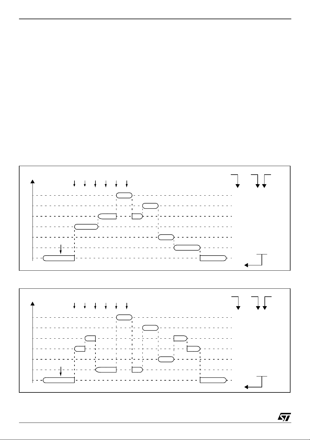
Figure 8. Stack Manipulation Example
CALL
Subroutine
Interrupt
Event
PUSH Y POP Y IRET
RET
or RSP
@ 0100h
SP
@ 017Fh
SP
CC
A
X
PCH
PCL
PCH
PCL
Stack Higher Address = 017Fh
Stack Lower Address =
PCH
PCL
0100h
SP
Y
CC
A
X
PCH
PCL
PCH
PCL
SP
CC
A
X
PCH
PCL
PCH
PCL
SP
PCH
PCL
SP
19/171
ST72260G, ST72262G, ST72264G
6 SUPPLY, RESET AND CLOCK M ANAGEMENT
The device includes a range of utility features for
securing the application in critical situations (for
example in case of a power brown-out), and reducing the number of external components. An
overview is shown in Figure 10.
For more details, refer to dedicated parametric
section.
Main Features
■ Optional PLL for multiplying th e frequency by 2
(not to be used with internal RC oscillator)
■ Reset Sequence Manager (RSM)
■ Multi-Oscillator Clock Management (MO)
– 4 Crystal/ C e ra m ic res on ator oscilla t or s
– 1 Internal R C os c illa t or
■ System Integrity Management (SI)
– Main supply Low Voltage Detector (LVD)
– Auxiliary Voltage Detector (AVD) with inter-
rupt capability for monitori ng the main s upply
– Clock Security System (CSS) wi th Clo ck Filter
and Backup Safe Oscillator (enabled by option byte)
Figure 10. Clock, Reset and Supply Block Diagram
SYSTEM INTEGRITYMANAGEMENT
6.1 PHASE LOCKED LOOP
If the clock frequency input to the PLL is in the 2 to
4 MHz range, the P LL can be used to mu ltiply the
frequency by two to obtain an f
of 4 to 8 MHz.
OSC2
The PLL is enable d by option byte. If the PLL is
disabled, then f
OSC2 = fOSC
/2.
Caution: T he PLL is not recom mended for applications where timing accuracy is required. See
“PLL Characteristics” on page 134.
Figure 9. PLL Block Diagram
f
OSC
PLL x 2
/ 2
0
1
PLL OPTION BIT
f
OSC2
OSC2
OSC1
RESET
V
SS
V
DD
MULTI-
OSCILLATOR
(MO)
RESET SEQUENCE
MANAGER
(RSM)
f
OSC
PLL
(option)
f
OSC2
CLOCK SECURITYSYSTEM
CLOCK
FILTER
SICSR
AVD AVD
0
(CSS)
AVD Interrupt Requ est
LVD
F
RF
LOW VOLTAGE
DETECTOR
(LVD)
AUXILIARY VOLTAGE
DETECTOR
(AVD)
f
SAFE
OSC
CSS
0
IEIE
CSS Interrupt Request
OSC2
CSSDWDG
RF
MAIN CLOCK
CONTRO LLER
WITH REALTIME
CLOCK ( MCC/RTC)
WATCHDOG
TIMER (WDG )
f
CPU
20/171
6.2 MULTI-OSCILLATOR (MO)
ST72260G, ST72262G, ST72264G
The main clock of the ST7 can be generated by
four different source types coming from the multioscillator block:
■ an external source
■ 5 crystal or ceramic resonator oscillators
■ an internal high frequency RC oscillator
Each oscillator is optimized for a given frequenc y
range in terms of consumption and is selectable
through the option byte. The associated hardware
configurations are shown in Table 3. Refer to the
electrical characteristics section for more details.
Caution: The OS C1 and/or OSC2 pins must not
be left unconnected. For th e purposes of Failure
Mode and Effects Analysis, it should be noted that
if the OSC1 and/or OSC2 pin s are left unconnec ted, the ST7 main oscillat or may start and, in this
configuration, could generate an f
clock fre-
OSC
quency in excess of the allowed maximum
(>16MHz.), putting the ST7 in an unsafe/undefined state. The product behaviour must therefore
be considered undefined when the OSC pins are
left unconnected.
External Clock Source
In this external clock mode, a clock signal (square,
sinus or triangle) with ~50% duty cycle has to drive
the OSC1 pin while the OSC2 pin is tied to ground.
Crystal/Ceramic Oscillators
This family of oscillators has the advantage of producing a very accurate rate on the main clock of
the ST7. The select ion within a list of 5 oscillators
with different frequency ranges has to be done by
option byte in order to reduce c onsumption (refer
to Se ction 15.1 on page 157 for more details o n
the frequency ranges). In this mode of the m ultioscillator, the resonator and the load capacitors
have to be placed as close as possible to the oscillator pins in order to minimize output distortion and
start-up stabilization time. The loading capacitance values must be adjusted according to the
selected oscilla tor .
These oscillators are not stopped during the
RESET phase to avoid losing time in the oscillator
start-up phase.
Internal RC Oscillator
This oscillator allows a low cost solution for the
main clock of the ST7 using only an internal resistor and capacit or. Int er nal R C os cillator mode has
the drawback of a lower frequency accuracy and
should not be used in applications that require accurate timing .
In this mode, the two oscillator pins have to be tied
to ground.
Table 3. ST7 Clock Sources
Hardware Configur ation
ST7
OSC1 OSC2
External ClockCrystal/Cera mic ResonatorsInternal RC Oscillator
EXTERNAL
SOURCE
OSC1 O SC2
C
L1
CAPACITORS
OSC1 OSC2
ST7
LOAD
ST7
C
L2
21/171
ST72260G, ST72262G, ST72264G
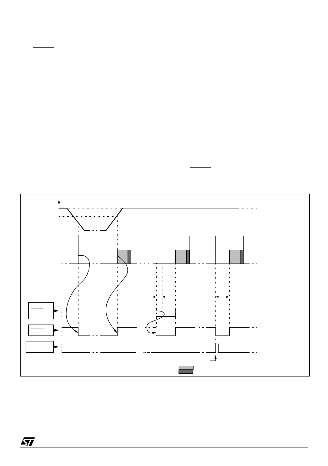
6.3 RESET SEQUENCE MANAGER (RSM)
6.3.1 Introd uct i on
The reset sequence manager in cludes three RESET sources as shown in Figure 12:
■ External RESET source pulse
■ Internal LVD RESET (Low Voltage Detection)
■ Internal WATCHDOG RESET
These sources act on the RESET
pin and it is al-
ways kept low during the delay phase.
The RESET service routine vector is fixed at ad-
dresses FFFEh-FFFFh in the ST7 memory map.
The basic RESET s eque nc e cons i sts o f 3 p has es
as shown in F igure 11:
■ Active Phase depending on the RESET source
■ 4096 CPU clock cycle delay (selected by option
byte)
■ RESET vector fetch
The 4096 CPU clock cycle delay allows the oscillator to stabilise and ensures that recovery has
taken place from the Reset state. The shorter or
longer clock cycle delay should be selected by option byte to correspond to the stabiliza tion time of
the external oscillator used in the appl icat ion.
Figure 12. Reset Block Diagram
The RESET vector fetch phase duration is 2 clock
cycles.
Figure 11. RESET Sequence Phases
RESET
Active Phase
INTERNAL RESET
4096 CLOCK CYCLES
6.3.2 Async hronous External R ESET
The RESET
output with integrated R
pin is both an input and an open-drain
weak pull-up resistor.
ON
FETCH
VECTOR
pin
This pull-up has no f ixed value but varies in accordance with the input voltage. It
can be pulled
low by external circuitry to reset the device. See
Electrical Characteristic section for more details.
A RESET signal originating from an external
source must have a duration of at least t
h(RSTL)in
in
order to be recognized (see Figure 13). This detection is asynchronous and therefore the MCU
can enter reset state even in HALT mode.
RESET
V
DD
R
ON
Filter
PULSE
GENERATOR
INTERNAL
RESET
WATCHDOG RESE T
LVD RESET
22/171
RESET SEQUENCE MANAGER (Cont’d)
The RESET
pin is an asynchronous signal which
plays a major role in EMS performance. In a noisy
environment, it is recommended to follow the
guidelines mentioned in the electr ical characteristics section.
6.3.3 External Power-On RESET
If the LVD is disabled by option byte, to start up t he
microcontroller correctly, the user must ensure by
means of an external reset circuit that the reset
signal is held low until V
level specified for the selected f
A proper reset signal for a slow rising V
is over the m inimum
DD
frequency.
OSC
supply
DD
can generally be provide d by an ex ternal RC network connected to the RESET
pin.
Figure 13. RESET Sequences
V
DD
ST72260G, ST72262G, ST72264G
6.3.4 Internal Low Voltage Detector (LVD) RESET
Two differen t RESET sequences caused by the internal LVD circuitry can be distinguished:
■ Power-On RESET
■ Voltage Drop RESET
The device RESET
pulled low when V
V
DD<VIT-
(falling edge) as shown in Figure 13.
The LVD filters spikes on V
avoid parasitic resets.
6.3.5 Internal Watchdog RESET
The RESET sequence generated by a internal
Watchdog counter overflow is shown in Figure 13.
Starting from the Watchdog counter underflow, the
device RESET
low during at least t
pin acts as an output that is
DD<VIT+
(rising edge) or
larger than t
DD
g(VDD)
pin acts as an output that is pulled
w(RSTL)out
.
to
V
IT+(LVD)
V
IT-(LVD)
EXTERNAL
RESET
SOURCE
RESET PIN
WATCHDOG
RESET
RUN
LVD
RESET
ACTIVE PHASE
RUN
t
h(RSTL)in
EXTERNAL
RESET
ACTIVE
PHASE
WATCHDOG UNDERFLOW
RUN RUN
INTERNAL RESET (4096 T
VECTOR FETCH
WATCHDO G
RESET
ACTIVE
PHASE
t
w(RSTL)out
CPU
)
23/171
ST72260G, ST72262G, ST72264G
6.4 SYSTEM INTEGRITY MANAGEMENT (SI)
The System Integrity Managem ent block contains
group the Low voltage Detector (LVD), Auxiliary
Voltage Detector (AVD) and Clock Security System (CSS) functions. It is managed by the SICSR
register.
6.4.1 Low Voltage Detector (LVD)
The Low Voltage Detector funct ion (LVD) generates a static reset when the V
below a V
reference value. This means that it
IT-
supply voltage is
DD
secures the power-up as well as the power-down
keeping the ST7 in reset.
The V
than the V
reference value for a voltage drop is lower
IT-
reference value for power-on in order
IT+
to avoid a parasitic reset when the MCU starts running and sinks current on the supply (hysteresis).
The LVD Reset circuitry generates a reset when
is below:
V
DD
when VDD is rising
–V
IT+
–V
when VDD is falling
IT-
The LVD func t ion is illustrated in F igure 14.
Figure 14. Low Voltage Detector vs Reset
V
DD
The voltage threshold can be configured by option
byte to be low, medium or high.
Provided the minimum V
the oscillator frequency) is above V
value (guaranteed for
DD
, the MCU
IT-
can only be in two modes:
– under full software control
– in static safe reset
In these conditions, secure operation is always ensured for the application without the need for external reset hardware.
During a Low Voltage Detector Reset, the RESET
pin is held low, thus p ermitting the MCU to reset
other devices.
Notes:
The LVD allows the device to be used without any
external RESET circuitry.
The LVD is an optional function whi ch can be se-
lected by option byte.
V
V
RESET
IT+
IT-
V
hys
24/171
SYSTEM INTEGRITY MANAGEMENT (Cont’d)
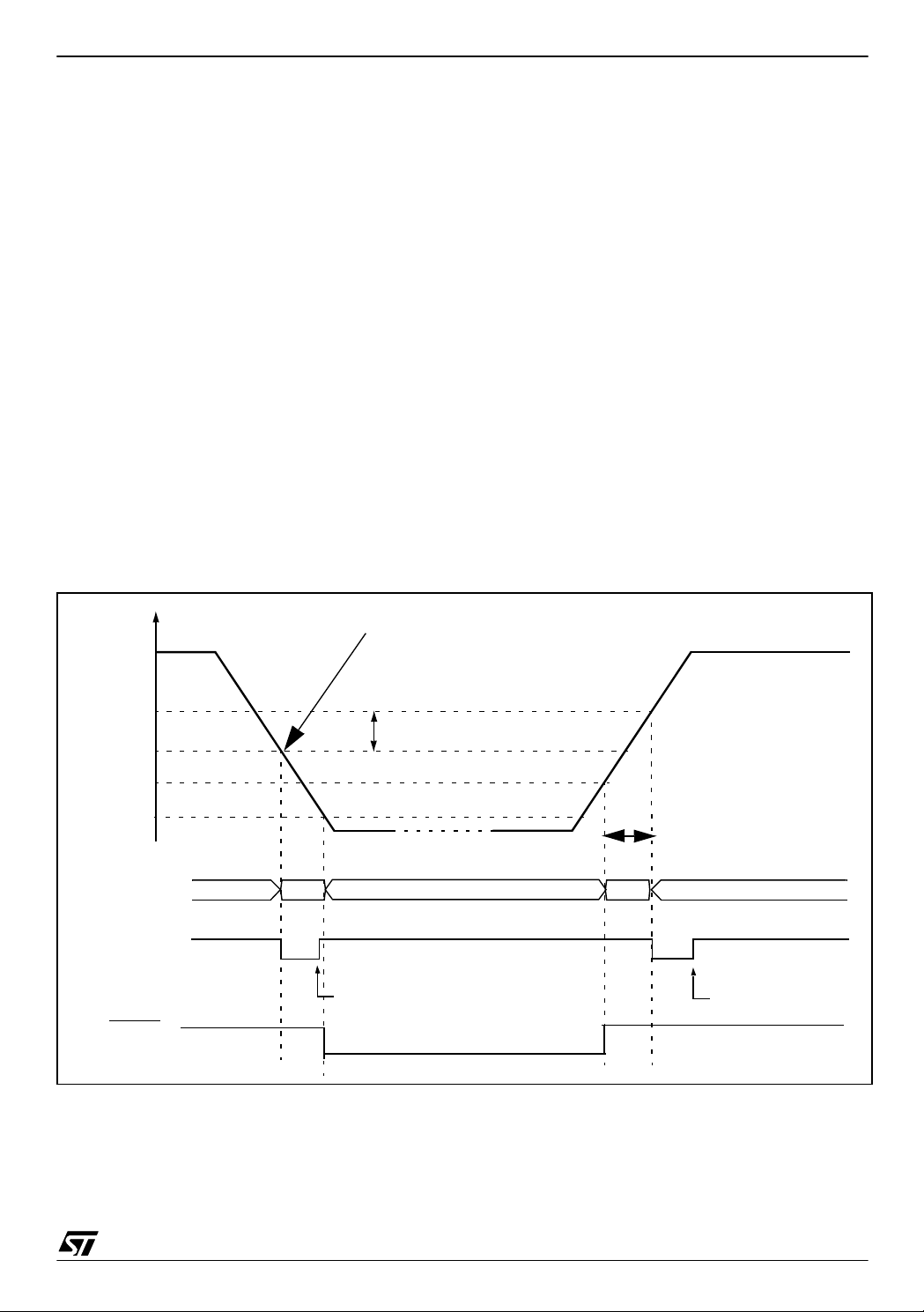
6.4.2 Auxiliary Voltage Detector (AVD)
The Voltage Detector function (AVD) is based on
an analog comparison between a V
erence value and the V
main supply. The V
DD
and V
IT-
IT+
ref-
IT-
reference value for falling voltage is lower than the
V
reference value for rising voltage in order to
IT+
avoid parasitic detection (hysteresis).
The output of the AVD comparator is directly read-
able by the application software through a real
time status bit (VDF) in the SICSR register. This bit
is read only.
Caution: The AVD functions only if the LVD is enabled through the option byte.
6.4.2.1 Monitoring the V
Main Su pply
DD
The AVD voltage threshold value is relative to the
selected LVD threshold configured by opt ion byte
(see Section 15.1 on page 157).
If the AVD interrupt is enabled, an interrupt is generated when the voltage crosses the V
V
IT-(AVD)
threshold (AVDF bit toggles).
IT+(AVD)
or
ST72260G, ST72262G, ST72264G
In the case of a drop in voltage, the AVD i nterrupt
acts as an early warning, allowing software to shut
down safely before the LVD re sets the microcontroller. See Figure 15 .
The interrupt on the rising edge is used to inform
the application that the V
If the voltage rise time t
CPU cycles (depending on the reset delay selected by option byte), no AVD interrupt will be generated when V
is greater than 256 or 4096 cycles then:
If t
rv
IT+(AVD)
is reached.
– If the AVD interrupt is enabled before the
V
IT+(AVD)
threshold is reached, then 2 AVD interrupts will be received: the first when the AVDIE
bit is set, and the second when the threshold is
reached.
– If the AVD interrupt is enabled after the V
threshold is reached then only one AVD interrupt
will occur.
warning state is over.
DD
is less than 256 or 4096
rv
IT+(AVD)
Figure 15. Using the AVD to Monitor V
V
DD
DD
Early Warning Interrupt
(Power has dropped, MCU not
not yet in reset)
V
V
IT+(AVD)
V
IT-(AVD)
V
IT+(LVD)
V
IT-(LVD)
AVDF bit 0 0RESET VALUE
AVD INTERRUPT
REQUEST
IF AVDIE bit = 1
LVD RESET
1
hyst
INTERRUPT PROCESS
t
VOLTAGE RISE TIME
rv
1
INTERRUPT PROCESS
25/171
ST72260G, ST72262G, ST72264G
SYSTEM INTEGRITY MANAGEMENT (Cont’d)
6.4.3 Clock Security System (CSS)
The Clock Security System (CSS) protects the
ST7 against breakdowns, spikes and overfrequencies occurring on the main clock source (f
is based on a clock filter and a clock detection control with an internal safe oscillator (f
SFOSC
6.4.3.1 Clock Filter Control
The PLL has an integrated glitch filtering capability
making it possible to protect the internal clock from
overfrequencies created by individual spikes. This
feature is available only when the P LL is enabled.
If glitches occur on f
(for example, due to loose
OSC
connection or noise), the CSS filters these automatically, so the internal CPU frequency (f
continues deliver a glitch-free signa l (see Figure
16).
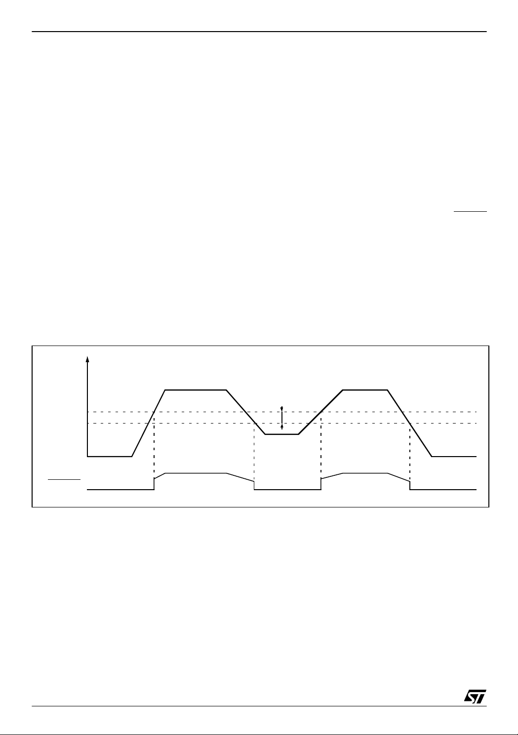
6.4.3.2 Clock detection Control
If the clock signal disappears (due to a broken or
disconnected resona tor...), the safe osc illator delivers a low frequency clock signal (f
SFOSC
allows the ST7 to perform some rescue operations.
Automatically, the ST7 clock source switches back
from the safe o scillator (f
source (f
) recovers.
OSC
When the internal clock (f
oscillator (f
), the application software is noti-
SFOSC
) if the main clock
SFOSC
) is driven by the safe
CPU
fied by hardware setting the CSSD bit i n the SICSR register. An interrupt can be generated if the
OSC
).
CPU
) whi c h
). It
CSSIE bit has been previously set.
These two bits are described in the SICSR register
description.
6.4.4 Low Power Modes
Mode Description
WAIT
HALT
)
No effect on SI. CSS and AVD interrupts
cause the device to exit from Wait mode.
The SICSR register is frozen.
The CSS (including the safe oscillator) is
disabled until HALT mode is exited. The
previous CSS configuration resumes when
the MCU is woken up by an interrupt with
“exit from HALT mode” capability or from
the counter reset value when the MCU is
woken up by a RESET.
6.4.4.1 Interrupts
The CSS or AVD i nterrupt events generat e an interrupt if the corresponding Enable Control Bit
(CSSIE or AVDIE) is set and the interrupt mask in
the CC register is reset (RIM instruction).
Flag
Enable
Control
Bit
Interrupt Event
CSS event detection
(safe oscillator activated as main clock)
AVD event AVDF AVDIE Yes No
Event
CSSD CSSIE Yes No
Exit
from
Wait
Exit
from
Halt
Figure 16. Clock Filter Function
Clock Filter Function
f
OSC2
PLL ON
f
CPU
Clock Detection Function
f
OSC2
f
SFOSC
f
CPU
26/171
ST72260G, ST72262G, ST72264G
SYSTEM INTEGRITY MANAGEMENT (Cont’d)
6.4.5 Register Description SYSTEM INTEGRITY (SI) CONTROL/ STATUS REGISTER (SICSR)
Read/Write
Reset Value: 000x 000x (00h)
70
AVDIEAVDFLVD
0
RF
CSSIECSSDWDG
0
RF
Bit 7 = Reserved, always read as 0.
Bit 6 = AVDIE
Voltage Detector interrupt enable
This bit is set and cleared by software. It enables
an interrupt to be generated when the AVDF flag
changes (toggles). The pending interrupt information is automatically cleared when software enters
the AVD interrupt routine.
0: AVD interrupt disabled
1: AVD interrupt enabled
Bit 5 = AVDF
Voltage Detector flag
This read-only bit is set and cleared by hardware.
If the AVDIE bit is set, an interrupt request is generated when the AVDF bit changes value.
over V
0: V
DD
under V
1: V
DD
Bit 4 = LV DRF
IT+(AVD)
threshold
IT-(AVD)
threshold
LVD reset flag
This bit indicates that the last Reset was generated by the LVD block. It is set by hardware (LVD reset) and cleared by software (writing zero). See
WDGRF flag description for more details. When
the LVD is disabled by OPTION BYTE, the LVDRF
bit value is undefined.
Bit 3 = Reserved, must be kept cleared.
Bit 2 = CSSIE
Clock security syst. interrupt enable
This bit enables the interrupt when a disturbance
is detected by the Clock Security System (CSSD
bit set). It is set and cleared by software.
0: Clock security system interrupt disabled
1: Clock security system interrupt enabled
When the CSS is di sabled by O PTIO N B YTE, t he
CSSIE bit has no effect.
Bit 1 = CSSD
Clock security system detecti o n
This bit indicates that the safe oscillator of the
Clock Security System block has been selected by
hardware due to a dist urbance on the main clock
signal (f
). It is set by hardware and c lea red by
OSC
reading the SICSR register when the original oscillato r recove rs.
0: Safe oscillator is not active
1: Safe oscillator has been activated
When the CSS is di sabled by O PTIO N B YTE, t he
CSSD bit value is forced to 0.
Bit 0 = WDGRF
Watchdog reset flag
This bit indicates that the last Reset was generated by the Watchdog p eripheral. It is set by hardware (watchdog reset) and cleared by software
(writing zero) or an LVD Reset (to ensure a stable
cleared state of the WDGRF flag when CPU
starts).
Combined with the LVDRF flag information, the
flag description is given by the following table.
RESET Sources LVDRF WDGRF
External RESET pin 0 0
Watchdog 0 1
LVD 1 X
Application Notes
The LVDRF flag is not cleared when another RESET type occurs (external or watchdog), the
LVDRF flag remains set to keep t race of the original failure. In this case, a watchdog reset can be
detected by software while an external reset can
not.
Address
(Hex.)
0025h
Register
Label
SICSR
Reset Value 0
76543210
AVDIE0AVDF0LVDRF
x0
CSSIE0CSSD0WDGRF
x
27/171
ST72260G, ST72262G, ST72264G
7 INTERRUPTS
7.1 INTRODUCTION
The ST7 enhanced interrupt management provides the following features:
■ Hardware interrupts
■ Software interrupt (TRAP)
■ Nested or concurrent interrupt management
with flexible interrupt priority and level
management:
– Up to 4 software programmable nesting levels
– Up to 16 interrupt vectors fixed by hardware
– 2 non-maskable events: RESET and TRAP
This interrupt management is based on:
– Bit 5 and bit 3 of the CPU CC register (I1:0),
– Interrupt software priority registers (ISPRx),
– Fixed interrupt vector addresses located at the
high addresses of the memory map (FFE0h to
FFFFh) sorted by hardware priority order.
This enhanced interrupt controller guarantees full
upward compatibility with the standard (not nested) ST7 interrupt controller.
7.2 MASKI NG AN D PROC ESSING FLOW
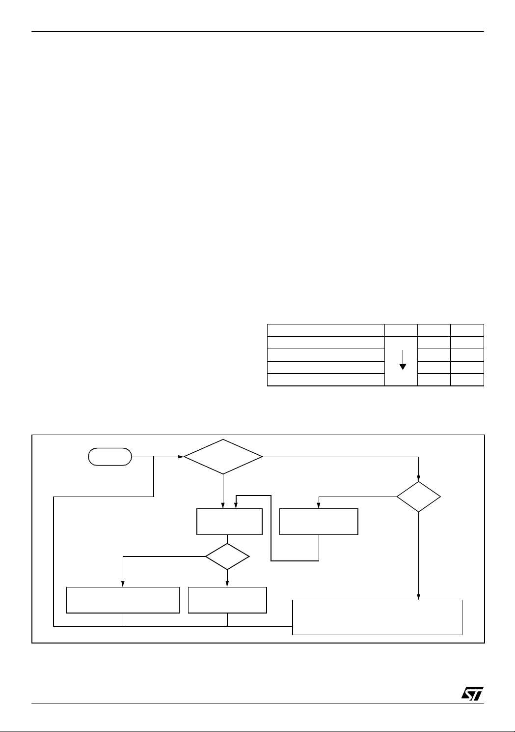
The interrupt masking is managed by the I1 and I0
bits of the CC register and the ISPRx registers
which give the interrupt software priority level of
each interrupt vector (see Table 4). The proc essing flow is shown in Figure 17
When an interrupt request has to be serviced:
– Normal processing is suspended at the end of
the current instruction execution.
– The PC, X, A and CC registers are saved onto
the stack.
– I1 and I0 bits of CC register are set according to
the corresponding values in the ISPRx registers
of the serviced interrupt vector.
– The PC is then loaded with the interrupt vector of
the interrupt to service and the first instruction of
the interrupt service routine is fetched (refer to
“Interrupt Mapping” table for vector addresses).
The interrupt service routine should end with the
IRET instruction which causes the cont ents of the
saved registers to be recovered from the stack.
Note: As a consequence of the IRET instruction,
the I1 and I0 bits will be restored from the stack
and the program in the previous level will resume.
Table 4. Interrupt Software Priority Levels
Interrupt software priority Le vel I1 I0
Level 0 (main) Low
Level 1 0 1
Level 2 0 0
Level 3 (= interrupt disable) 1 1
High
10
Figure 17. Inte rru pt P rocessing Flowchart
RESET
RESTORE PC, X, A, CC
FROM STACK
28/171
PENDING
INTERRUPT
N
FETCH NEX T
INSTRUCTION
Y
“IRET”
N
EXECUTE
INSTRUCTION
Y
THE INTERRUPT
STAYS PENDING
Interrupt has the same or a
lower software priority
than current one
STACK PC, X, A, CC
LOA D I1:0 FROM IN TERR UPT SW REG .
LOAD PC FROM INTERRUPT VECTOR
I1:0
softwarepriorit y
than current one
Interrupt has a higher
INTERRUPTS (Cont’d)
ST72260G, ST72262G, ST72264G
Servicing Pe nding Interrup t s
As several interrupts can b e pending at the sam e
time, the interrupt to be taken into account is determined by the following two-step process:
– the highest software priority interrupt is serviced,
– if several interrupts have the same software pri-
ority then the interrupt with the highest hardware
priority is serviced first.
Figure 18 describes this decision process.
Figure 18. Priority Decision Process
PENDING
INTERRUPTS
Same
HIGHEST HARDWARE
PRIORITY SERVICED
SOFTWARE
PRIORITY
HIGHEST SOFTWARE
PRIORITY SERVICED
Different
When an interrupt request is not serviced immediately, it is latched and then processed when its
software priority combined with the hardware priority becomes the highest one.
Note 1: The hardware priority is exclusive while
the software one is not. This allows the previ ous
process to succeed with only one interrupt.
Note 2: RESET and TRAP are non-maskable and
they can be considered as having the highest software priority in the decision process.
Different Interrupt Vector Sources
Two interrupt source types are managed by the
ST7 interrupt controller: the non-maskable type
(RESET and TRAP) and the maskable type (external or from internal peripherals).
Non-Maskable Sources
These sources are processed regardless of the
state of the I1 and I0 bits of the CC register (see
Figure 17). After stacking the PC, X, A and CC
registers (except for RESET), the corresponding
vector is loaded in the PC re gister and the I 1 and
I0 bits of the CC are set to disable interrupts (level
3). These sources allow the processor to exit
HALT mode.
■ TRAP (Non Maskable Software Interrupt)
This software interrupt is serviced when the TRAP
instruction is executed. It will be serviced according to the flowchart on Figure 17 as a TLI.
■ RESET
The RESET source has the highest priority in the
ST7. This means that the first current routine has
the highest software priority (level 3) and the highest hardware priority.
See the RESET chapter for more details.
Maskable Sources
Maskable interrupt vect or sourc es can be serviced
if the corresponding interrupt is e nabled and if its
own interrupt software priority (in ISPRx registers)
is higher than the one currently being serviced (I1
and I0 in CC regist er). If any of these two conditions is false, the interrupt is la tched and thus remains pending.
■ External Interrupts
External interrupts allow the processor to exit from
HALT low power mode.
External interrupt sensitivity is software selectable
through the Miscellaneous registers (MISCRx).
External interrupt triggered on edge will be latched
and the interrupt request automatically cleared
upon entering the interrupt service routine.
If several input pins of a grou p connected to the
same interrupt vector request an interrupt simultaneously, the interrupt vector w ill be se rv iced. Software can read the pin levels to identify which
pin(s) are the source of the interrupt.
If several input pins are selected simultaneously
as interrupt source, these are logically NANDed.
For this reason if o ne of the interrupt pins i s tied
low, it masks the other ones.
■ Peripheral Interrupts
Usually the peripheral interrupts cause the MCU to
exit from HALT mode except those mentioned in
the “Interrupt Mapping” table.
A peripheral interrupt occurs when a specific flag
is set in the peripheral status registers and if the
corresponding enable bit is set in the peripheral
control register.
The general sequence for clearing an interrupt is
based on an access to the status register followed
by a read or write to an associated register.
Note: The clearing sequence resets the internal
latch. A pending interrupt (i.e. waiting for being
serviced) will therefore be lost if the clear sequence is executed.
29/171
ST72260G, ST72262G, ST72264G
INTERRUPTS (Cont’d)
7.3 INTERRUPTS AND LOW POWER MODES
All interrupts allow the processor to exit the WAIT
low power mode. On the contrary, only external
and other specified interrupts allow the processor
to exit the HALT modes (see column “Exit from
HALT” in “Interrupt Mapping” table). When several
pending interrupts are present while exiting HALT
mode, the first one serviced can only be an interrupt with exit from HALT mode capability and it is
selected through the same decision process
shown in Figure 18.
Note: If an interrupt, that is not able to Exit from
HALT mode, is pending with the highest priority
when exiting HALT mode, this interrupt is serviced
after the first one serviced.
Figure 19. Concurren t Int errupt Management
IT1
TLI
IT3
IT0
TLI
IT1
RIM
IT2
IT1
IT4
IT2
HARDWARE PRIORITY
MAIN
11 / 10
7.4 CONCURRENT & NESTED MANAGEMENT
The following Figure 19 and Figure 20 show two
different interrupt management modes. The first is
called concurrent mode and does not allow an interrupt to be interrupted, unlike the nested mode in
Figure 20. The interrupt hardware priority is given
in this order from the l owest to the highest: MAIN,
IT4, IT3, IT2, IT1, IT0. The software priority is given for each interrupt.
Warning: A stack overflow may occur without notifying the software of the failure.
Note: TLI (Top Level Interrupt) is not available in
thi s product.
SOFTWARE
PRIORITY
LEVEL
IT0
IT3
IT4
MAIN
3
3
3
3
3
3
3/0
I1
11
11
11
11
11
11
10
I0
USED STACK = 10 BYTES
Figure 20. Nested Interrupt Management
IT2
IT1
IT4
IT1
IT2
RIM
HARDWARE PRIORITY
MAIN
TLI
IT3
IT4 IT4
IT0
TLI
11 / 10
30/171
IT0
IT3
IT1
SOFTWARE
PRIORITY
LEVEL
IT2
10
MAIN
I1 I0
3
3
2
1
3
3
3/0
11
11
00
01
11
11
USED STACK = 20 BYTES
 Loading...