

SGS Thomson Microelectronics ST72C104G2, ST72C104G1, ST72C254G2, ST72C254G1, ST72C216G1 Datasheet
...
8-BIT MCU WITH SINGLE VOLTAGE FLASH MEMORY,
ADC, 16-BIT TIMERS, SPI, I
■ Memories
– 4K or 8K bytes Program memory (ROM and
single voltage FLASH) with read-out protection and in-situ programming (remote ISP)
– 256 bytes RAM
■ Clock, Reset and Supply Management
– Enhanced reset system
– Enhanced low voltage supply supervisor with
3 programmable levels
– Clock sources: crystal/ceramic resonator os-
cillators or RC oscillators, external clock,
backup Clock Security System
– Clock-out capability
– 3 Power SavingModes: Halt, Wait and Slow
■ Interrupt Management
– 7 interrupt vectors plus TRAP and RESET
– 22 external interrupt lines (on 2 vectors)
■ 22 I/O Ports
– 22 multifunctional bidirectional I/O lines
– 14 alternate function lines
– 8 high sink outputs
■ 3 Timers
– Configurable watchdog timer
– Two 16-bittimers with: 2 input captures, 2out-
put compares,externalclock inputonone tim-
er, PWM and Pulse generator modes
(one only on ST72104Gx and ST72216G1)
■ 2 Communications Interfaces
– SPI synchronous serial interface
– I2C multimaster interface
(only on ST72254Gx)
■ 1 Analog peripheral
– 8-bit ADC with 6 input channels
(except on ST72104Gx)
ST72104G, ST72215G,
ST72216G, ST72254G
2
C INTERFACES
PRELIMINARY DATA
SDIP32
SO28
■ InstructionSet
– 8-bit data manipulation
– 63 basic instructions
– 17 main addressing modes
– 8 x 8 unsigned multiply instruction
– True bit manipulation
■ Development Tools
– Full hardware/softwaredevelopment package
Device Summary
Features ST72104G1 ST72104G2 ST72216G1 ST72215G2 ST72254G1 ST72254G2
Program memory - bytes 4K 8K 4K 8K 4K 8K
RAM (stack) - bytes 256 (128)
Peripherals
Operating Sup ply 3.0V to 5.5V
CPU Frequency Up to 8 MHz (with oscillator up to 16 MHz)
Operating Temp erature -40°C to +85°C (-40°C to +105/125°C optional)
Packages SO28 / SDIP 32
Watchdog timer,
One 16-bit timer,
SPI
Watchdog timer,
One 16-bit timer,
SPI, ADC
Watchdog timer,
Two 16-bit timers,
SPI, ADC
Watchdog timer,
Two 16-bit timers,
SPI, I C, ADC
Rev. 2.2
February 2000 1/135
This ispreliminary information on anew product in development or undergoing evaluation. Details are subject tochange without notice.
1

Table of Contents
1 INTRODUCTION . . . . . . . . . . . . . . . . . . . . . ......................................... 6
2 PIN DESCRIPTION . . . . . . . . . . . . ................................................ 7
3 REGISTER & MEMORY MAP . . . ................................................10
4 FLASH PROGRAM MEMORY . . . . . . . . . . . . . . . . . ................................. 13
4.1 INTRODUCTION . ...................................................... 13
4.2 MAIN FEATURES . . . . . . . . . . . . . . . . . . . . . . . . . . . . . . . . . . .................... 13
4.3 STRUCTURAL ORGANISATION . . . . . . . . . . . . . . . ........................... 13
4.4 IN-SITU PROGRAMMING (ISP) MODE . .................................... 13
4.5 MEMORY READ-OUT PROTECTION . . . . . ................................. 13
5 CENTRAL PROCESSING UNIT . . ............................................... 14
5.1 INTRODUCTION . ...................................................... 14
5.2 MAIN FEATURES . . . . . . . . . . . . . . . . . . . . . . . . . . . . . . . . . . .................... 14
5.3 CPU REGISTERS . . . . . . . . . . . . . . . . . . . . . ................................. 14
6 SUPPLY, RESET AND CLOCK MANAGEMENT . . . . ................................17
6.1 LOW VOLTAGE DETECTOR (LVD) . . . . . . . .................................18
6.2 RESET SEQUENCE MANAGER (RSM) . . . . . ................................19
6.2.1 Introduction . . . .................................................... 19
6.2.2 Asynchronous External RESET pin . . . . . . . . . . . . . . . . . . . . . . . . . . . . . ........ 20
6.2.3 Internal Low Voltage Detection RESET . . . . . . . . . . . . . . . . . . . . . . . . . . ........20
6.2.4 Internal Watchdog RESET . . . . . . . . . . .................................. 20
6.3 MULTI-OSCILLATOR (MO) . . . . . . . . . . . . . . . ................................21
6.4 CLOCK SECURITY SYSTEM (CSS) . . . . . . . . ................................22
6.4.1 Clock Filter Control . . ...............................................22
6.4.2 Safe Oscillator Control . . . . ...........................................22
6.4.3 Low Power Modes . . ............................................... 22
6.4.4 Interrupts . . . . . . . . . . . . . . . . . . . . . . . . ................................. 22
6.5 CLOCK RESET AND SUPPLY REGISTER DESCRIPTION (CRSR) . . . . . . . ........ 23
6.6 MAIN CLOCK CONTROLLER (MCC) . . . . . . . . . . . . ........................... 24
7 INTERRUPTS . . ............................................................. 25
7.1 NON MASKABLE SOFTWARE INTERRUPT . . . . . . ........................... 25
7.2 EXTERNAL INTERRUPTS . . . . . . . . . . . . . .................................. 25
7.3 PERIPHERAL INTERRUPTS . . ........................................... 25
8 POWER SAVING MODES . . . . . . . . . . ...........................................27
8.1 INTRODUCTION . ...................................................... 27
8.2 SLOW MODE . . . . . . . . . . . . . . ...........................................27
8.3 WAIT MODE . . . . . . . . . . . ............................................... 28
8.4 HALT MODE . . . . . . . . . . . ...............................................29
9 I/O PORTS . . . . . . . . . . . . . . . . . . . . . . . . . . ........................................ 30
9.1 INTRODUCTION . ...................................................... 30
9.2 FUNCTIONAL DESCRIPTION . . . . ........................................30
9.2.1 Input Modes . . . . . . . . . . . . . . . . . . . . . . ................................. 30
9.2.2 Output Modes . . . . . . ............................................... 30
9.2.3 Alternate Functions . . ...............................................30
9.3 I/O PORT IMPLEMENTATION . . . . ........................................33
135
2/135
2

Table of Contents
9.4 LOW POWER MODES . . . . . . . . . . . . . . . . . ................................. 34
9.5 INTERRUPTS . . . . . . . . . . . . . . . . . . . . . . . . ................................. 34
9.6 REGISTER DESCRIPTION . . . . . . . . . .. . . . . . . . . . . . . . . . . . . . . . . . . . . . . ........ 34
10 MISCELLANEOUS REGISTERS . . . . . . . . . . . . . . . . . . . . . . . . . . . . . . . . . . .. . . . . . . . . . . . 36
10.1 I/O PORT INTERRUPT SENSITIVITY . . . . . . ................................36
10.2 I/O PORT ALTERNATE FUNCTIONS . . . . . .................................. 36
10.3 MISCELLANEOUS REGISTERDESCRIPTION . . . . . . . . . . . . . . . . . . . . . . . . . . . . . . . 37
11 ON-CHIP PERIPHERALS . . . . . . ............................................... 39
11.1 WATCHDOG TIMER (WDG) . . . . . . . . . . . . . . . . . . . ........................... 39
11.1.1Introduction . . . . ................................................... 39
11.1.2Main Features . . . . . . . . . . . . . . . . . . . . ................................. 39
11.1.3Functional Description . . . . . . . ........................................ 39
11.1.4Hardware Watchdog Option . . . . . . . . . . . ................................40
11.1.5Low Power Modes . . . ...............................................40
11.1.6Interrupts . . . . . . .. . . . . . .. . . . . . . . . . . ................................ 40
11.1.7Register Description . . . . . . . . . ........................................ 40
11.2 16-BIT TIMER . . . . . . . . . . . . . . . . . . . . . . . . . . . . . . . . . . . . . . . . . . . . . . . . . ........ 42
11.2.1Introduction . . . . ................................................... 42
11.2.2Main Features . . . . . . . . . . . . . . . . . . . . ................................. 42
11.2.3Functional Description . . . . . . . ........................................ 42
11.2.4Low Power Modes . . ............................................... 54
11.2.5Interrupts . . . . . ....................................................54
11.2.6Summary of Timer modes . . . . . . . . . . . . . . . . . ........................... 54
11.2.7Register Description . . . . . . . . . ........................................ 55
11.3 SERIAL PERIPHERAL INTERFACE (SPI) . .................................. 60
11.3.1Introduction . . . . ................................................... 60
11.3.2Main Features . . . . . . . . . . . . . . . . . . . . ................................. 60
11.3.3General description . . . . . . ...........................................60
11.3.4Functional Description . . . . . . . ........................................ 62
11.3.5Low Power Modes . . . ...............................................69
11.3.6Interrupts . . . . . ....................................................69
11.3.7Register Description . . . . . . . . . ........................................ 70
11.4 I2C BUS INTERFACE (I2C) . . . . . . . . . . ....................................73
11.4.1Introduction . . . . ................................................... 73
11.4.2Main Features . . . . . . . . . . . . . . . . . . . . ................................. 73
11.4.3General Description . . . . . . . . . ........................................73
11.4.4Functional Description . . . . . . . ........................................ 75
11.4.5Low Power Modes . . . ...............................................79
11.4.6Interrupts . . . . . . .. . . . . . .. . . . . . . . . . . ................................ 79
11.4.7Register Description . . . . . . . . . ........................................ 80
11.5 8-BIT A/D CONVERTER (ADC) ........................................... 86
11.5.1Introduction . . . . ................................................... 86
11.5.2Main Features . . . . . . . . . . . . . . . . . . . . ................................. 86
11.5.3Functional Description . . . . . . . ........................................ 86
11.5.4Low Power Modes . . ............................................... 87
11.5.5Interrupts . . . . . . .. . . . . . .. . . . . . . . . . . ................................ 87
11.5.6Register Description . . . . . . . . . ........................................ 88
3/135
3

ST72104G, ST72215G, ST72216G, ST72254G
12 INSTRUCTION SET . . . . . . . . . . . . . . . . . . . . . . . . .................................90
12.1 ST7 ADDRESSING MODES . . . . . . . . . . . . . . . . . . .. . . . . . . . . . . . . . . . . . . . . . . . . . . 90
12.1.1Inherent . . . . .. . . . . . . . . . . . . . . . . . . . ................................. 91
12.1.2Immediate . . ...................................................... 91
12.1.3Direct . ........................................................... 91
12.1.4Indexed (No Offset, Short,Long) . . . . . .................................. 91
12.1.5Indirect (Short, Long) . . . . . ...........................................91
12.1.6Indirect Indexed (Short, Long) . ........................................92
12.1.7Relative mode (Direct, Indirect) . . . . ....................................92
12.2 INSTRUCTION GROUPS . . . . . . . . . . . . . . . . . . .............................. 93
13 ELECTRICAL CHARACTERISTICS . . . . ......................................... 96
13.1 PARAMETER CONDITIONS . . . . . . . . .. . . . . . . .............................. 96
13.1.1Minimum and Maximum values ........................................96
13.1.2Typical values . . . . . . . . . . ...........................................96
13.1.3Typical curves . . . . . . . . . . . . . ........................................96
13.1.4Loading capacitor . . . . . . . . . . . . . . . . . .................................. 96
13.1.5Pin input voltage . . . . . . . . . . . . . . . . . . . . . . . . . . . . . . . . . . . . . . . . . . . . . . . . . . . 96
13.2 ABSOLUTE MAXIMUM RATINGS . . . . . . . . . . . . . . . . . . . . . . . . . . . . . . . . . . . . . . . . . 97
13.2.1Voltage Characteristics . . . . . . . . .. . . . . . .. . . . . . . . . . . . . . . . . . . . . . . . . . . . . . 97
13.2.2Current Characteristics . . . . . . . . . . . . . . . . .............................. 97
13.2.3Thermal Characteristics . . . . . . . . . .................................... 97
13.3 OPERATING CONDITIONS . . . . . . . . . . .................................... 98
13.3.1General Operating Conditions . . . . .................................... 98
13.3.2Operating Conditions with Low Voltage Detector (LVD) . .................... 99
13.4 SUPPLY CURRENT CHARACTERISTICS . . . ...............................101
13.4.1RUN and SLOW Modes . . . . . .......................................101
13.4.2WAIT and SLOW WAIT Modes . . . . . . . . . . . . . . . . . . . . . . . . . . . . . . . . ....... 102
13.4.3HALT Mode . . . . . . . . .............................................. 103
13.4.4Supply and Clock Managers . ........................................ 103
13.4.5On-Chip Peripherals . . . . . ..........................................103
13.5 CLOCK AND TIMING CHARACTERISTICS . . . . . . . . . . . . . . . . . . . . . . . ..........104
13.5.1General Timings . . . . . . . . . . . . . . . . . . . . . . . . . . . . . . . . . . . . . . . . . . . . . . . . . . 104
13.5.2External Clock Source . . . . . . .......................................104
13.5.3Crystal and Ceramic Resonator Oscillators . . . . .......................... 105
13.5.4RC Oscillators . . . . . . . . . . ..........................................106
13.5.5Clock Security System (CSS) . . . . .. . . . . . . . . . . . . . . . . . . . . . . . . . . . . . . . . . . 107
13.6 MEMORY CHARACTERISTICS . . . .......................................108
13.6.1RAM and Hardware Registers . . . . . . . . . . . . . . . . . . . . . . . . . .............. 108
13.6.2FLASH Program Memory . . . . .......................................108
13.7 EMC CHARACTERISTICS . . . . . . . . . . . . . . . . . . . . . . . . . . . .. . . . . . . . . . . . . .. . . . 109
13.7.1Functional EMS . . . . . .............................................. 109
13.7.2Absolute Electrical Sensitivity . . . . . . . . . . . . . . .......................... 110
13.7.3ESD Pin Protection Strategy . . . . . . . . . . . . . . . . . . . . . . . . . . . . . . . . . . . . . . . . . 112
13.8 I/O PORT PIN CHARACTERISTICS .......................................114
13.8.1General Characteristics . . . . . . . . . . . . ................................. 114
13.8.2Output Driving Current . . . . .......................................... 115
13.9 CONTROL PIN CHARACTERISTICS . . . . . ................................. 117
4/135

ST72104G, ST72215G, ST72216G, ST72254G
13.9.1Asynchronous RESET Pin . . . . . . . . . . . . . . . . . .......................... 117
13.9.2ISPSEL Pin ...................................................... 119
13.10 TIMER PERIPHERAL CHARACTERISTICS . . . . . . . . . . . . . . . . . . . . . . . . . . ....... 120
13.10.1Watchdog Timer . . . . . . . . . . . . . . . . . . . . . . . . . . . . . . . . . . . . . . . . . . ....... 120
13.10.216-Bit Timer . . . . . . . . . . . . . . . . . . . . . ................................ 120
13.11 COMMUNICATION INTERFACE CHARACTERISTICS . . . . . ................... 121
13.11.1SPI - Serial Peripheral Interface . . . . . . . . . . . . ..........................121
13.11.2I2C - Inter IC ControlInterface . . . . . . . . . . . . . . . . . . . . . . . . . . . . . ..........123
13.12 8-BIT ADC CHARACTERISTICS . . . . . . . . ................................. 124
14 PACKAGE CHARACTERISTICS . . . . . . ........................................ 126
14.1 PACKAGE MECHANICAL DATA . . . . . . . . . . . . ............................. 126
14.2 THERMAL CHARACTERISTICS . . . . . . . . . . . . . . . . . . . .. . ................... 127
14.3 SOLDERING AND GLUEABILITY INFORMATION . . . .. . . . . . . . . . . . . . . . . ....... 128
14.4 PACKAGE/SOCKET FOOTPRINT PROPOSAL . . . . . . . . . . . ................... 128
15 DEVICE CONFIGURATION AND ORDERING INFORMATION . . . . . . . . . . . . . . . . . . . . . . . 129
15.1 OPTION BYTES . . . ................................................... 129
15.2 DEVICE ORDERING INFORMATION AND TRANSFER OF CUSTOMER CODE . . . . 130
15.3 DEVELOPMENT TOOLS . . . . . . . . . . . . . . . . . . . . . .......................... 132
15.4 ST7 APPLICATION NOTES . . . . . . . . . . . . .................................133
15.5 TO GET MORE INFORMATION . . . .......................................133
16 SUMMARY OF CHANGES . ..................................................134
5/135
ST72104G, ST72215G, ST72216G, ST72254G
1 INTRODUCTION
The ST72104G, ST72215G, ST72216G and
ST72254G devices are members of the ST7 microcontroller family. They can be grouped as follows:
– ST72254G devices are designed for mid-range
applications with ADC and I C interface capabilities.
– ST72215/6G devices target the same range of
applications but without I C interface.
– ST72104G devices are for applications that do
not need ADC and I C peripherals.
All devices are based on a c ommon industrystandard 8-bit core, featuringan enhanced instruction set.
The ST72C104G, ST72C215G, ST72C216G and
ST72C254G versions feature single-voltage
FLASH memory with byte-by-byte In-Situ Programming (ISP) capability.
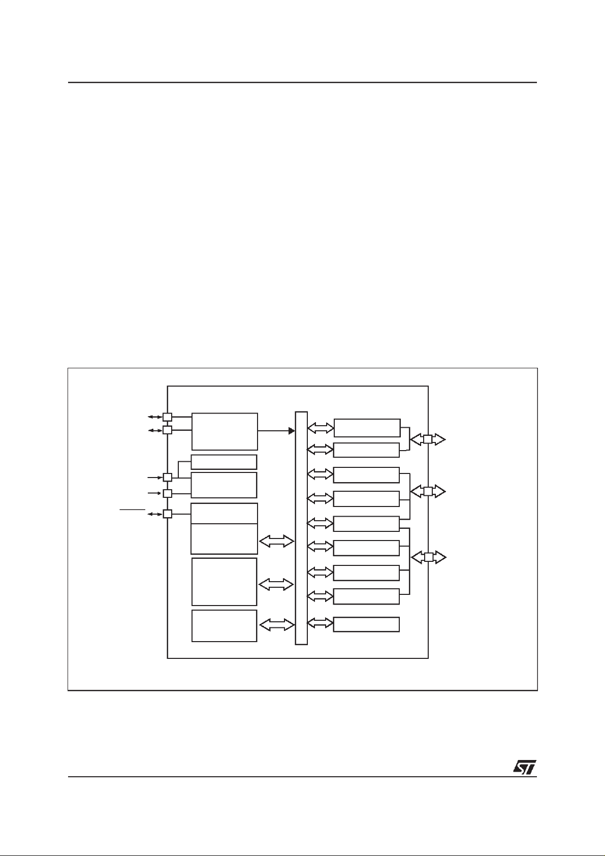
Figure 1. General Block Diagram
Internal
OSC1
OSC2
V
DD
V
RESE T
SS
MULTI O SC
+
CLOCK FILTE R
LVD
POWER
SUPPLY
CONTROL
8-BIT CORE
ALU
PROGRAM
MEMORY
(4 or 8K Bytes)
CLOCK
Under software control, all devices can be placed
in WAIT, SLOW, or HALT mode, reducing power
consumption when the application is in idle or
standby state.
The enhanced instruction set and a ddressing
modes of the ST7 offer both power and flexibilityto
software developers, enabling the design ofhighly
efficient andcompact application code. In addition
to standard 8-bit data management, all ST7 microcontrollers feature true bit manipulation, 8x8 unsigned multiplication and indirect addressing
modes.
For easy reference, all parametric data are located
in Section 13 on page 96.
I2C
PA7:0
(8 bits)
PB7:0
(8 bits)
PC5:0
(6 bits)
ADDRESS AND DATABUS
PORT A
SPI
PORT B
16-BIT TIMER A
PORT C
8-BIT AD C
16-BIT TIMER B
6/135
4
RAM
(256 Bytes)
WA TCHDOG
2 PIN DESCRIPTION
Figure 2. 28-Pin SO Package Pinout
ST72104G, ST72215G, ST72216G, ST72254G
RESET
OSC1
OSC2
SS/PB7
ISPCLK/SCK/PB6
ISPDATA/MISO/PB5
MOSI/PB4
OCMP2_A/PB3
ICAP2_A/PB2
OCMP1_A/PB1
ICAP1_A/PB0
AIN5/EXTCLK_A/PC5
AIN4/OCMP2_B/PC4
AIN3/ICAP2_B/PC3
Figure 3. 32-Pin SDIP Package Pinout
RESET
OSC1
OSC2
SS/PB7
ISPCLK/SCK/PB6
ISPDATA/MISO/PB5
MOSI/PB4
NC
NC
OCMP2_A/PB3
ICAP2_A/PB2
OCMP1_A/PB1
ICAP1_A/PB0
AIN5/EXTCLK_A/PC5
AIN4/OCMP2_B/PC4
AIN3/ICAP2_B/PC3
1
2
3
4
5
6
7
8
9
10
11
12
13
14
1
2
3
4
5
6
7
8
9
10
11
12
13
14
15
16
ei1 ei0
ei0 or ei1
ei0
ei1
ei0
ei1
ei0or ei1
V
28
DD
V
27
SS
ISPSEL
26
PA0 (HS)
25
PA1 (HS)
24
PA2 (HS)
23
PA3 (HS)
22
PA4 (HS)/SCLI
21
20
PA5 (HS)
19
PA6 (HS)/SDAI
PA7 (HS)
18
PC0/ICAP1_B/AIN0
17
PC1/OCMP1_B/AIN1
16
PC2/MCO/AIN2
15
(HS) 20mA highsink capability
eiX associated external interruptvector
V
32
31
30
29
28
27
26
25
24
23
22
21
20
19
18
17
DD
V
SS
ISPSEL
PA0 (HS)
PA1 (HS)
PA2 (HS)
PA3 (HS)
NC
NC
PA4 (HS)/SCLI
PA5 (HS)
PA6 (HS)/SDAI
PA7 (HS)
PC0/ICAP1_B/AIN0
PC1/OCMP1_B/AIN1
PC2/MCO/AIN2
(HS) 20mA highsink capability
eiX associated external interruptvector
7/135
5
ST72104G, ST72215G, ST72216G, ST72254G
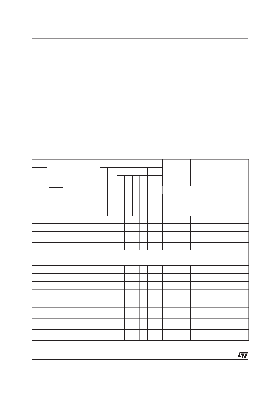
PIN DESCRIPTION (Cont’d)
For externalpin connection guidelines, refer to Section 13 ”ELECTRICAL CHARACTERISTICS” on page
96.
Legend / Abbreviationsfor Table 1:
Type: I = input, O = output, S = supply
Input level: A = Dedicated analog input
In/Output level: C = CMOS 0.3VDD/0.7VDD,
CT= CMOS 0.3VDD/0.7VDDwith input trigger
Output level: HS = 20mA high sink (on N-buffer only)
Port and control configuration:
– Input: float = floating, wpu = weak pull-up, int = interrupt1), ana = analog
– Output: OD = open drain2), PP = push-pull
Refer toSection 9 ”I/O PORTS” on page 30 for more details on the softwareconfiguration of the I/O ports.
The RESET configuration of each pin is shown in bold. This configuration is valid as long as thedevice is
in reset state.
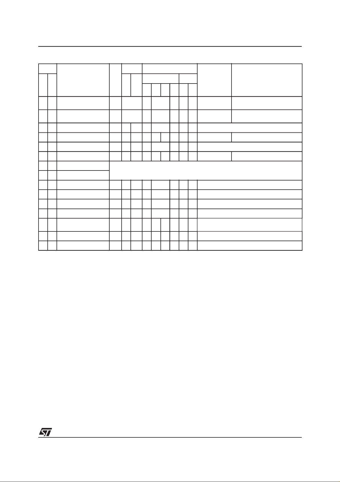
Table 1. Device Pin Description
Pin n°
Pin Name
SO28
SDIP32
1 1 RESET I/O C
2 2 OSC1
3 3 OSC2
4 4 PB7/SS I/O C
5 5 PB6/SCK/ISPCLK I/O C
6 6 PB5/MISO/ISPDATA I/O C
7 7 PB4/MOSI I/O C
8NC
9NC
10 8 PB3/OCMP2_A I/O C
11 9 PB2/ICAP2_A I/O C
12 10 PB1 /OCMP1_A I/O C
13 11 PB0 /ICAP1_A I/O C
14 12 PC5/EXTCLK_A/AIN5 I/O C
15 13 PC4/OCMP2_B/AIN4 I/O C
16 14 PC3/ ICAP2_B/AIN3 I/O C
17 15 PC2/MCO/AIN2 I/O C
3)
3)
Level Port / Control
Type
T
I
O
Input
T
T
T
T
T
T
T
T
T
T
T
T
Input Output
Output
float
X ei1 X X Port B7 SPI Slave Select (active low)
X ei1 X X Port B6 SPI Serial Clock or ISP Clock
X ei1 X X Port B5
X ei1 X X Port B4 SPI Master Out / Slave In Data
X ei1 X X Port B3 Timer A Output Compare 2
X ei1 X X Port B2 Timer A Input Capture 2
X ei1 X X Port B1 Timer A Output Compare 1
X ei1 X X Port B0 Timer A Input Capture 1
X ei0/ei1 X X Port C5
X ei0/ei1 X X Port C4
X ei0/ei1 X X X Port C3
X ei0/ei1 X X X Port C2
int
wpu
X X Toppriority nonmaskable interrupt (active low)
ana
OD
Not Connected
Main
Function
(after reset)
PP
External clock input or Resonator oscillator inverter input or resistor input for RC oscillator
Resonator oscillator inverter output or capacitor input for RC oscillator
Alternate Function
SPI Master In/ Slave OutData
or ISP Data
Timer A Input Clock or ADC
Analog Input 5
Timer B Output Compare 2 or
ADC Analog Input 4
Timer B Input Capture 2 or
ADC Analog Input 3
Main clock output (f
ADC Analog Input 2
CPU
)or
8/135
6
ST72104G, ST72215G, ST72216G, ST72254G
Pin n°
Level Port / Control
Pin Name
Type
SO28
SDIP32
18 16 PC1/OCMP1_B/AIN1 I/O C
19 17 PC0/ICAP1_B/AIN0 I/O C
20 18 PA7 I/O C
21 19 PA6 /SDAI I/O C
22 20 PA5 I/O C
23 21 PA4 /SCLI I/O C
Input
Output
T
T
HS X ei0 X X Port A7
T
HS X ei0 T Port A6 I2C Data
T
HS X ei0 X X Port A5
T
HS X ei0 T Port A4 I2C Clock
T
24 NC
25 NC
26 22 PA3 I/O C
27 23 PA2 I/O C
28 24 PA1 I/O C
29 25 PA0 I/O C
HS X ei0 X X Port A3
T
HS X ei0 X X Port A2
T
HS X ei0 X X Port A1
T
HS X ei0 X X Port A0
T
30 26 ISPSEL I C X
31 27 V
32 28 V
SS
DD
S Ground
S Main power supply
Input Output
Function
(after reset)
Main
float
wpu
int
ana
OD
PP
X ei0/ei1 X X X Port C1
X ei0/ei1 X X X Port C0
Not Connected
In situ programming selection (Should be tied
low in standard user mode).
Alternate Function
Timer B Output Compare 1 or
ADC Analog Input 1
Timer B Input Capture 1 or
ADC Analog Input 0
Notes:
1. In the interrupt input column, “eiX” defines the associated external interrupt vector. If the weak pull-up
column (wpu)is merged with theinterruptcolumn (int), then the I/O configuration is pull-up interruptinput,
else the configuration is floating interrupt input.
2. Inthe open drain output column, “T” defines a true open drain I/O(P-Buffer and protection diode to V
are not implemented). See Section 9 ”I/O PORTS” on page 30 and Section 13.8 ”I/O PORT PIN CHAR-
DD
ACTERISTICS” on page 114 for more details.
3. OSC1 andOSC2 pins connect a crystal or ceramic resonator, an external RC, or an external source to
the on-chiposcillatorsee Section 2 ”PIN DESCRIPTION” onpage 7 and Section 13.5 ”CLOCK AND TIMING CHARACTERISTICS” on page 104 for more details.
9/135
ST72104G, ST72215G, ST72216G, ST72254G
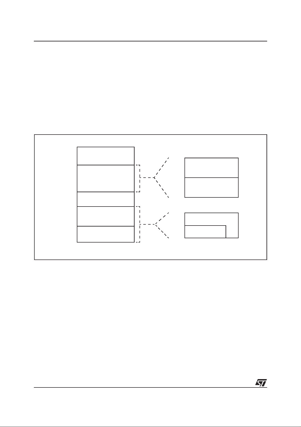
3 REGISTER & MEMORY MAP
As shown in the Figure 4, the MCU is capable of
addressing 64K bytes of memories and I/O registers.
The available memory locations consist of 128
bytes of register location, 256 bytes of RAM and
up to 8Kbytes of user program memory. The RAM
space includes up to 128 bytes for the stack from
0100h to 017Fh.
The highest address bytes contain the user reset
and interrupt vectors.
Figure 4. Memory Map
0000h
007Fh
0080h
017Fh
0180h
DFFFh
E000h
FFDFh
FFE0h
FFFFh
HW Registers
(see Table 2)
256 Bytes RAM
Reserved
Program Memory
(4K, 8 KBytes)
Interrupt & Reset Vectors
(see Table 5 on page 26)
IMPORTANT: Memory locations marked as “Reserved” must never be accessed. Accessing a reseved area can have unpredicable effects on the
device.
0080h
00FFh
0100h
017Fh
E000h
F000h
FFFFh
Short Addressing RAM
Zero page
(128 Bytes)
Stack or
16-bit Addressing RAM
(128 Bytes)
8 KBytes
4 KBytes
10/135
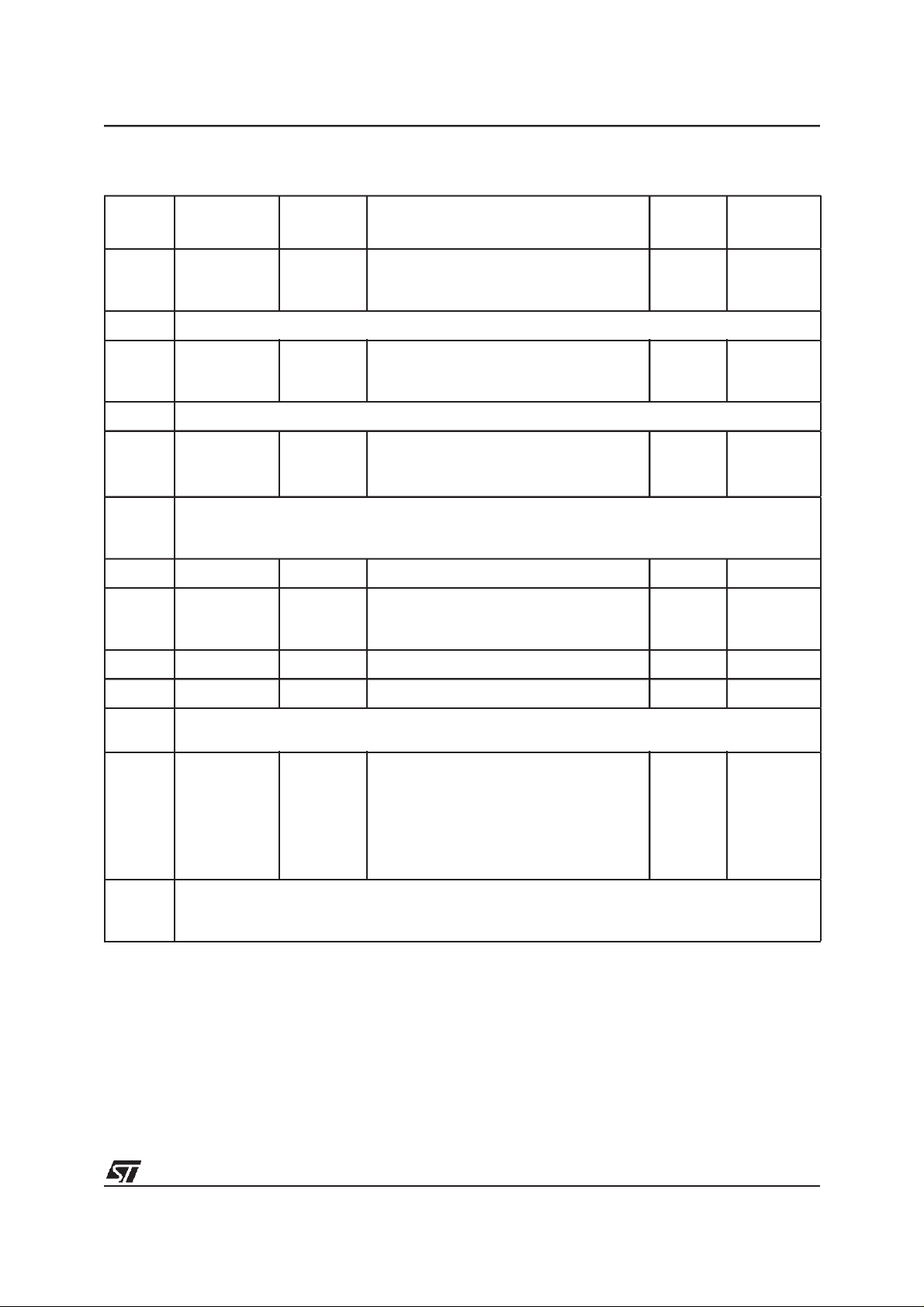
Table 2. Hardware Register Map
ST72104G, ST72215G, ST72216G, ST72254G
Address Block
0000h
0001h
Port C
0002h
Register
Label
PCDR
PCDDR
PCOR
Register Name
Port C Data Register
Port C Data Direction Register
Port C Option Register
Reset
Status
00h
00h
00h
1)
0003h Reserved (1 Byte)
0004h
0005h
0006h
Port B
PBDR
PBDDR
PBOR
Port B Data Register
Port B Data Direction Register
Port B Option Register
00h
00h
00h
1)
0007h Reserved (1 Byte)
0008h
0009h
000Ah
Port A
PADR
PADDR
PAOR
Port A Data Register
Port A Data Direction Register
Port A Option Register
00h
00h
00h
1)
000Bh
to
Reserved (21 Bytes)
001Fh
0020h MISCR1 Miscellaneous Register 1 00h R/W
0021h
0022h
0023h
SPI
SPIDR
SPICR
SPISR
SPI Data I/O Register
SPI Control Register
SPI Status Register
xxh
0xh
00h
0024h WATCHDOG WDGCR Watchdog Control Register 7Fh R/W
Remarks
2)
R/W
2)
R/W
2)
R/W
R/W
R/W
R/W.
R/W
R/W
R/W
R/W
R/W
Read Only
0025h CRSR Clock, Reset, Supply Control /Status Register 000x 000x R/W
0026h
0027h
0028h
0029h
002Ah
002Bh
002Ch
002Dh
002Eh
I2CCR
I2CSR1
2
C
I
I2CSR2
I2CCCR
I2COAR1
I2COAR2
I2CDR
Control Register
Status Register 1
Status Register 2
Clock Control Register
Own Address Register 1
Own Address Register 2
Data Register
Reserved (2 bytes)
00h
00h
00h
00h
00h
00h
00h
R/W
Read Only
Read Only
R/W
R/W
R/W
R/W
002Fh
to
Reserved (4 Bytes)
0030h
11/135
ST72104G, ST72215G, ST72216G, ST72254G
Address Block
0031h
0032h
0033h
0034h
0035h
0036h
0037h
0038h
0039h
003Ah
003Bh
003Ch
003Dh
003Eh
003Fh
0040h MISCR2 Miscellaneous Register 2 00h R/W
0041h
0042h
0043h
0044h
0045h
0046h
0047h
0048h
0049h
004Ah
004Bh
004Ch
004Dh
004Eh
004Fh
TIMER A
TIMER B
Register
Label
TACR2
TACR1
TASR
TAIC1HR
TAIC1LR
TAOC1HR
TAOC1LR
TACHR
TACLR
TAACHR
TAACLR
TAIC2HR
TAIC2LR
TAOC2HR
TAOC2LR
TBCR2
TBCR1
TBSR
TBIC1HR
TBIC1LR
TBOC1HR
TBOC1LR
TBCHR
TBCLR
TBACHR
TBACLR
TBIC2HR
TBIC2LR
TBOC2HR
TBOC2LR
Register Name
Timer A Control Register 2
Timer A Control Register 1
Timer A Status Register
Timer A Input Capture 1 High Register
Timer A Input Capture 1 Low Register
Timer A Output Compare 1 High Register
Timer A Output Compare 1 Low Register
Timer A Counter High Register
Timer A Counter Low Register
Timer A Alternate Counter High Register
Timer A Alternate Counter Low Register
Timer A Input Capture 2 High Register
Timer A Input Capture 2 Low Register
Timer A Output Compare 2 High Register
Timer A Output Compare 2 Low Register
Timer B Control Register 2
Timer B Control Register 1
Timer B Status Register
Timer B Input Capture 1 High Register
Timer B Input Capture 1 Low Register
Timer B Output Compare 1 High Register
Timer B Output Compare 1 Low Register
Timer B Counter High Register
Timer B Counter Low Register
Timer B Alternate Counter High Register
Timer B Alternate Counter Low Register
Timer B Input Capture 2 High Register
Timer B Input Capture 2 Low Register
Timer B Output Compare 2 High Register
Timer B Output Compare 2 Low Register
Reset
Status
00h
00h
xxh
xxh
xxh
80h
00h
FFh
FCh
FFh
FCh
xxh
xxh
80h
00h
00h
00h
xxh
xxh
xxh
80h
00h
FFh
FCh
FFh
FCh
xxh
xxh
80h
00h
Remarks
R/W
R/W
Read Only
Read Only
Read Only
R/W
R/W
Read Only
Read Only
Read Only
Read Only
Read Only
Read Only
R/W
R/W
R/W
R/W
Read Only
Read Only
Read Only
R/W
R/W
Read Only
Read Only
Read Only
Read Only
Read Only
Read Only
R/W
R/W
0050h
to
006Fh
0070h
0071h
0072h
to
007Fh
ADC
ADCDR
ADCCSR
Data Register
Control/Status Register
Reserved (32 Bytes)
Reserved (14 Bytes)
00h
00h
Read Only
R/W
Legend: x=undefined, R/W=read/write
Notes:
1. The contentsof the I/O port DR registers are readable only in output configuration. In input configuration, the values of the I/O pins are returnedinstead of the DR register contents.
2. The bits associated withunavailable pins must always keep their reset value.
12/135
4 FLASH PROGRAM MEMORY
ST72104G, ST72215G, ST72216G, ST72254G
4.1 INTRODUCTION
FLASH devices have a single voltage non-volatile
FLASH memory that may be programmed in-situ
(or plugged in a programming tool) on a byte-bybyte basis.
4.2 MAIN FEATURES
■ Remote In-Situ Programming (ISP) mode
■ Up to 16 bytes programmedin the same cycle
■ MTP memory (Multiple Time Programmable)
■ Read-out memory protection against piracy
4.3 STRUCTURAL ORGANISATION
The FLASH program memory is organised in a
single 8-bit wide memory block which can be used
for storing both code and data constants.
The FLASH program memory is mappedin the upper part ofthe ST7 addressing space and includes
the reset and interrupt user vector area .
4.4 IN-SITU PROGRAMMING (ISP) MODE
The FLASH program memory canbe programmed
using Remote ISP mode. This ISP mode allows
the contentsoftheST7program memory to be updated usingastandard ST7 programming tools after the device is mounted on the application board.
This feature can be implemented with a minimum
number of added components and board area impact.
An exampleRemote ISP hardware interface to the
standard ST7 programming tool is described below. For more details on ISP programming, refer to
the ST7 Programming Specification.
Remote ISP Overview
The Remote ISP mode is initiatedby a specific sequence on the dedicated ISPSEL pin.
The Remote ISP is performedin three steps:
– Selection of the RAM execution mode
– Download of Remote ISP codein RAM
– Execution ofRemote ISP code in RAM to pro-
gram the user program into the FLASH
Remote ISP hardware configuration
In Remote ISP mode, the ST7 has to be supplied
with power (VDDand VSS) and a clock signal (oscillator and application crystal circuit for example).
This mode needs five signals (plus the VDDsignal
if necessary) to be connected to the programming
tool. This signals are:
– RESET: device reset
–VSS: device ground power supply
– ISPCLK: ISP outputserial clock pin
– ISPDATA: ISP input serial data pin
– ISPSEL: Remote ISP modeselection. Thispin
must be connected to VSSon the application
board through a pull-down resistor.
If any of thesepins areused for other purposeson
the application, a serial resistor has to be implemented to avoid a conflict ifthe other deviceforces
the signal level.
Figure 5 shows a typical hardware interface to a
standard ST7 programming tool. For more details
on the pin locations, refer to the device pinout description.
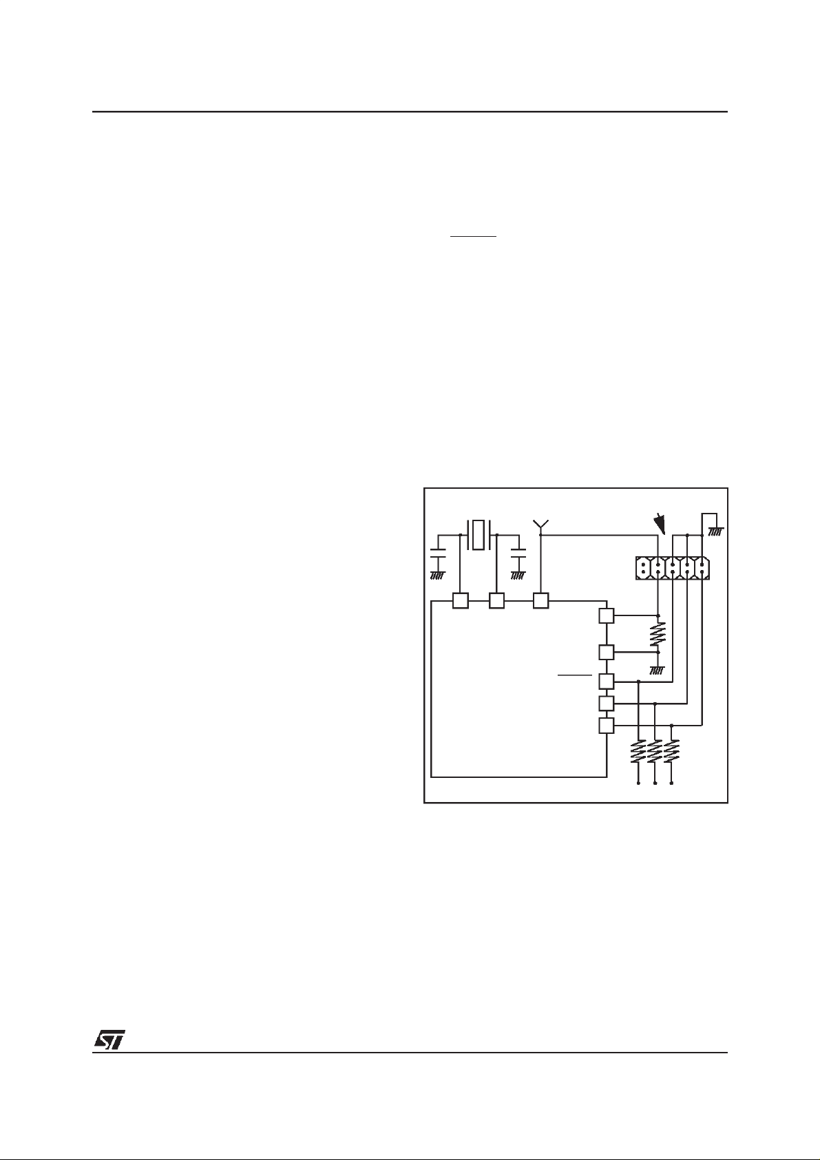
Figure 5. Typical Remote ISP Interface
HE10 CONNECTOR TYPE
TO PROGRAMMINGTOOL
ISPSEL
DD
V
V
RESET
ISPCLK
ISPDATA
10KΩ
SS
APPLICATION
1
47KΩ
C
XTAL
L0
OSC2
ST7
C
L1
OSC1
4.5 MEMORY READ-OUT PROTECTION
The read-out protection is enabled through an option bit.
For FLASH devices, when this option is selected,
the program and data stored in the FLASH memory are protected against read-out piracy (including
a re-write protection). When this protection option
is removed the entire FLASH program memory is
first automatically erased. However, the E2PROM
data memory (when available) can be protected
only with ROM devices.
13/135
ST72104G, ST72215G, ST72216G, ST72254G
5 CENTRAL PROCESSING UNIT
5.1 INTRODUCTION
This CPU has a full 8-bit architecture and contains
six internal registers allowing efficient 8-bit data
manipulation.
5.2 MAIN FEATURES
■ 63 basic instructions
■ Fast 8-bit by 8-bit multiply
■ 17 main addressing modes
■ Two 8-bit index registers
■ 16-bit stack pointer
■ Low power modes
■ Maskable hardware interrupts
■ Non-maskable software interrupt
5.3 CPU REGISTERS
The 6 CPU registers shown in Figure 6 are not
present in the memory mapping and are accessed
by specific instructions.
Figure 6. CPU Registers
70
RESET VALUE = XXh
70
RESET VALUE = XXh
70
RESET VALUE= XXh
Accumulator (A)
The Accumulator is an 8-bit general purpose register used to hold operands and the results of the
arithmetic and logic calculations and to manipulate
data.
Index Registers (X and Y)
In indexed addressing modes, these 8-bitregisters
are used to create either effective addresses or
temporary storage areas for data manipulation.
(The Cross-Assembler generates a precede instruction (PRE) to indicate that the following instruction refers to the Y register.)
The Y registeris not affectedby the interrupt automatic procedures (notpushed to and popped from
the stack).
Program Counter (PC)
The program counter is a 16-bit register containing
the address of the next instruction to be executed
by the CPU. It is made of two 8-bit registers PCL
(Program Counter Low which is the LSB) andPCH
(Program CounterHigh which is the MSB).
ACCUMULATOR
X INDEX REGISTER
Y INDEX REGISTER
15 8
RESET VALUE = RESET VECTOR @ FFFEh-FFFFh
15
RESET VALUE = STACKHIGHER ADDRESS
14/135
PCH
RESET VALUE =
7
70
1C11HI NZ
1X11X1XX
87 0
PCL
0
PROGRAM COUNTER
CONDITION CODE REGISTER
STACK POINTER
X = Undefined Value

ST72104G, ST72215G, ST72216G, ST72254G
CPU REGISTERS (Cont’d)
CONDITION CODE REGISTER (CC)
Read/Write
Reset Value: 111x1xxx
70
the interrupt routine. If the I bit is cleared by software in the interrupt routine, pending interrupts are
serviced regardless of the priority level of the current interrupt routine.
111HINZC
The 8-bit Condition Code register contains the interrupt mask and four flags representative of the
result ofthe instruction just executed. This register
can also be handled by the PUSH and POP instructions.
These bits can be individually tested and/or controlled by specific instructions.
Bit 4 = H
Half carry
.
This bit is set by hardware whena carryoccursbetween bits 3 and 4 of the ALU during an ADD or
ADC instruction. It is reset by hardware during the
same instructions.
0: No half carry has occurred.
1: A half carry has occurred.
This bit is tested using the JRH or JRNH instruction. The H bit is useful in BCD arithmetic subroutines.
Bit 3 = I
Interrupt mask
.
This bit is set by hardware when entering in interrupt or by software to disable all interrupts except
the TRAP software interrupt. This bit is cleared by
software.
0: Interrupts are enabled.
1: Interrupts are disabled.
This bit is controlledby the RIM, SIM and IRET instructions and is tested by the JRM and JRNM instructions.
Note: Interrupts requested while I is set are
latched and can be processed when I is cleared.
By default an interrupt routine is not interruptable
because the I bit is set by hardware when you enter it and resetby the IRETinstruction at the endof
Bit 2 = N
Negative
.
This bit is set and cleared by hardware. It is representative of the result sign of the last arithmetic,
logical or data manipulation. It is a copy of the 7
bit of the result.
0:Theresultof the last operation is positive or null.
1: The result of the last operation is negative
(i.e. the most significant bit is a logic 1).
This bit isaccessed bythe JRMI andJRPL instructions.
Bit 1 = Z
Zero
.
This bit is set and cleared by hardware. Thisbit indicates that the result of the last arithmetic, logical
or data manipulation is zero.
0: The result of the last operation is different from
zero.
1: The result of the last operation is zero.
This bit is accessed by the JREQ and JRNE test
instructions.
Bit 0 = C
Carry/borrow.
This bit is set and cleared by hardware and software. It indicates an overflow or an underflow has
occurred during the last arithmetic operation.
0: No overflow or underflow has occurred.
1: An overflow or underflow hasoccurred.
This bit is driven by the SCF and RCF instructions
and tested by the JRC and JRNC instructions. It is
also affected by the “bit test and branch”, shift and
rotate instructions.
th
15/135
ST72104G, ST72215G, ST72216G, ST72254G
CENTRAL PROCESSING UNIT (Cont’d)
Stack Pointer (SP)
Read/Write
Reset Value: 01 7Fh
15 8
00000001
70
0 SP6 SP5 SP4 SP3 SP2 SP1 SP0
The Stack Pointer is a 16-bit register which is always pointingto the next free location in the stack.
It isthen decremented after data has been pushed
onto the stack and incremented before data is
popped from the stack (see Figure 7).
Since the stack is 128 bytes deep, the 9th most
significant bits are forced by hardware. Following
an MCU Reset, or after a Reset Stack Pointer instruction (RSP), the Stack Pointer contains its reset value (the SP6 to SP0 bits areset) which is the
stack higher address.
The least significant byte of the Stack Pointer
(called S) can be directly accessed by a LD instruction.
Note: When the lower limit is exceeded, the Stack
Pointer wraps around to the stack upper limit, without indicating the stack overflow. The previously
stored information is then overwritten and therefore lost. The stack also wrapsin case of anunderflow.
The stack is used to save the return address during a subroutine call and the CPU context during
an interrupt. The user may also directly manipulate
the stack by meansof the PUSH and POP instructions. In the case of an interrupt, the PCL is stored
at the first location pointed to by the SP. Then the
other registers are stored in the next locations as
shown in Figure 7.
– When an interrupt is received, the SP is decre-
mented and the context is pushed on the stack.
– On return from interrupt, the SP is incremented
and the context is popped from thestack.
A subroutine call occupies twolocations and an interrupt five locations in the stack area.
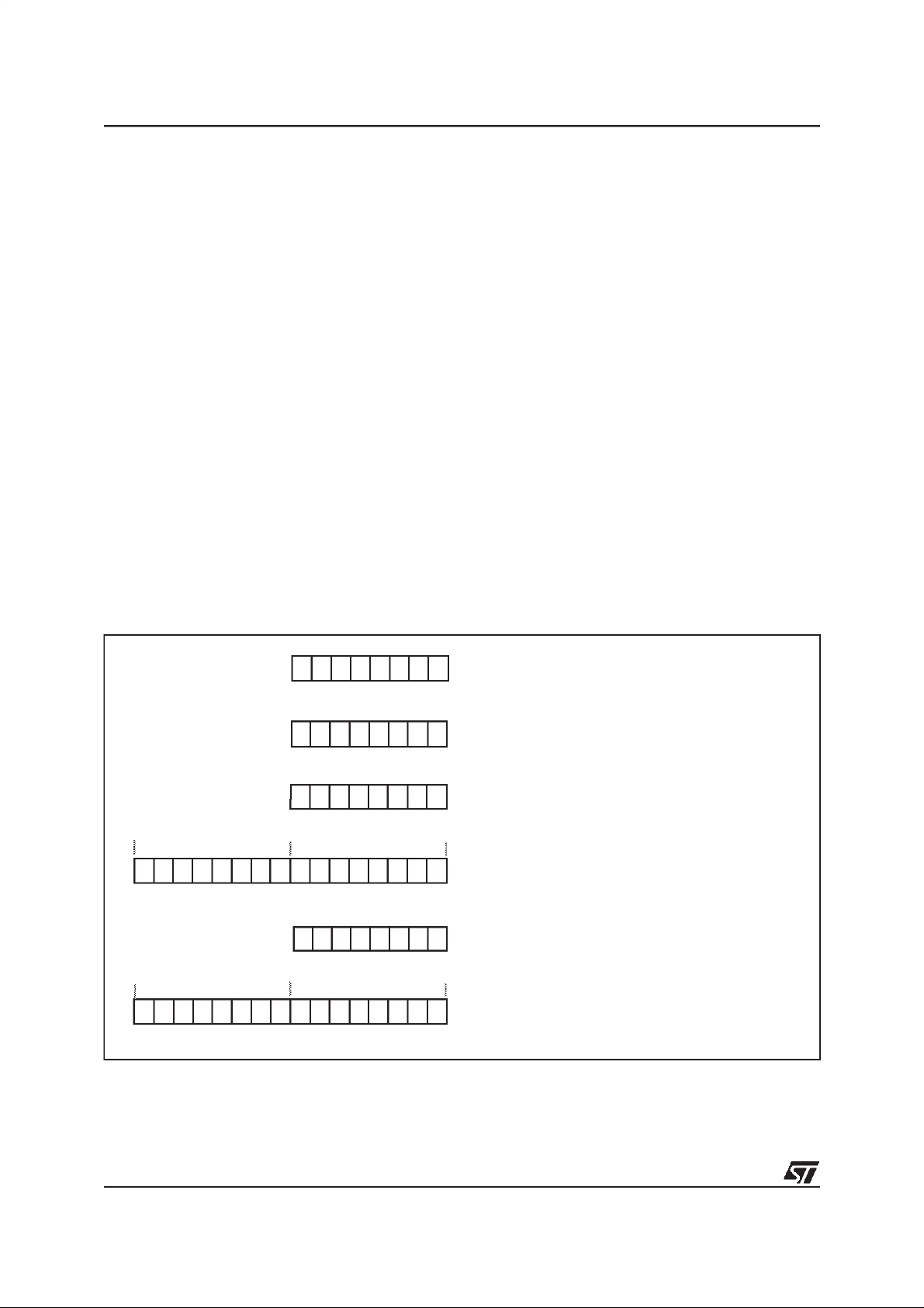
Figure 7. Stack Manipulation Example
@ 0100h
SP
@ 017Fh
CALL
Subroutine
SP
PCH
PCL
Stack Higher Address = 017Fh
Stack Lower Address =
Interrupt
Event
SP
CC
A
X
PCH
PCL
PCH
PCL
0100h
PUSH Y POP Y IRET
SP
Y
CC
A
X
PCH
PCL
PCH
PCL
CC
A
X
PCH
PCL
PCH
PCL
SP
PCH
PCL
RET
or RSP
SP
16/135
ST72104G, ST72215G, ST72216G, ST72254G
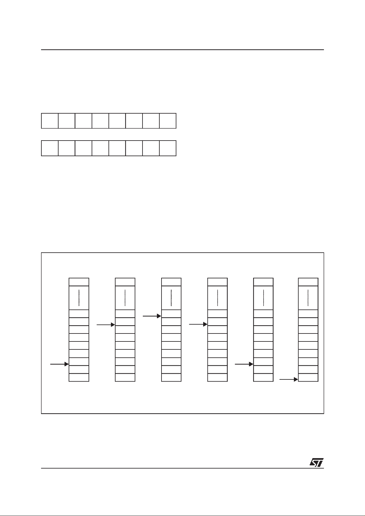
6 SUPPLY, RESET AND CLOCK MANAGEMENT
The ST72104G, ST72215G, ST72216G and
ST72254G microcontrollers include arange of utility features for securing the application in critical
situations (for example in case of a power brownout), and reducing the number of external components. An overview is shown in Figure 8.
See Section 13 ”ELECTRICAL CHARACTERISTICS” on page 96 for more details.
Main Features
■ Supply Manager with main supply low voltage
detection (LVD)
■ Reset Sequence Manager (RSM)
■ Multi-Oscillator (MO)
– 4 Crystal/Ceramic resonator oscillators
– 1 External RC oscillator
– 1 Internal RC oscillator
■ Clock Security System (CSS)
– Clock Filter
– Backup Safe Oscillator
Figure 8. Clock, Reset and Supply Block Diagram
MCO
OSC2
OSC1
RESET
VDD
VSS
MULTI-
OSCILLATOR
(MO)
RESET SEQUENCE
MANAGER
(RSM)
LOW VOLTAGE
DETECTOR
(LVD)
CLOCK SECURITYSYSTEM
CLOCK
FILTER
(CSS)
CRSR
SAFE
OSC
WATCHDOG
PERIPHERAL
FROM
f
OSC
MAIN CLOCK
CONTROLLER
(MCC)
LVD
f
CPU
CSS WDG
IE D00 0 0 RF RF
CSS INTERRUPT
17/135
ST72104G, ST72215G, ST72216G, ST72254G
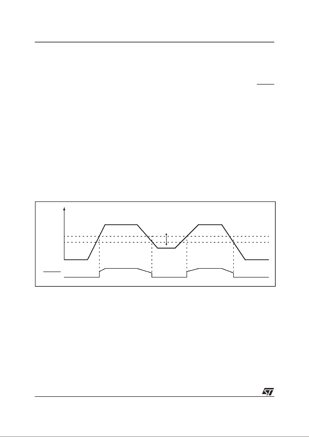
6.1 LOW VOLTAGE DETECTOR (LVD)
To allow the integration of power management
features in the application, the Low Voltage Detector function (LVD) generates a static reset when
the VDDsupply voltage is below a V
value. This means that it secures the power-up as
reference
IT-
well as the power-down keeping the ST7 in reset.
The V
than the V
referencevalue fora voltage drop is lower
IT-
referencevalue forpower-on in order
IT+
to avoid a parasitic reset when theMCUstarts running and sinks current on the supply (hysteresis).
The LVD Reset circuitry generates a reset when
VDDis below:
–V
when VDDis rising
IT+
–V
when VDDis falling
IT-
The LVD function is illustrated in the Figure 9.
Provided the minimum VDDvalue (guaranteed for
the oscillator frequency) is below V
, the MCU
IT-
can only be in two modes:
– under full software control
– in static safe reset
Figure 9. Low Voltage Detector vs Reset
V
DD
In these conditions, secure operation is always ensured for the application without the need for external reset hardware.
During aLow Voltage Detector Reset, the RESET
pin is held low, thus permitting the MCU to reset
other devices.
Notes:
1. The LVD allows the device to be used without
any external RESET circuitry.
2. Three different reference levels are selectable
through the option byte according to the application requirement.
LVD application note
Application software can detect a reset caused by
the LVD by reading the LVDRF bit in the CRSR
register.
This bit is set by hardware when a LVD reset is
generated and cleared by software (writing zero).
V
IT+
V
IT-
RESET
V
hyst
18/135
6.2 RESET SEQUENCE MANAGER (RSM)
ST72104G, ST72215G, ST72216G, ST72254G
6.2.1 Introduction
The reset sequence manager includes three RESET sources as shown in Figure 11:
■ External RESET source pulse
■ Internal LVD RESET (Low Voltage Detection)
■ Internal WATCHDOG RESET
These sources act on the RESET pin and it is always kept low during the delay phase.
The RESET service routine vector is fixed at addresses FFFEh-FFFFh in the ST7 memory map.
The basic RESET sequence consists of 3 phases
as shown in Figure 10:
■ Delay depending on the RESET source
■ 4096 CPU clock cycle delay
■ RESET vector fetch
Figure 11. Reset Block Diagram
V
RESET
DD
R
ON
f
CPU
The 4096 CPU clock cycle delay allows the oscillator to stabilise and ensures that recovery has
taken place from the Reset state.
The RESET vector fetch phase duration is 2 clock
cycles.
Figure 10. RESET Sequence Phases
RESET
DELAY
INTERNAL RESET
4096 CLOCK CYCLES
COUNTER
FETCH
VECTOR
INTERNAL
RESET
WATCHDOG RESET
LVD RESET
19/135
ST72104G, ST72215G, ST72216G, ST72254G
RESET SEQUENCE MANAGER (Cont’d)
6.2.2 Asynchronous External RESET pin
The RESETpin is both an input andan open-drain
output with integrated RONweak pull-up resistor.
This pull-up has no fixed value but varies in accordance with the input voltage. It can be pulled
low by external circuitry to reset the device. See
electrical characteristics section for more details.
A RESET signal originating from an external
source must have a duration of at least t
h(RSTL)in
in
order to be recognized. This detection is asynchronous and therefore the MCU can enter reset state
even in HALT mode.
The RESET pin is an asynchronous signal which
plays a major role in EMS performance. In a noisy
environment, it is recommended to follow the
guidelines mentioned in the electrical characteristics section.
Two RESET sequences can be associated with
this RESET source: short or long external reset
pulse (see Figure 12).
Starting from the external RESET pulse recognition, the device RESET pin acts as an output that
is pulled low during at least t
w(RSTL)out
.
Figure 12. RESET Sequences
6.2.3 Internal Low Voltage Detection RESET
Two different RESET sequences caused by the internal LVD circuitry can be distinguished:
■ Power-On RESET
■ Voltage Drop RESET
The device RESET pin acts as an output that is
pulled low when VDD<V
VDD<V
(falling edge) as shown in Figure 12.
IT-
The LVD filters spikes on VDDlarger than t
(rising edge) or
IT+
g(VDD)
to
avoid parasitic resets.
6.2.4 Internal Watchdog RESET
The RESET sequence generated by a internal
Watchdog counter overflow is shown in Figure 12.
Starting from the Watchdog counter underflow, the
device RESET pin acts as an output that is pulled
low during at least t
w(RSTL)out
.
EXTERNAL
RESET
SOURCE
RESET PIN
WATCHDOG
RESET
V
DD
V
IT+
V
IT-
SHORT EXT.
RESET
DELAY
LONG EXT.
RESET
RUN RUN
DELAY
t
h(RSTL)in
WATCHDOG UNDERFLOW
WATCHDOG
RESET
RUN
DELAY
t
w(RSTL)out
INTERNAL RESET (4096T
FETCH VECTOR
CPU
)
RUN
LVD
RESET
DELAY
RUN
t
w(RSTL)out
t
h(RSTL)in
20/135
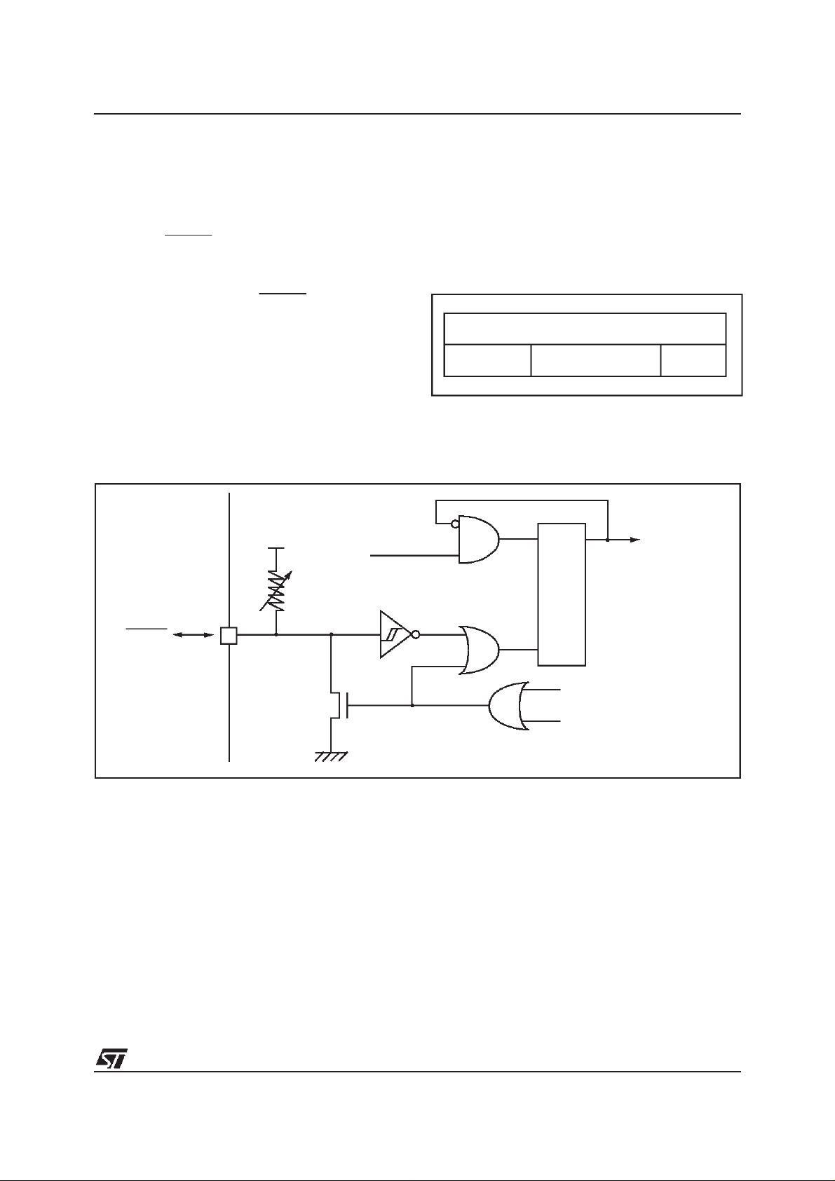
6.3 MULTI-OSCILLATOR (MO)
ST72104G, ST72215G, ST72216G, ST72254G
The main clock of the ST7 can be generated by
four different source types coming from the multioscillator block:
■ an external source
■ 4 crystal or ceramic resonator oscillators
■ an external RC oscillator
■ an internal high frequency RC oscillator
Each oscillator is optimized for a given frequency
range in terms of consumption and is selectable
through the option byte. The associated hardware
configuration are shown in Table 3. Refer to the
electrical characteristics section for more details.
External Clock Source
In this external clock mode, a clock signal (square,
sinus ortriangle) with~50% duty cycle has todrive
the OSC1 pinwhile theOSC2 pinis tied to ground.
Crystal/Ceramic Oscillators
This family of oscillators has theadvantage of producing a very accurate rate on the main clock of
the ST7. The selection within a list of 4 oscillators
with different frequency ranges has to be done by
option byte in order to reduce consumption. In this
mode of the multi-oscillator, the resonatorand the
load capacitors have to be placed as close as possible to the oscillator pins in order to minimize output distortion and start-up stabilization time. The
loading capacitance values must be adjusted according to the selected oscillator.
These oscillators are not stopped during the
RESET phase to avoid losing time in the oscillator
start-up phase.
Table 3. ST7 Clock Sources
Hardware Configuration
ST7
ST7
LOAD
CAPACITORS
ST7
External ClockCrystal/Ceramic ResonatorsExternal RC OscillatorInternal RC Oscillator
OSC1 OSC2
EXTERNAL
SOURCE
OSC1 OSC2
C
L1
OSC1 OSC2
R
EX
C
L2
C
EX
External RC Oscillator
This oscillator allows a low cost solution for the
main clockof the ST7 using only an external resistor and anexternal capacitor.The frequencyof the
external RC oscillator (in the range of some MHz.)
is fixed by the resistor and the capacitor values.
Consequently in this MO mode, the accuracy of
the clock is directly linked to the accuracy of the
discrete components.
Internal RC Oscillator
The internal RC oscillator mode is based on the
same principle as the external RC oscillator including the resistance and the capacitance of the device. This mode is the most cost effective one with
the drawback of a lower frequency accuracy. Its
frequency is in the range of several MHz.
In this mode, the two oscillator pins have to be tied
to ground.
ST7
OSC1 OSC2
21/135
ST72104G, ST72215G, ST72216G, ST72254G
6.4 CLOCK SECURITY SYSTEM (CSS)
The Clock Security System (CSS) protects the
ST7 against main clock problems. To allow the integration of the security features in the applications, itis based on a clock filter control and anInternal safe oscillator. The CSS can be enabled or
disabled by option byte.
6.4.1 Clock Filter Control
The clock filter is based on a clock frequency limitation function.
This filter function is able to detect and filter high
frequency spikes on the ST7 main clock.
If the oscillator is not working properly (e.g. working at a harmonic frequency of the resonator), the
current active oscillator clock can be totally filtered, and then no clock signal is available for the
ST7 from this oscillator anymore. If the original
clock source recovers, the filtering is stopped automatically and the oscillator supplies the ST7
clock.
6.4.2 Safe Oscillator Control
The safe oscillator of the CSS block is a low frequency back-up clock source (see Figure 13).
If the clock signal disappears (due to a broken or
disconnected resonator...) during a safe oscillator
period, the safe oscillator delivers a low frequency
clock signalwhich allows the ST7 to perform some
rescue operations.
Automatically, theST7 clock sourceswitches back
from the safe oscillator if the original clock source
recovers.
Limitation detection
The automatic safe oscillator selection is notified
by hardware setting the CSSD bit of the CRSR
register. An interrupt can be generated if the CSSIE bit has been previously set.
These two bits are described in the CRSR register
description.
6.4.3 Low Power Modes
Mode Description
WAIT
HALT
No effect on CSS. CSS interrupt cause the
device to exit from Wait mode.
The CRSR register is frozen. The CSS (including the safe oscillator) is disabled until
HALT mode is exited.The previous CSS
configuration resumes when the MCU is
woken up by aninterrupt with “exit from
HALT mode” capability or from the counter
reset value when the MCU is woken up by a
RESET.
6.4.4 Interrupts
The CSS interrupt event generates an interrupt if
the corresponding Enable Control Bit (CSSIE) is
set and the interrupt mask in the CC register is reset (RIM instruction).
Interrupt Event
CSS event detection
(safe oscillator activated as main clock)
Flag
Enable
Control
Bit
Event
CSSD CSSIE Yes No
Exit
from
Wait
Exit
from
Halt
Figure 13. Clock Filter Function and Safe Oscillator Function
f
/2
OSC
f
FUNCTION
CPU
CLOCK FILTER
f
/2
OSC
f
SFOSC
FUNCTION
f
CPU
SAFE OSCILLATOR
22/135
ST72104G, ST72215G, ST72216G, ST72254G
6.5 CLOCK RESET AND SUPPLY REGISTER DESCRIPTION (CRSR)
Read/Write
Reset Value: 000x 000x (XXh)
70
000
LVD
RF
CSSIECSSDWDG
0
RF
Bit 1 = CSSD
Clock security system detection
This bit indicates that the safe oscillator of the
clock security system block has been selected by
hardware due to a disturbance on the main clock
signal (f
). It is set by hardware and cleared by
OSC
reading the CRSR register when the originaloscillator recovers.
0: Safe oscillator is not active
Bit 7:5 = Reserved, always read as 0.
1: Safe oscillator has been activated
When the CSS is disabled by option byte, the
CSSD bit value is forced to 0.
Bit 4 = LVDRF
This bit indicates that the last RESET was generated by the LVD block. It is set by hardware (LVD
reset) and cleared by software (writing zero). See
WDGRF flag description for more details. When
the LVD is disabled by option byte, the LVDRF bit
value is undefined.
LVD reset flag
Bit 0 = WDGRF
Watchdog reset flag
This bit indicates that the last RESET was generated by the watchdog peripheral. It is set by hardware (Watchdog RESET) and cleared by software
(writing zero) or an LVD RESET (to ensure a stable cleared state of the WDGRF flag when the
CPU starts).
Bit 3 = Reserved, always read as 0.
Bit 2 = CSSIE
Clock security syst.interrupt enable
This bit enables the interrupt when a disturbance
is detected bythe clock security system (CSSD bit
set). It is set and cleared by software.
Combined with the LVDRF flag information, the
flag description is given by the following table.
RESET Sources LVDRF WDGRF
External RESET pin 0 0
Watchdog 0 1
LVD 1 X
0: Clock security system interrupt disabled
1: Clock security system interrupt enabled
Refer to Table 5, “Interrupt Mapping,” on page 26
for more details on the CSS interrupt vector. When
the CSS is disabled by option byte, the CSSIE bit
has no effect.
Application notes
The LVDRF flag is not cleared when another RESET type occurs (external or watchdog), the
LVDRF flagremains set to keep trace of the original failure.
In this case, a watchdog reset can be detected by
software while an external reset can not.
Table 4. Clock, Reset and Supply Register Map and Reset Values
Address
(Hex.)
0025h
Register
Label
CRSR
Reset Value 0 0 0
76543210
LVDRF
x0
CSSIE0CSSD0WDGRF
x
23/135
ST72104G, ST72215G, ST72216G, ST72254G
6.6 MAIN CLOCK CONTROLLER (MCC)
The Main Clock Controller (MCC) supplies the
clock for the ST7 CPU and its internal peripherals.
It allows SLOW power saving mode to be managed by the application.
All functions are managed by the Miscellaneous
register 1 (MISCR1).
The MCC block consists of:
■ A programmable CPU clock prescaler
■ A clock-out signal to supply external devices
The prescaler allows the selection of the main
clock frequency and is controlled by three bits of
the MISCR1: CP1, CP0 and SMS.
The clock-out capability consists of a dedicated
I/O port pin configurable as an f
drive external devices. It is controlled by the MCO
bit in the MISCR1 register.
See Section 10 ”MISCELLANEOUS REGISTERS” on page 36 for more details.
Figure 14. Main Clock Controller (MCC) Block Diagram
PORT
ALTERNATE
f
OSC
/2
MISCR1
FUNCTION
MCO ----
clockoutput to
CPU
CLOCK TO CAN
PERIPHERAL
MCO
SMSCP1 CP0
f
OSC
DIV2,4,8,16DIV 2
f
CPU
CPU CLOCK
TO CPU AND
PERIPHERALS
24/135

7 INTERRUPTS
ST72104G, ST72215G, ST72216G, ST72254G
The ST7 core may be interruptedby one oftwo different methods: maskable hardware interrupts as
listed in the Interrupt Mapping Table and a nonmaskable software interrupt (TRAP). The Interrupt
processing flowchart is shown in Figure 15.
The maskableinterrupts must be enabled clearing
the I bit in order to be serviced. However, disabled
interrupts may be latched and processed when
they are enabled (see external interrupts subsection).
When an interrupt has to be serviced:
– Normal processing is suspended at the end of
the current instruction execution.
– The PC, X, A and CC registers are saved onto
the stack.
– The I bit of the CC register is set to prevent addi-
tional interrupts.
– ThePC isthenloaded with the interrupt vectorof
the interruptto service and the first instruction of
the interrupt service routine is fetched (refer to
the Interrupt Mapping Tablefor vector addresses).
The interrupt service routine should finish with the
IRET instruction which causes the contents of the
saved registers to be recovered from thestack.
Note: As a consequence of the IRET instruction,
the I bit will be cleared and the main program will
resume.
Priority management
By default, a servicing interrupt cannot be interrupted because the I bit is set by hardware entering in interrupt routine.
In the case when severalinterrupts are simultaneously pending, an hardware priority defines which
one will be serviced first (see the Interrupt Mapping Table).
Interrupts and Low power mode
All interrupts allow the processor to leave the
WAIT low power mode. Only external and specifically mentioned interrupts allow the processor to
leave the HALT low power mode (refer to the “Exit
from HALT“ column in the Interrupt Mapping Table).
7.1 NON MASKABLE SOFTWARE INTERRUPT
This interrupt is entered when the TRAP instruction is executed regardless of the stateof theI bit.
It will be serviced according to the flowchart on
Figure 15.
7.2 EXTERNAL INTERRUPTS
External interrupt vectors can be loaded into the
PC register if the corresponding external interrupt
occurred and if the I bit is cleared. Theseinterrupts
allow the processor to leave the Halt low power
mode.
The external interrupt polarity is selected through
the miscellaneous register or interrupt register (if
available).
An external interrupt triggered on edge will be
latched and the interrupt request automatically
cleared upon entering the interrupt serviceroutine.
If several input pins, connected to the same interrupt vector, are configured as interrupts, their signals are logically ANDed beforeentering the edge/
level detection block.
Caution:The type of sensitivitydefinedin the Miscellaneous or Interrupt register (if available) applies to the ei source. In case of an ANDedsource
(as described on the I/O ports section), a low level
on an I/O pin configured as input with interrupt,
masks the interrupt requesteven in case of risingedge sensitivity.
7.3 PERIPHERAL INTERRUPTS
Different peripheral interrupt flags in the status
register are able to cause an interrupt when they
are active if both:
– The I bit of the CC register is cleared.
– Thecorresponding enable bit is setin thecontrol
register.
If any of these two conditions is false, the interrupt
is latched and thus remains pending.
Clearing an interrupt request is done by:
– Writing “0” to the corresponding bit in the status
register or
– Access tothe status registerwhile the flag isset
followed by a read or write of an associated register.
Note: the clearing sequence resets the internal
latch. A pending interrupt (i.e. waiting for being enabled) will therefore be lost ifthe clear sequence is
executed.
25/135
ST72104G, ST72215G, ST72216G, ST72254G
INTERRUPTS (Cont’d)
Figure 15. Interrupt Processing Flowchart
FROM RES ET
N
N
INTE RRUPT
PENDING?
Y
STACK PC, X, A, CC
SET I BIT
LOAD PC FROM INTERRUPT VECTO R
EXECU TE INSTRUCTION
RESTORE P C, X, A, CC FROM STACK
I BIT SET?
Y
FETCH NEXT INSTR UCTION
N
THIS CLEA RS I BIT BY DEFAULT
IRET?
Y
Table 5. Interrupt Mapping
N°
Source
Block
Description
RESET Reset
TRAP Software Interrupt no FFFCh-FFFDh
0 ei0 External Interrupt Port A7..0 (C5..0
1 ei1 External Interrupt Port B7..0 (C5..0
1
)
1
) FFF8h-FFF9h
Register
Label
N/A
Priority
Order
Highest
Priority
2 CSS Clock Filter Interrupt CRSR
3 SPI SPI Peripheral Interrupts SPISR FFF4h-FFF5h
4 TIMER A TIMER A Peripheral Interrupts TASR FFF2h-FFF3h
5 Not used FFF0h-FFF1h
6 TIMER B TIMER B Peripheral Interrupts TBSR no FFEEh-FFEFh
7 Not used FFECh-FFEDh
8 Not used FFEAh-FFEBh
9 Not used FFE8h-FFE9h
10 Not used FFE6h-FFE7h
11 I C I C Peripheral I nterrupt I2CSRx no FFE4h-FFE 5h
12 Not Used FFE2h-FFE 3h
13 Not Used FFE0h-FFE 1h
Lowest
Priority
Exit
from
HALT
Address
Vector
yes FFFEh-FFFFh
yes
FFFAh-FFFBh
FFF6h-FFF7h
no
Note
1. Configurable by option byte.
26/135
8 POWER SAVING MODES
ST72104G, ST72215G, ST72216G, ST72254G
8.1 INTRODUCTION
To give a large measure of flexibilitytotheapplication in terms of power consumption, three main
power saving modes are implemented in the ST7
(see Figure 16).
After a RESET the normal operating mode is selected by default (RUN mode). This mode drives
the device (CPU and embedded peripherals) by
means of a master clock which is based on the
main oscillator frequency divided by 2 (f
CPU
).
From Run mode, the different power saving
modes may be selected by setting the relevant
register bits or by calling the specific ST7 software
instruction whose action depends on the the oscillator status.
Figure 16. Power Saving Mode Transitions
High
RUN
SLOW
WAIT
8.2 SLOW MODE
This mode has two targets:
– To reduce powerconsumption bydecreasingthe
internal clock in the device,
– To adapt the internal clock frequency (f
the available supply voltage.
CPU
)to
SLOW mode is controlled by three bits in the
MISCR1 register: the SMS bit which enables or
disables Slow mode and two CPx bits whichselect
the internal slow frequency (f
CPU
).
In this mode, the oscillator frequency can bedivided by 4, 8, 16 or 32 instead of 2 in normal operating mode. The CPU and peripherals are clocked at
this lower frequency.
Note: SLOW-WAIT modeis activated when enterring the WAIT mode while the device is already in
SLOW mode.
Figure 17. SLOW Mode Clock Transitions
f
f
CPU
f
OSC
CP1:0
/2
/4 f
OSC
00 01
OSC
/8 f
OSC
/2
SLOW WAIT
HALT
Low
POWER CONSUMPTION
SMS
MISCR1
NEW SLOW
FREQUENCY
REQUEST
NORMAL RUN MODE
REQUEST
27/135
ST72104G, ST72215G, ST72216G, ST72254G
POWER SAVING MODES (Cont’d)
8.3 WAIT MODE
WAIT mode places the MCU in a low power consumption mode by stopping the CPU.
This power saving mode is selectedby calling the
“WFI” ST7 software instruction.
All peripherals remain active. During WAIT mode,
the I bit of theCC register is forced to 0, to enable
all interrupts. All other registers and memory remain unchanged. The MCU remains in WAIT
mode until an interrupt or Reset occurs, whereupon the Program Counter branches to the starting
address of the interrupt or Reset serviceroutine.
The MCU will remain in WAIT mode until a Reset
or an Interrupt occurs, causing it to wake up.
Refer to Figure18.
Figure 18. WAIT Mode Flow-chart
OSCILLATOR
WFI INSTRUCTION
N
INTERRUPT
Y
PERIPHERALS
CPU
IBIT
N
RESET
Y
OSCILLATOR
PERIPHERALS
CPU
IBIT
4096 CPU CLOCK CYCLE
DELAY
OSCILLATOR
PERIPHERALS
CPU
I BIT
ON
ON
OFF
0
ON
OFF
ON
1
ON
ON
ON
X
1)
FETCH RESET VECTOR
OR SERVICE INTERRUPT
Note:
1. Before servicing an interrupt, the CC register is
pushed on thestack. The I bit of the CC register is
set during the interrupt routine and cleared when
the CC register is popped.
28/135
POWER SAVING MODES (Cont’d)
ST72104G, ST72215G, ST72216G, ST72254G
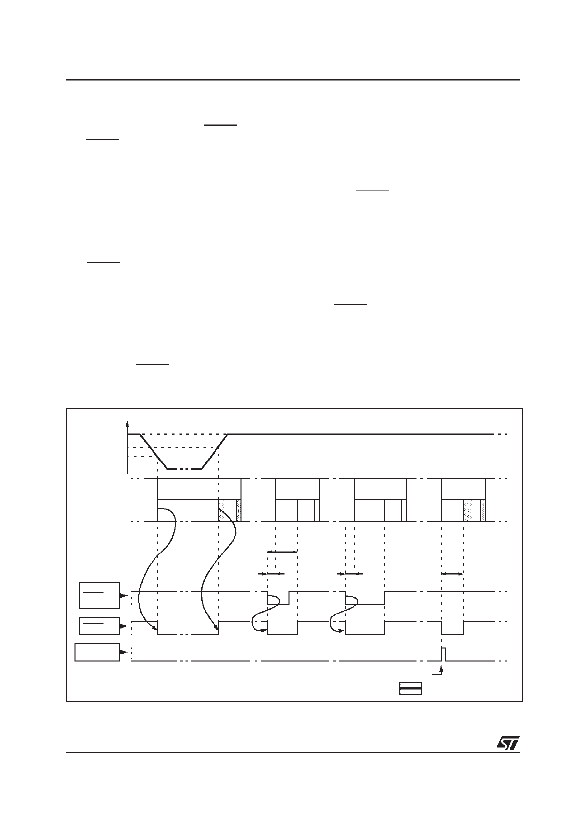
8.4 HALT MODE
The HALT mode is the lowest power consumption
mode of the MCU. It is entered by executing the
ST7 HALT instruction (see Figure 20).
The MCU can exit HALT mode on reception of either a specific interrupt (see Table 5, “Interrupt
Mapping,” on page 26) or a RESET. When exiting
HALT mode by means of a RESET or an interrupt,
the oscillator is immediately turned on and the
4096 CPU cycle delay is used to stabilize the oscillator. After the start up delay, the CPU resumes
operation by servicing the interrupt or by fetching
the reset vector which woke it up (see Figure 19).
When entering HALT mode, the I bit in the CC register is forced to 0 to enable interrupts. Therefore,
if an interrupt is pending, the MCU wakes immediately.
In the HALT mode the main oscillator is turned off
causing all internal processing to be stopped, including the operation of the on-chip peripherals.
All peripherals are not clocked except the ones
which get their clock supply from another clock
generator (such as an external or auxiliary oscillator).
The compatibility of Watchdog operation with
HALT mode is configured by the “WDGHALT” option bit of the option byte. The HALT instruction
when executed while the Watchdog system is enabled, can generate a Watchdog RESET (see
Section 15.1 ”OPTION BYTES” on page 129 for
more details).
Figure 19. HALT Mode Timing Overview
HALTRUN RUN
4096 CPU CYCLE
DELAY
Figure 20. HALT Mode Flow-chart
HALT INSTRUCTION
WDGHALT
1
WATCHDOG
RESET
N
INTERRUPT
Y
1)
ENABLE
0
OSCILLATOR
PERIPHERALS
CPU
IBIT
N
3)
OSCILLATOR
PERIPHERALS
CPU
IBIT
4096 CPU CLOCK CYCLE
OSCILLATOR
PERIPHERALS
CPU
IBIT
FETCH RESET VECTOR
OR SERVICE INTERRUPT
WATCHDOG
RESET
Y
DELAY
DISABLE
OFF
2)
OFF
OFF
0
ON
OFF
ON
1
ON
ON
ON
4)
X
HALT
INSTRUCTION
INTERRUPT
RESET
OR
FETCH
VECTOR
Notes:
1.WDGHALTis anoption bit. See option byte section for more details.
2.Peripheral clocked with an external clock source
can still be active.
3. Only some specific interrupts can exit the MCU
from HALT mode (such as external interrupt). Refer toTable 5, “Interrupt Mapping,” on page 26 for
more details.
4. Before servicing an interrupt, the CC register is
pushed on thestack. The I bit of the CC register is
set during the interrupt routine and cleared when
the CC register is popped.
29/135
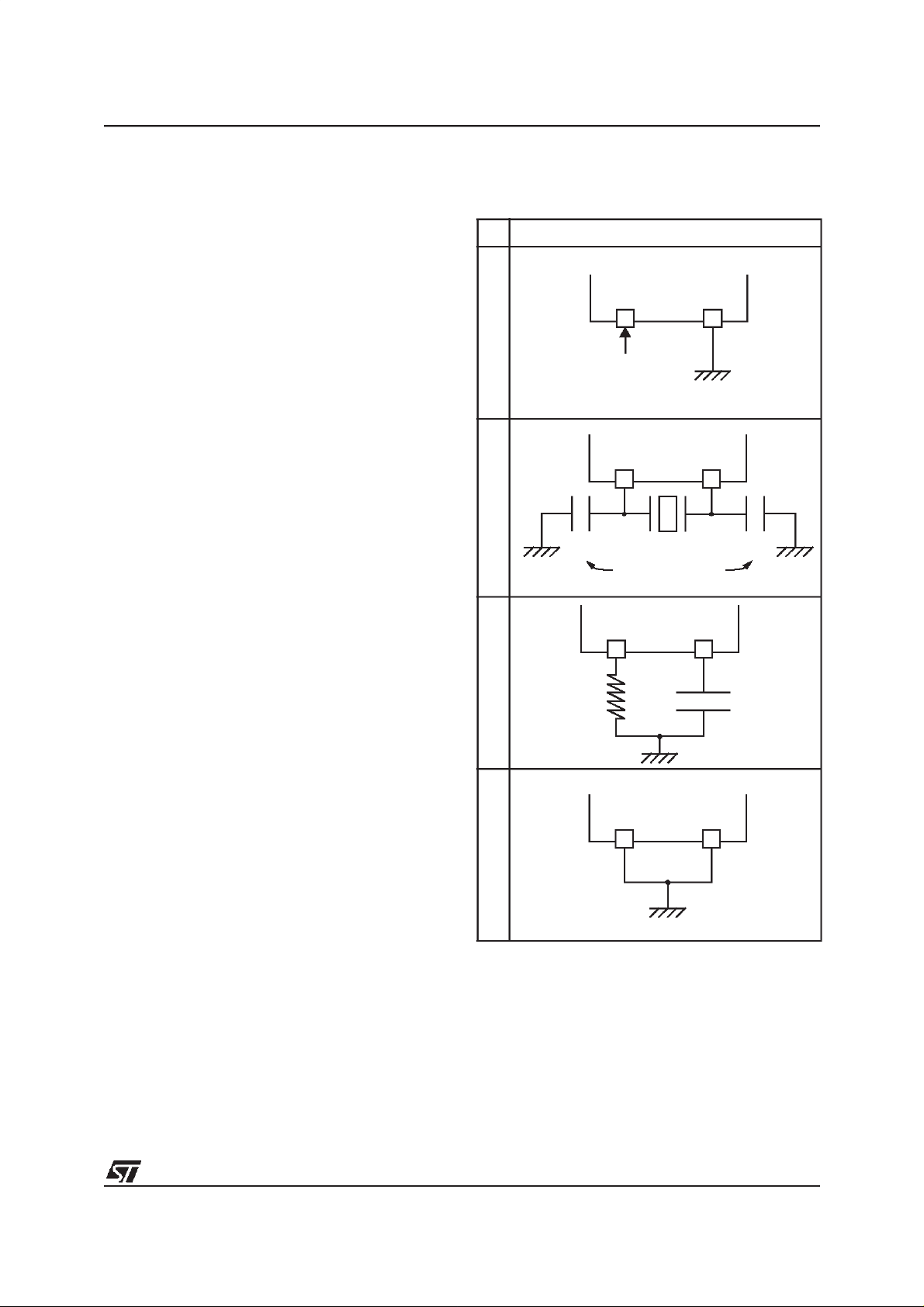
ST72104G, ST72215G, ST72216G, ST72254G
9 I/O PORTS
9.1 INTRODUCTION
The I/O ports offer different functional modes:
– transferofdatathrough digitalinputs and outputs
and for specific pins:
– external interrupt generation
– alternate signal input/output for the on-chip pe-
ripherals.
An I/O port contains up to 8 pins.Each pin can be
programmed independently as digital input(with or
without interrupt generation)or digital output.
9.2 FUNCTIONAL DESCRIPTION
Each port has 2 main registers:
– Data Register (DR)
– Data Direction Register (DDR)
and one optional register:
– Option Register (OR)
Each I/Opin may be programmed using thecorre-
sponding register bits in the DDR and OR registers: bit X corresponding to pin X of the port. The
same correspondence is used for the DR register.
The following description takes into account the
OR register, (for specific ports which do not provide this register refer to the I/O Port Implementation section). The generic I/O block diagram is
shown in Figure 21
9.2.1 Input Modes
The input configuration is selected by clearing the
corresponding DDR register bit.
In this case, reading the DR register returns the
digital value applied to the external I/O pin.
Different input modes can beselected bysoftware
through the OR register.
Notes:
1. Writing the DR register modifies the latch value
but does not affect the pin status.
2. When switching from input to output mode, the
DR register has to be written first to drive the correct level on the pin as soon as the port is configured as an output.
External interrupt function
When an I/O is configured as Input with Interrupt,
an event on this I/O can generate anexternal interrupt request to the CPU.
Each pin can independently generate an interrupt
request. The interrupt sensitivity is independently
programmable using the sensitivity bits in the Miscellaneous register.
Each external interrupt vector is linked to a dedicated group of I/O port pins (seepinout description
and interrupt section). If several input pins are selected simultaneously as interrupt source, these
are logically ANDed. For this reason if one of the
interrupt pins is tied low, it masks the other ones.
In case of a floating input with interrupt configuration, special care must be taken when changing
the configuration (see Figure 22).
The external interrupts are hardware interrupts,
which means that the request latch (not accessible
directly by the application)is automatically cleared
when the corresponding interrupt vector is
fetched. To clear an unwanted pending interrupt
by software, the sensitivity bits in the Miscellaneous register must be modified.
9.2.2 Output Modes
The output configuration is selected by setting the
corresponding DDR register bit. In this case, writing the DR register applies this digital value to the
I/O pin through the latch. Then readingthe DR register returns the previously stored value.
Two different output modes can be selected by
software through the OR register: Output push-pull
and open-drain.
DR register value and output pin status:
DR Push-pull Open-drain
0V
1V
SS
DD
Vss
Floating
9.2.3 Alternate Functions
When an on-chip peripheral is configured to use a
pin, the alternate function is automatically selected. This alternate function takes priority over the
standard I/O programming.
When the signal is coming froman on-chip peripheral, the I/O pin is automatically configured in output mode (push-pull or open drain according to the
peripheral).
When the signal is going to an on-chip peripheral,
the I/O pin must be configured in input mode. In
this case, the pin state is alsodigitally readableby
addressing theDR register.
Note: Input pull-up configuration can cause unexpected value attheinput ofthealternateperipheral
input. Whenan on-chip peripheral use a pin as input and output, this pin has to be configured in input floating mode.
30/135
 Loading...