

SGS Thomson Microelectronics ST72171K2, ST72171 Datasheet
Rev. 1.4
October 2000 1/152
This is preliminary information on a new product in development or undergoing evaluation. Details are subject to change without notice.
ST72C 171
8-BIT MCU with 8 K FLASH, ADC, WDG, SPI, SCI, TIMERS
SPGAs (Software Programmable Gain Amplifiers), OP-AMP
PRODUCT PREVIEW
■ Memories
– 8K of single voltage Flash Program memory
with read-out protection
– In-Situ Programming (Remote ISP)
■ Clock, Reset and Supply Management
– Enhanced Reset System
– Low voltage supervisor (LVD) with 3 program-
mable levels
– Low consumption resonat or or RC oscillators
(internal or external) and by-pass for external
clock source, with safe control capabilities
– 3 Power Saving modes
■ 22 I/O Ports
– 22 multifunctional bidirectional I/O lines:
– 16 interrupt inputs on 2 independent lines
– 8 lines configurable as analog inputs
– 20 alternate functions
–EMI filtering
■ 2 Timers and Watchdog
– One 16-bit Timer with: 2 Input Captures, 2
Output Compares, external Clock input, PWM
and Pulse Generator modes
– One 8-bit Autoreload Timer (ART) with: 2
PWM output channels (internally connectable
to the SPGA inputs), 1 Input Capture, external
clock input
– Configurable watchdog (WDG)
■ 2 Communications Interfaces
– Synchronous Serial Peripheral Interface (SPI)
– Serial Co m munications Int e rface (SCI)
■ 3 Analog peripherals
– 2 Software Programmable Gain Operational
Amplifie rs (SPGAs) with rail-to-rail inp ut and
output, V
DD
independent (band gap) and pro-
grammable reference voltage (1/8 V
DD
resolution), Offset compensation, DAC & on/off
switching capability
– 1 rail-to-rail input and output Op-Amp
– 8-bit A/D Converter with up to 11 channels (in-
cluding 3 internal channels connected to the
Op-Amp & SPGA outpu ts)
■ Instruction Set
– 8-bit data manipulation
– 63 basic Instructi o n s
– 17 main addressing modes
– 8 x 8 unsigned multiply instruction
– True bit manipulation
■ Development Tools
– Full hardware/software development package
Device Summary
SO34
PSDIP32
Features ST72C171K2M ST72C171K2B
Flash - bytes 8K Single Voltage
RAM (stack) - bytes 256 (128)
Peripherals
2 SPGAs, 1 Op-Amp,
Watchdog, 3 Timers, SPI, SCI, ADC (11 chan.)
2 SPGAs,
Watchdog, 3 Timers, SPI, SCI, ADC (11 chan.)
Operating Supply 3.2 V to 5.5 V
CPU Frequency Up to 8 MHz (with up to 16 MHz oscillator)
Temperature Rang e - 40°C to + 85°C
Package SO34 PSDIP32
1

Table of Contents
152
2/152
1
1 GENERAL DESCRIPTION . . . . . . . . . . . . . . . . . . . . . . . . . . . . . . . . . . . . . . . . . . . . . . . . . . . . . . 4
1.1 INTRODUCTION . . . . . . . . . . . . . . . . . . . . . . . . . . . . . . . . . . . . . . . . . . . . . . . . . . . . . . . . . 4
1.2 PIN DESCRIPTION . . . . . . . . . . . . . . . . . . . . . . . . . . . . . . . . . . . . . . . . . . . . . . . . . . . . . . . 5
1.3 MEMORY MAP . . . . . . . . . . . . . . . . . . . . . . . . . . . . . . . . . . . . . . . . . . . . . . . . . . . . . . . . . . 8
2 FLASH PROGRAM MEMORY . . . . . . . . . . . . . . . . . . . . . . . . . . . . . . . . . . . . . . . . . . . . . . . . . . 11
2.1 INTRODUCTION . . . . . . . . . . . . . . . . . . . . . . . . . . . . . . . . . . . . . . . . . . . . . . . . . . . . . . . . 11
2.2 MAIN FEATURES . . . . . . . . . . . . . . . . . . . . . . . . . . . . . . . . . . . . . . . . . . . . . . . . . . . . . . . 11
2.3 STRUCTURAL ORGANISATION . . . . . . . . . . . . . . . . . . . . . . . . . . . . . . . . . . . . . . . . . . . . 11
2.4 IN-SITU PROGRAMMING (ISP) MODE . . . . . . . . . . . . . . . . . . . . . . . . . . . . . . . . . . . . . . 11
2.5 MEMORY READ-OUT PROTECTION . . . . . . . . . . . . . . . . . . . . . . . . . . . . . . . . . . . . . . . . 11
3 CENTRAL PROCESSING UNIT . . . . . . . . . . . . . . . . . . . . . . . . . . . . . . . . . . . . . . . . . . . . . . . . . 12
3.1 INTRODUCTION . . . . . . . . . . . . . . . . . . . . . . . . . . . . . . . . . . . . . . . . . . . . . . . . . . . . . . . . 12
3.2 MAIN FEATURES . . . . . . . . . . . . . . . . . . . . . . . . . . . . . . . . . . . . . . . . . . . . . . . . . . . . . . . 12
3.3 CPU REGISTERS . . . . . . . . . . . . . . . . . . . . . . . . . . . . . . . . . . . . . . . . . . . . . . . . . . . . . . . 12
4 SUPPLY, RESET AND CLOCK MANAGEMENT . . . . . . . . . . . . . . . . . . . . . . . . . . . . . . . . . . . . 15
4.1 MAIN FEATURES . . . . . . . . . . . . . . . . . . . . . . . . . . . . . . . . . . . . . . . . . . . . . . . . . . . . . . . 15
4.2 LOW VOLTAGE DETECTOR (LVD) . . . . . . . . . . . . . . . . . . . . . . . . . . . . . . . . . . . . . . . . . 16
4.3 CLOCK SECURITY SYSTEM (CSS) . . . . . . . . . . . . . . . . . . . . . . . . . . . . . . . . . . . . . . . . . 21
4.4 CLOCK, RESET AND SUPPLY REGISTER DESCRIPTION . . . . . . . . . . . . . . . . . . . . . . 23
5 INTERRUPTS . . . . . . . . . . . . . . . . . . . . . . . . . . . . . . . . . . . . . . . . . . . . . . . . . . . . . . . . . . . . . . . 24
5.1 NON MASKABLE SOFTWARE INTERRUPT . . . . . . . . . . . . . . . . . . . . . . . . . . . . . . . . . . 24
5.2 EXTERNAL INTERRUPTS . . . . . . . . . . . . . . . . . . . . . . . . . . . . . . . . . . . . . . . . . . . . . . . . 24
5.3 PERIPHERAL INTERRUPTS . . . . . . . . . . . . . . . . . . . . . . . . . . . . . . . . . . . . . . . . . . . . . . . 24
6 POWER SAVING MODES . . . . . . . . . . . . . . . . . . . . . . . . . . . . . . . . . . . . . . . . . . . . . . . . . . . . . 27
6.1 INTRODUCTION . . . . . . . . . . . . . . . . . . . . . . . . . . . . . . . . . . . . . . . . . . . . . . . . . . . . . . . . 27
6.2 SLOW MODE . . . . . . . . . . . . . . . . . . . . . . . . . . . . . . . . . . . . . . . . . . . . . . . . . . . . . . . . . . . 27
6.3 WAIT MODE . . . . . . . . . . . . . . . . . . . . . . . . . . . . . . . . . . . . . . . . . . . . . . . . . . . . . . . . . . . 28
6.4 HALT MODE . . . . . . . . . . . . . . . . . . . . . . . . . . . . . . . . . . . . . . . . . . . . . . . . . . . . . . . . . . . 29
7 ON-CHIP PERIPHERALS . . . . . . . . . . . . . . . . . . . . . . . . . . . . . . . . . . . . . . . . . . . . . . . . . . . . . . 30
7.1 I/O PORTS . . . . . . . . . . . . . . . . . . . . . . . . . . . . . . . . . . . . . . . . . . . . . . . . . . . . . . . . . . . . . 30
7.2 MISCELLANEOUS REGISTERS . . . . . . . . . . . . . . . . . . . . . . . . . . . . . . . . . . . . . . . . . . . . 36
7.3 OP-AMP MODULE . . . . . . . . . . . . . . . . . . . . . . . . . . . . . . . . . . . . . . . . . . . . . . . . . . . . . . . 38
7.4 WATCHDOG TIMER (WDG) . . . . . . . . . . . . . . . . . . . . . . . . . . . . . . . . . . . . . . . . . . . . . . . 48
7.5 16-BIT TIMER . . . . . . . . . . . . . . . . . . . . . . . . . . . . . . . . . . . . . . . . . . . . . . . . . . . . . . . . . . 51
7.6 PWM AUTO-RELOAD TIMER (ART) . . . . . . . . . . . . . . . . . . . . . . . . . . . . . . . . . . . . . . . . . 69
7.7 SERIAL COMMUNICATIONS INTERFACE (SCI) . . . . . . . . . . . . . . . . . . . . . . . . . . . . . . . 78
7.8 SERIAL PERIPHERAL INTERFACE (SPI) . . . . . . . . . . . . . . . . . . . . . . . . . . . . . . . . . . . . 89
7.9 8-BIT A/D CONVERTER (ADC) . . . . . . . . . . . . . . . . . . . . . . . . . . . . . . . . . . . . . . . . . . . . 102
8 INSTRUCTION SET . . . . . . . . . . . . . . . . . . . . . . . . . . . . . . . . . . . . . . . . . . . . . . . . . . . . . . . . . 106
8.1 ST7 ADDRESSING MODES . . . . . . . . . . . . . . . . . . . . . . . . . . . . . . . . . . . . . . . . . . . . . . 106
8.2 INSTRUCTION GROUPS . . . . . . . . . . . . . . . . . . . . . . . . . . . . . . . . . . . . . . . . . . . . . . . . 109

Table of Contents
3/152
9 ELECTRICAL CHARACTERISTICS . . . . . . . . . . . . . . . . . . . . . . . . . . . . . . . . . . . . . . . . . . . . . 112
9.1 PARAMETER CONDITIONS . . . . . . . . . . . . . . . . . . . . . . . . . . . . . . . . . . . . . . . . . . . . . . 112
9.2 ABSOLUTE MAXIMUM RATINGS . . . . . . . . . . . . . . . . . . . . . . . . . . . . . . . . . . . . . . . . . . 113
9.3 OPERATING CONDITIONS . . . . . . . . . . . . . . . . . . . . . . . . . . . . . . . . . . . . . . . . . . . . . . . 114
9.4 SUPPLY CURRENT CHARACTERISTICS . . . . . . . . . . . . . . . . . . . . . . . . . . . . . . . . . . . 116
9.5 CLOCK AND TIMING CHARACTERISTICS . . . . . . . . . . . . . . . . . . . . . . . . . . . . . . . . . . 119
9.6 MEMORY CHARACTERISTICS . . . . . . . . . . . . . . . . . . . . . . . . . . . . . . . . . . . . . . . . . . . 123
9.7 EMC CHARACTERISTICS . . . . . . . . . . . . . . . . . . . . . . . . . . . . . . . . . . . . . . . . . . . . . . . 124
9.8 I/O PORT PIN CHARACTERISTICS . . . . . . . . . . . . . . . . . . . . . . . . . . . . . . . . . . . . . . . . 129
9.9 CONTROL PIN CHARACTERISTICS . . . . . . . . . . . . . . . . . . . . . . . . . . . . . . . . . . . . . . . 132
9.10TIMER PERIPHERAL CHARACTERISTICS . . . . . . . . . . . . . . . . . . . . . . . . . . . . . . . . . . 135
9.11COMMUNICATION INTERFACE CHARACTERISTICS . . . . . . . . . . . . . . . . . . . . . . . . . 136
9.128-BIT ADC CHARACTERISTICS . . . . . . . . . . . . . . . . . . . . . . . . . . . . . . . . . . . . . . . . . . . 139
9.13OP-AMP MODULE CHARACTERISTICS . . . . . . . . . . . . . . . . . . . . . . . . . . . . . . . . . . . . 141
10 GENERAL INFORMATION . . . . . . . . . . . . . . . . . . . . . . . . . . . . . . . . . . . . . . . . . . . . . . . . . . . 144
10.1PACKAGE MECHANICAL DATA . . . . . . . . . . . . . . . . . . . . . . . . . . . . . . . . . . . . . . . . . . . 144
10.2THERMAL CHARACTERISTICS . . . . . . . . . . . . . . . . . . . . . . . . . . . . . . . . . . . . . . . . . . 145
10.3SOLDERING AND GLUEABILITY INFORMATION . . . . . . . . . . . . . . . . . . . . . . . . . . . . . 146
10.4PACKAGE/SOCKET FOOTPRINT PROPOSAL . . . . . . . . . . . . . . . . . . . . . . . . . . . . . . . 146
11 DEVICE CONFIGURATION AND ORDERING INFORMATION . . . . . . . . . . . . . . . . . . . . . . . 147
11.1OPTION BYTES . . . . . . . . . . . . . . . . . . . . . . . . . . . . . . . . . . . . . . . . . . . . . . . . . . . . . . . . 147
11.2DEVICE ORDERING INFORMATION . . . . . . . . . . . . . . . . . . . . . . . . . . . . . . . . . . . . . . . 148
11.3DEVELOPMENT TOOLS . . . . . . . . . . . . . . . . . . . . . . . . . . . . . . . . . . . . . . . . . . . . . . . . . 149
11.4ST7 APPLICATION NOTES . . . . . . . . . . . . . . . . . . . . . . . . . . . . . . . . . . . . . . . . . . . . . . 150
11.5TO GET MORE INFORMATION . . . . . . . . . . . . . . . . . . . . . . . . . . . . . . . . . . . . . . . . . . . 150
12 SUMMARY OF CHANGES . . . . . . . . . . . . . . . . . . . . . . . . . . . . . . . . . . . . . . . . . . . . . . . . . . . 151
ST72C171
4/152
1 GENERAL DESCRIPTION
1.1 INTRODUCTION
The ST72C171 is a member of the ST7 family of
Microcontrollers. All devices are based on a com mon industry-standard 8-bit core, featuring an enhanced instruction set.
The ST72C171 features single-voltage FLASH
memory with byte-by-byte In-Situ Programming
(ISP) capability.
Under software control, the device can be placed
in WAIT, SLOW, or HALT mode, reducing po wer
consumption when the application is in idle or
standby state.
The enhanced instruction set and addressing
modes of the ST7 offer both power and flexibility to
software developers, enabling the design of highly
efficient and compact application code. In addition
to standard 8-bit data management, all ST7 microcontrollers feature true bit manipulation, 8x8 un-
signed multiplication and indirect addressing
modes The device includes a low consumption
and fast start on-chip oscillator, CPU, Flash program memory, RAM, 22 I/O lines and the following
on-chip peripherals: Analog-to-Digital converter
(ADC) with 8 multiplexed a nalog inputs, Op-Amp
module, synchronous SPI serial interface, asyncronous serial interface (SCI), Watchdog timer, a
16-bit Timer featuring external Clock I nput, Pulse
Generator capabilities, 2 Input Captures and 2
Output Compares, an 8-bit Timer featuring external Clock Input, Pulse Generator Capabilities (2
channels), Autoreload and Input Capture.
The Op-Amp module adds on-chip analog features to the MCU, that usually require using external components.
Figure 1. ST72C171 Block Diagram
ADDRESS AND DATA BUS
OSCIN
OSCOUT
RESET
16-BIT TIMER
8-BIT ADC
PORT B
WATCHDOG
Internal
CLOCK
CONTROL
256b-RAM
PA[7:0]
V
SS
V
DD
POWER
SUPPLY
8K FLASH
PORT A
PWM/ART TIMER
SPI
PB[7:0]
LVD
SCI
MULTIOSC
+
CLOCK FILTER
OP-AMP
V
SSA
V
DDA
8-BIT CORE
ALU
PORT C
PC[5:0]
OA1OUT
OA2OUT
MEMORY
OA3OUT*
*only on 34-pin devices
OA3PIN*
ST72C171
5/152
1.2 PIN DESCRI PTION
Figure 2. 34-Pin SO Package Pinout
Figure 3. 32-Pin SDIP Package Pinout
PC2 / OA1PIN / PWM0R
PC3 / OA1NIN
OA1OUT
PC4 / MCO/ OA3NIN
V
DDA
V
SSA
OA3OUT
PC5/ PWM0
PA7 / AIN7 / PWM1
PA6 / AIN6 / ARTICP0
PA5 / A IN5
PA4 / AIN4 / OCMP1
PA3 / AIN3 / OCMP2
PA2 / AIN2 / ICAP1
PA1 / AIN1 / ICAP2
PA0 / A IN0
RESET
21
22
23
24
25
26
34
33
32
31
30
29
28
27
1
2
3
4
5
6
7
8
9
10
11
12
13
14
OA2OUT
PWM1R / OA2PIN / PC1
OA2NIN / PC0
OA3PIN
TDO / PB7
RDI / PB6
ISPDATA / MISO / PB5
MOSI /
(HS)
PB4
ISPCLK / SCK /
(HS)
PB3
SS
/
(HS)
PB2
ARTCLK /
(HS)
PB1
EXTCLK /
(HS)
PB0
V
DD
V
SS
OSC2
OSC1
ISPSEL
15
16
17
20
19
18
ei1
ei0
(HS)
20mA high sink capability
OA2OUT
PWM1R / OA2PIN / PC1
OA2N IN / PC0
TDO / PB7
RDI / PB6
ISPDATA / MISO / PB5
MOSI /
(HS)
PB4
ISPCLK / SCK/
(HS)
PB3
SS
/
(HS)
PB2
ARTCLK /
(HS)
PB1
EXTCLK /
(HS)
PB0
V
DD
V
SS
OSC2
OSC1
ISPSEL
PC2 / OA1PIN / PWM0R
PC3 / OA1NIN
OA1OUT
PC4 / MCO
V
DDA
V
SSA
PC5 / PWM0
PA7 / AIN7 / PWM1
PA6 / AIN6 /ARTICP0
PA5 / AIN5
PA4 / AIN4 / OCMP1
PA3 / AIN3 / OCMP2
PA2 / AIN2 / ICAP1
PA1 / AIN1 / ICAP2
PA0 / AIN0
RESET
1
2
3
4
5
6
7
8
9
10
11
12
13
14
15
16
32
31
30
29
28
27
26
25
24
23
22
21
20
19
18
17
ei1
ei0
(HS)
20mA high sink capability
ST72C171
6/152
PIN DESCRIPTION (Cont’d)
Legend / Abbreviations:
Type: I = input, O = output, S = supply
In/Output level: C = CMOS 0.3V
DD
/0.7VDD,
C
R
= CMOS Levels with resistive output (1K)
A = Analog levels
Output level: HS = high sink (on N-buffer only),
Port configuration capabilities:
– Input:float = floating, wpu = weak pull-up, int = interrupt, ana = analog
– Output: OD = open drain, T = true open drain, PP = push-pull
Note: the Reset configuration of each pin is shown in bold.
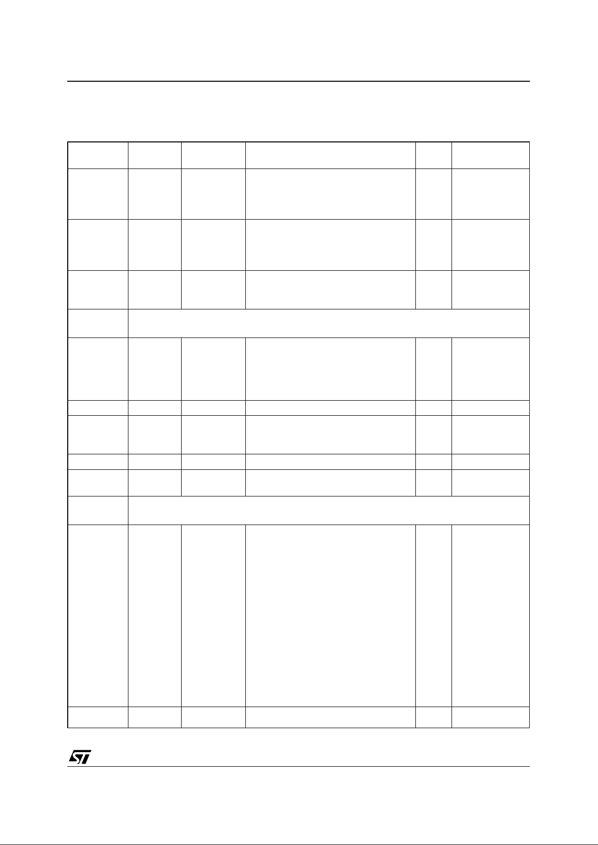
Table 1. Device Pin Description
Pin
n°
Pin Name
Type
Level Port
Main
function
(after
reset)
Alternate function
SDIP32
SO34
Input
Output
Input Output
float
wpu
int
ana
OD
PP
1 1 OA2OUT O A OA2 output
22
PC1/OA2PIN/
PWM1R
I/O C C/C
R
X X X X X Port C1
OA2 noninverting input and/o r
ART PWM1 resistive output
3 3 PC0/OA2NIN I/O C/A C X X X X X Port C0 OA2 inverting input
- 4 OA3PIN I A OA3 noninverting input
4 5 PB7/TDO I/O C X ei1 X X Port B7 SCI transmit
5 6 PB6/RDI I/O C X ei1 X X Port B6 SCI receive
6 7 PB5/MISO/ISPDATA I/O C X ei1 X X Port B5
SPI data master in/slave out or
In Situ Programming Data Input
7 8 PB4/MOSI I/O C HS X ei1 X X Port B4 SPI data master out/slave in
8 9 PB3/SCK/ISPCLK I/O C HS X ei1 X X Port B3
SPI Clock or In Situ Programming Clock Output
910PB2/SS
I/O C HS X ei1 X X Port B2 SPI Slave Select (active low)
10 11 PB1/ARTCLK I/O C HS X ei1 X X Port B1 ART External Clock
11 12 PB0/EXTCLK I/O C HS X ei1 X X Port B0 Timer16 External Clock
12 13 V
DD
S Digital Main Supply Voltage
13 14 V
SS
S Digital ground voltage
14 15 OSC2
Resonator oscillator inverter output or capacitor input for RC oscillator
15 16 OSC1
External clock input or Resonator oscillator inverter input or resistor input for RC oscillator
16 17 ISPSEL I C
In Situ Programming Mode Select
Must be tied to V
SS
in user mode
17 18 RESET
I/O C X X External Reset
18 19 PA 0/AIN 0 I/O C X ei0 X X X Port A0 ADC input 0
19 20 PA1/AIN1/ICAP2 I/O C X ei0 X X X Port A1
ADC input 1 orTimer16 input
capture 2
ST72C171
7/152
Notes:
1. In the interrupt input column, “eix” define s the associated external interrupt vect or. If the weak pull-up
column (wpu) is associated with the interrupt column (int), then the I/O configuration is p ull-up interrupt
input, else the configuration is floating interrupt input.
2. OSC1 and OSC2 pins connect a crystal or ceramic resonator, an external RC, or an external source to
the on-chip oscillator see dedicated See “PIN DESCRIPTION” on page 5. for more details.
20 21 PA2/AIN2/ICAP1 I/O C X ei0 X X X Port A2
ADC input 2
or Timer16 input capture 1
21 22 PA3/AIN3/OCMP2 I/O C X ei0 X X X Port A3
ADC input 3 or Timer16 output
compare 2
22 23 PA4 /AIN4/OCMP1 I/O C X ei0 X X X Port A4
ADC input 4 or Timer16 output
compare 1
23 24 PA5/AIN5 I/O C X ei0 X X X Port A5 ADC input 5
24 25 PA6/AIN6/ARTICP0 I/O C X ei0 X X X Port A6
ADC input 6 or ART input capture
25 26 PA7/AIN7/PWM1 I/O C X ei0 X X X Port A7
ADC input 7 or ART PWM1
output
26 27 PC 5 / P W M0 I/O C X X X X Port C5 ART PWM0 output
- 28 OA3OUT O A OA3 output
27 29 V
SSA
Analog ground
28 30 V
DDA
Analog supply
29 31 PC4/MCO/OA 3NIN I/O C X X X X Port C4
Main Clock Out or OA3 invert-
ing input
30 32 OA1OUT O A OA1 output
31 33 PC3/OA1NIN I/O C/A C X X X X Port C3 OA1 inverting input
32 34
PC2/OA1PIN/
PWM0R
I/O C/A C/C
R
X X X X Port C2
OA1 non-inverting input and/
or ART PWM0 resistive output
Pin
n°
Pin Name
Type
Level Port
Main
function
(after
reset)
Alternate function
SDIP32
SO34
Input
Output
Input Output
float
wpu
int
ana
OD
PP
ST72C171
8/152
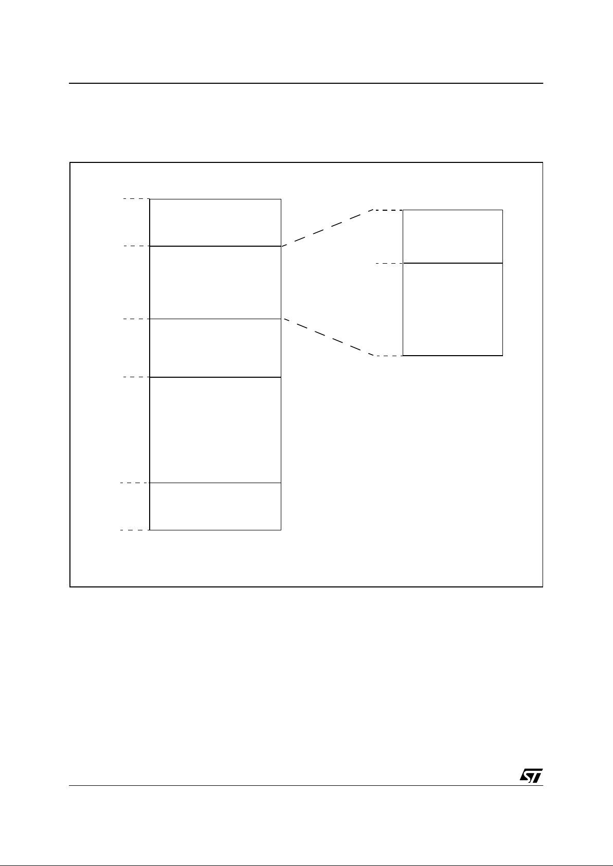
1.3 MEMORY MA P
1.3.1 Introd uct i on
Figure 4. Program Memory M ap
Short Addressing
RAM
Stack
0100h
017Fh
0080h
00FFh
0000h
8 Kbytes
Interrupt & Reset Vectors
HW Registers
017Fh
0080h
007Fh
0180h
DFFFh
Reserved
(see Table 1.3.2)
E000h
FFDFh
FFE0h
FFFFh
(see Table 4)
256 bytes RAM
FLASH
(128 Bytes)
(128 Bytes)
Zero page
ST72C171
9/152
1.3.2 Data Register
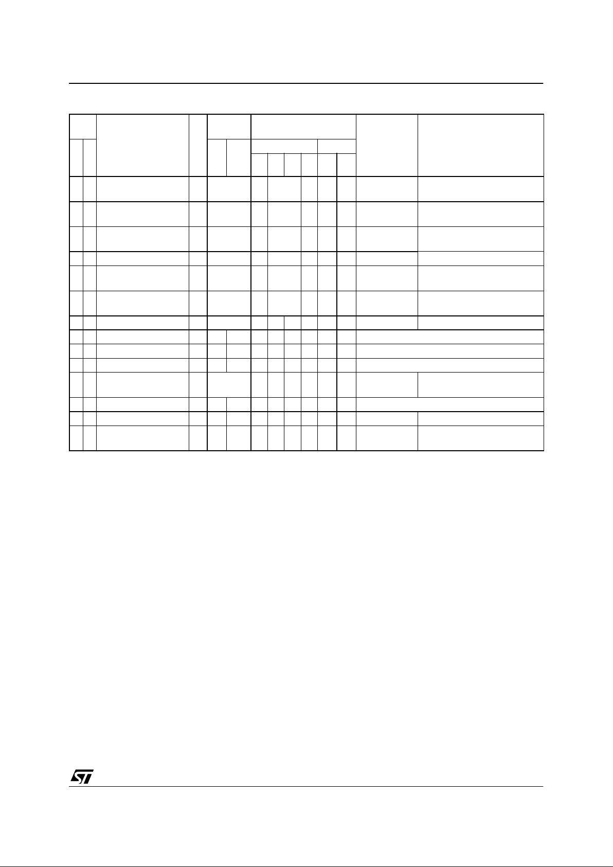
Table 2. Hardware Register Mem ory Map
Address
Block
Name
Register
Label
Register name
Reset
Status
Remarks
0000h
0001h
0002h
0003h
Port A
PADR
PADDR
PAOR
Data Register
Data Direction Register
Option Register
Not Used
00h
00h
00h
R/W
R/W
R/W
Absent
0004h
0005h
0006h
0007h
Port B
PBDR
PBDDR
PBOR
Data Register
Data Direction Register
Option Register
Not Used
00h
00h
00h
R/W
R/W
R/W
Absent
0008h
0009h
000Ah
Port C
PCDR
PCDDR
PCOR
Data Register
Data Direction Register
Option Register
00h
00h
00h
R/W
R/W
R/W
000Bh to
001Ah
Reserved Area (16 Bytes)
001Bh
001Ch
001Dh
001Eh
001Fh
OPAMP
OA1CR
OA2CR
OA3CR
OAIRR
OAVRCR
OA1 Control Register
OA2 Control Register
OA3 Control Register
OA Interrupt & Readout Register
OA Voltage Reference Control Register
00h
00h
00h
00h
00h
R/W
R/W
R/W
Section 7.3
R/W
0020h MISC1 MISCR1 Miscellaneous Register 1 00h see Section 4.3.5
0021h
0022h
0023h
SPI
SPIDR
SPICR
SPISR
Data I/O Register
Control Register
Status Register
xxh
0xh
00h
R/W
R/W
Read Only
0024h WDG WDGCR Watchdog Control register 7Fh R/W
0025h CRS CRSR
Clock, Reset and Supply Control / Status
Register
00h R/W
0026h to
0030h
Reserved Area (11 Bytes)
0031h
0032h
0033h
0034h0035h
0036h0037h
0038h0039h
003Ah003Bh
003Ch003Dh
003Eh003Fh
TIMER16
TACR2
TACR1
TASR
TAIC1HR
TAIC1LR
TAOC1HR
TAOC1LR
TACHR
TACLR
TAACHR
TAACLR
TAIC2HR
TAIC2LR
TAOC2HR
TAOC2LR
Control Register2
Control Register1
Status Register
Input Capture1 High Register
Input Capture1 Low Register
Output Compare1 High Register
Output Compare1 Low Register
Counter High Register
Counter Low Register
Alternate Counter High Register
Alternate Counter Low Register
Input Capture2 High Register
Input Capture2 Low Register
Output Compare2 High Register
Output Compare2 Low Register
00h
00h
xxh
xxh
xxh
80h
00h
FFh
FCh
FFh
FCh
xxh
xxh
80h
00h
R/W
R/W
Read Only
Read Only
Read Only
R/W
R/W
Read Only
Read Only
Read Only
Read Only
Read Only
Read Only
R/W
R/W
0040h MISC2 MISCR2 Miscellaneous Register2 00h see Section 7.2.2
ST72C171
10/152
0041h to
004Fh
Reserved Area (15 Bytes)
0050h
0051h
0052h
0053h
0054h
SCI
SCISR
SCIDR
SCIBRR
SCICR1
SCICR2
Status Register
Data Register
Baud Rate Register
Control Register 1
Control Register 2
0C0h
0xxh
0Xxh
0xxh
00h
Read Only
R/W
R/W
R/W
R/W
0055h to
006Fh
Reserved Area (27 Bytes)
0070h
0071h
ADC
ADCDR
ADCCSR
Data Register
Control/Status Register
00h
00h
Read Only
R/W
0072h
0073h
Reserved Area (2 Bytes)
0074h
0075h
0076h
0077h
0078h
0079h
007Ah
007Bh
ART/PWM
PWMDCR1
PWMDCR0
PWMCR
ARTCSR
ARTCAR
ARTARR
ARTICCSR
ARTICR1
PWM Duty Cycle Register 1
PWM Duty Cycle Register 0
PWM Control Register
Control/Status Register
Counter Access Register
Auto Reload Register
Input Capture Control Status Register
Input Capture Register 1
00h
00h
00h
00h
00h
00h
00h
R/W
R/W
R/W
R/W
R/W
R/W
R/W
Read Only
007Ch to
007Fh
Reserved Area (4 Bytes)
Address
Block
Name
Register
Label
Register name
Reset
Status
Remarks
ST72C171
11/152
2 FLASH PROGRAM MEMORY
2.1 INTRODUCTION
FLASH devices have a single voltage non-volatil e
FLASH memory that may be programmed in-situ
(or plugged in a programming t ool) on a byte-bybyte basis.
2.2 MAIN FEATURES
■ Remote In-Situ Programming (ISP) mode
■ Up to 16 bytes programmed in the same cycle
■ MTP memory (Multiple Time Programmable)
■ Read-out memory protection against piracy
2.3 STRUCTURAL ORGANISATION
The FLASH program memory is organised in a
single 8-bit wide memory block which can be used
for storing both code and data constants.
The FLASH program memory is mapped in the upper part of the ST7 addressing space and includes
the reset and interrupt user vector area .
2.4 IN-SITU PROGRAMMING (ISP) MODE
The FLASH program memory can be programmed
using Remote ISP mode. This ISP mode allows
the contents of the ST7 program memory to be updated using a standard ST7 programming tools after the device is mounted on the application board.
This feature can be implem ented with a m inimum
number of added componen ts and bo ard area impact.
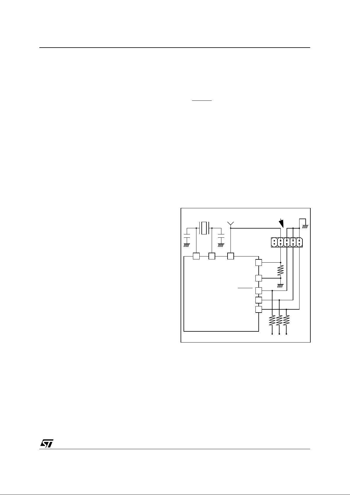
An example Remote ISP hardware interface to t he
standard ST7 programmi ng tool is described below. For more details on ISP programming, refer to
the ST7 Programming Specification.
Remote ISP Overview
The Remote ISP mode is initiated by a specific sequence on the dedicated ISPSEL pin.
The Remote ISP is performed in three steps:
– Selection of the RAM execution mode
– D ownl oad of Remote ISP code in RAM
– Execution of Remote ISP code in RAM to pro-
gram the user program into the FLASH
Remote ISP hardware configuration
In Remote ISP mode, the ST7 has to be supplied
with power (V
DD
and VSS) and a clock signal (os-
cillator and application crystal circuit for example).
This mode needs five signals (plus the V
DD
signal
if necessary) to be connected to the program m ing
tool. This signals are:
– RESET
: device reset
–V
SS
: device ground power supply
– I S PCLK: ISP output serial clock pin
– ISPDATA: ISP input serial data pin
– ISPSEL: Remote ISP mode selection. This pin
must be connected to V
SS
on the application
board through a pull-down resistor.
If any of these pins are used for other purposes on
the application, a serial resist or has to be implemented to avoid a conflict if the other device forces
the signal level.
Figure 1 shows a typical hardware interface to a
standard ST7 programming t ool. For more det ails
on the pin locations, refer t o t he d ev ice pin out description.
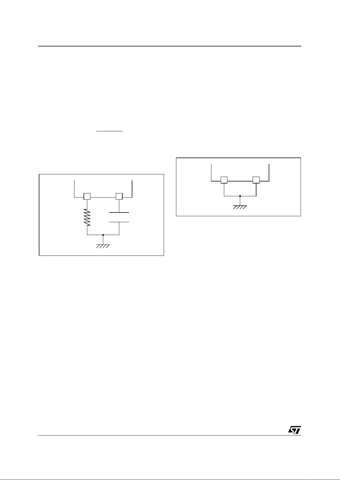
Figure 5. Typi ca l Remote ISP Inter fa ce
2.5 MEMORY READ-OUT PROTECTION
The read-out protection is enabled throug h an option bit.
For FLASH devices, when this option is selected,
the program and data stored in the FLASH memory are protected against read-out piracy (including
a re-write protection). When this protection opt ion
is removed the entire FLASH program memory is
first automatically erased. However, the E
2
PROM
data memory (when available) can be protected
only with ROM devices.
ISPSEL
V
SS
RESET
ISPCLK
ISPDATA
OSC1
OSC2
V
DD
ST7
HE10 CONNECTOR TYPE
TO PROGRAMMING TOOL
10KΩ
C
L0
C
L1
APPLICATION
47KΩ
1
XTAL
ST72C171
12/152
3 CENTRAL PROCE SSI NG UNIT
3.1 INTRODUCTION
This CPU has a full 8-bit architecture and contains
six internal registers allowing efficient 8-bit data
manipulation.
3.2 MAIN FEATURES
■ 63 basic instructions
■ Fast 8-bit by 8-bit multiply
■ 17 main addressing modes
■ Two 8-bit index registers
■ 16-bit stack pointer
■ Low po wer mo des
■ Maskable hardware interrupts
■ Non-maskable software interrupt
3.3 CPU REGISTERS
The 6 CPU registers shown in Figure 1 are not
present in the memory mapping and are accessed
by specific instructions.
Accumulator (A)
The Accumulator is an 8-bit general purpose register used to hold operan ds and the results of the
arithmetic and logic calculations and to manipulate
data.
Index Registers (X and Y)
In indexed addressing modes, these 8-bit registers
are used to create either effective addresses or
temporary storage areas for data manipulation.
(The Cross-Assembler generates a precede instruction (PRE) to indicate that the following instruction refers to the Y register.)
The Y register is not affected by the interrupt automatic procedures (not pushed to and popped from
the stack).
Program Cou nt er (P C )
The program counter is a 16-bit register containing
the address of the next instruction to be executed
by the CPU. It is made of two 8-bit registers PCL
(Program Counter Low which is the LSB) and PCH
(Program Counter High which is the MSB).
Figure 6. CPU Registers
ACCUMULA T OR
X INDEX REGISTER
Y INDEX REGISTER
STACK POINTER
CONDITION CODE REGISTER
PROGRAM COUNTER
70
1C11HI NZ
RESET VALUE = RESET VECTOR @ FFFEh-FFFFh
70
70
70
0
7
15 8
PCH
PCL
15
8
70
RESET VALUE = STACK HIGHER ADDRESS
RESET VALUE =
1X11X1XX
RESET VALUE = XXh
RESET VALUE = XXh
RESET VALUE = XXh
X = Undefined Value

ST72C171
13/152
CPU REGISTERS (Cont’d)
CONDITION CODE REGISTER (CC)
Read/Write
Reset Value: 111x1xxx
The 8-bit Condition Code register c ontains the interrupt mask and four flags represent ative of the
result of the instruction just executed. This register
can also be handled by the PUSH and POP instructions.
These bits can be individually tested and/or controlled by specific instructions.
Bit 4 = H
Half carry
.
This bit is set by hardware when a carry occurs between bits 3 and 4 of t he ALU during an ADD or
ADC instruction. It is reset by hardware during the
same instructions.
0: No half carry has occurred.
1: A half carry has occurred.
This bit is tested using the JRH or JRNH instruction. The H bit is useful in BCD arithmetic subroutines .
Bit 3 = I
Interrupt mask
.
This bit is set by hardware when entering in interrupt or by software to disable all interrup ts except
the TRAP software interrupt. This bit is cleared by
software.
0: Interrupts are enabled.
1: Interrupts are disabled.
This bit is controlled by the RIM, SIM and IRET instructions and is tested by the JRM and JRNM instructions.
Note: Interrupts requested while I is set are
latched and can be processed whe n I is cleared.
By default an interrupt routine is not in terruptable
because the I bi t is set by hardware at the start of
the routine and reset by the IRET instruction at the
end of the routine. If the I bit is cleared by software
in the interrupt routine, pending interrupts are
serviced regardless of the priority level of the current interrupt routine.
Bit 2 = N
Negative
.
This bit is set and cleared by hardware. It is representative of the result sign of the last arithmeti c,
logical or data manipulation. It is a copy of the 7
th
bit of the result.
0: The result of the last operation is positive or null.
1: The result of the last operation is negative
(i.e. the most significant bit is a logic 1).
This bit is accessed by the JRMI and JRPL instructions.
Bit 1 = Z
Zero
.
This bit is set and cleared by hardware. This bit indicates that the result of the last arithmetic, logical
or data manipulation is zero.
0: The result of the last operation is different from
zero.
1: The result of the last operation is zero.
This bit is accessed by the JREQ and JRNE test
instructions.
Bit 0 = C
Carry/borrow.
This bit is set and cleared b y hardware and software. It indicates an overflow or an underflow has
occurred during the last arithmetic operation.
0: No overflow or underflow has occurred.
1: An overflow or underflow has occurred.
This bit is driven by the SCF and RCF instructions
and tested by the JRC and JRNC instructions. It is
also affected by the “bit test and branch”, shift and
rotate instructions.
70
111HINZC
ST72C171
14/152
CENTRAL PROCESSING UNIT (Cont’d)
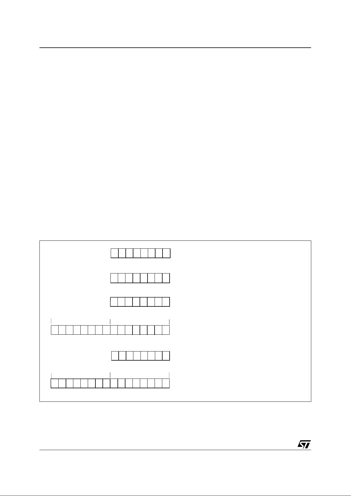
Stack Pointer (SP)
Read/Write
Reset Value: 01 7Fh
The Stack Pointer is a 16-bit register which is always pointing to the next free location in the stack.
It is then decremented after data has been pushed
onto the stack and incremented before data is
popped from the stack (see Figure 7).
Since the stack is 128 bytes deep, the 10 most significant bits are forced by hardw are. Following a n
MCU Reset, or after a Reset Stack Pointe r instruction (RSP), the Stack Pointer contains its reset value (the SP5 to SP0 bits are set) which is the stack
higher address.
The least significant byte of the Stack Pointer
(called S) can be directly accessed by a LD instruction.
Note: When the lower limit is exceeded, the Stack
Pointer wraps around to the stack upper limit, wi thout indicating the s tack overflow. The previously
stored information is then o verwritten and therefore lost. The stack also wraps in case of an underflow.
The stack is used to save the retu rn address during a subroutine call and the CPU context during
an interrupt. The user may also directly manipulate
the stack by means of the PUSH and POP instructions. In the case of an interrupt, the PCL is stored
at the first location point ed to by the SP. Then the
other registers are stored in the next locations as
shown in Figure 7.
– When an interrupt is received, the SP is decre-
mented and the context is pushed on the stack.
– On return from interrupt, the SP is incremented
and the context is popped from the stack.
A subroutine call occupies two locations and an interrupt five locat ions i n the sta ck ar ea.
Figure 7. Stack Manipulation Example
15 8
00000001
70
0 1 SP5 SP4 SP3 SP2 SP1 SP0
PCH
PCL
SP
PCH
PCL
SP
PCL
PCH
X
A
CC
PCH
PCL
SP
PCL
PCH
X
A
CC
PCH
PCL
SP
PCL
PCH
X
A
CC
PCH
PCL
SP
SP
Y
CALL
Subroutine
Interrupt
Event
PUSH Y POP Y IRET
RET
or RSP
@ 017Fh
@ 0100h
Stack Higher Address = 017Fh
Stack Lower Address =
0100h
ST72C171
15/152
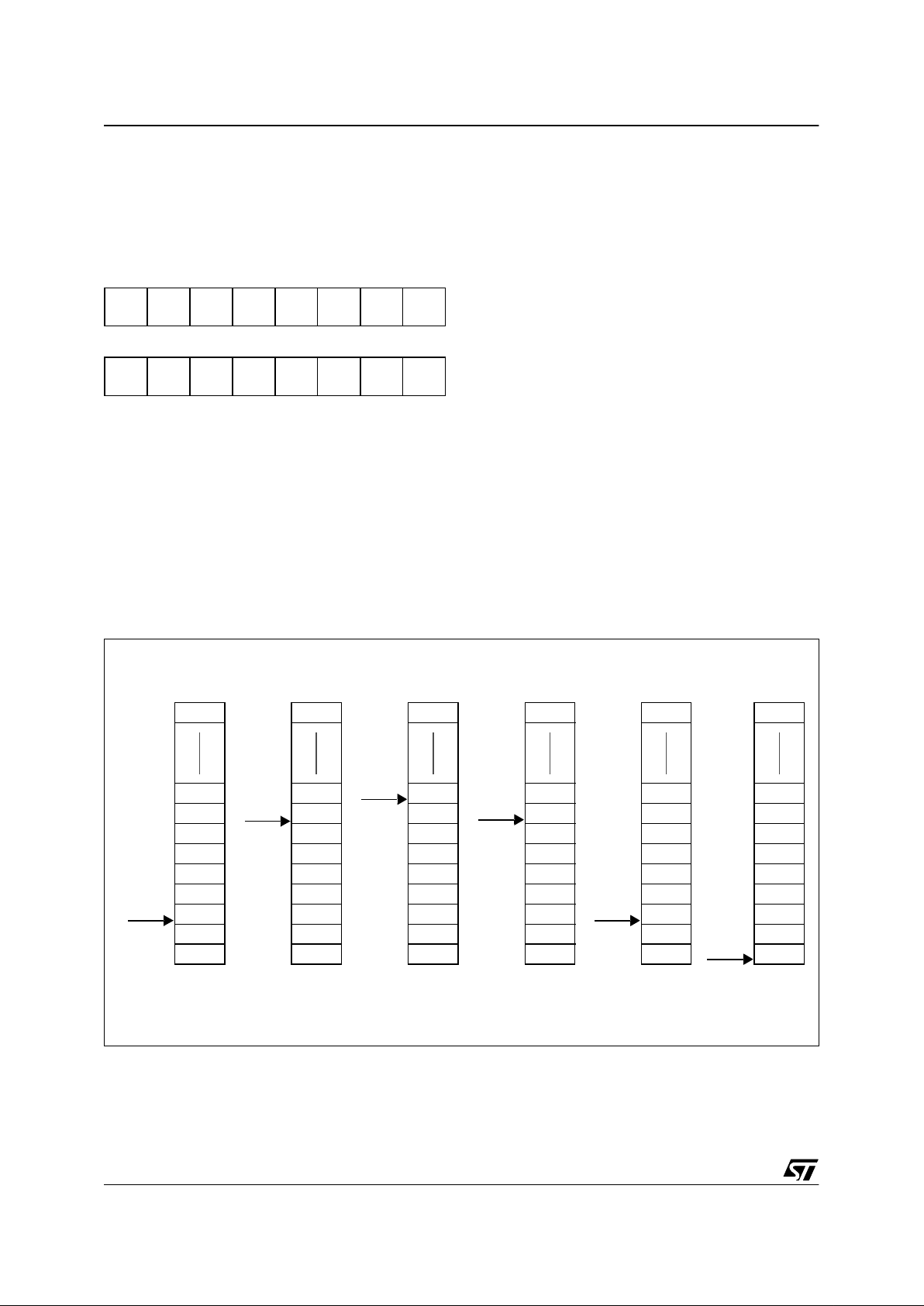
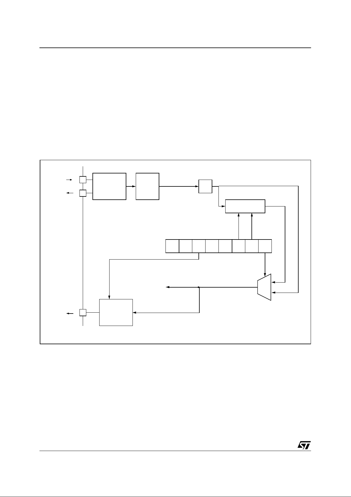
4 SUPPLY, RES ET AND CLOCK
MANAGEMENT
The device includes a range of utility features for
securing the application in critical situations (for
example in case of a power brown-out), and reducing the number of external components. An
overview is shown in Figure 8.
4.1 Main Features
■ Supply Manager
– Main supply Low voltage detection (LVD)
– Global power down
■ Reset Sequence Manager (RSM)
■ Multi-Oscillat o r (MO)
– 4 Cry stal/Ceramic res onator oscillators
– 2 External RC oscillators
– 1 Internal RC oscillator
■ Clock Security System (CSS)
–Clock Filter
– Backup Safe Oscillator
■ Main Clock controller (MCC)
Figure 8. Clock, Reset and Supply Block Diagram
IE SOD0- - - RF RF
CRSR
CSS- WDG
f
OSC
MAIN CLOCK
CONTROLLER
(MCC)
CF INTERRUPT
LVD
LOW VOL T AG E
DETECTOR
(LVD)
MULTI-
OSCILLATOR
(MO)
f
CPU
FROM
WATCHDOG
PERIPH ER AL
MCO
OSCOUT
OSCIN
RESET
V
DD
V
SS
RESETSEQUENCE
MANAGER
(RSM)
CLOCK
FILTER
SAFE
OSC
CLOCKSECURITYSYSTEM
(CSS)
ST72C171
16/152
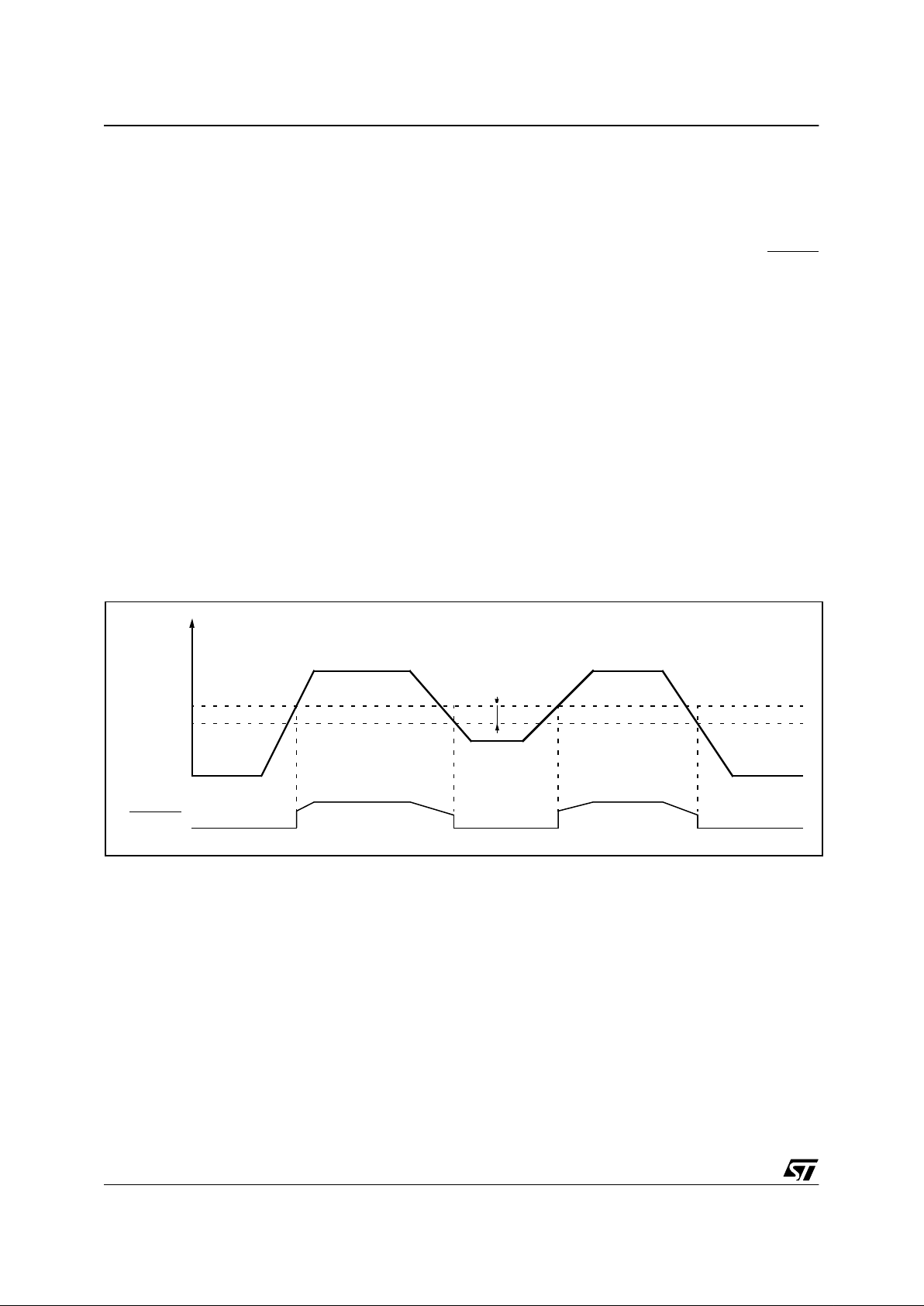
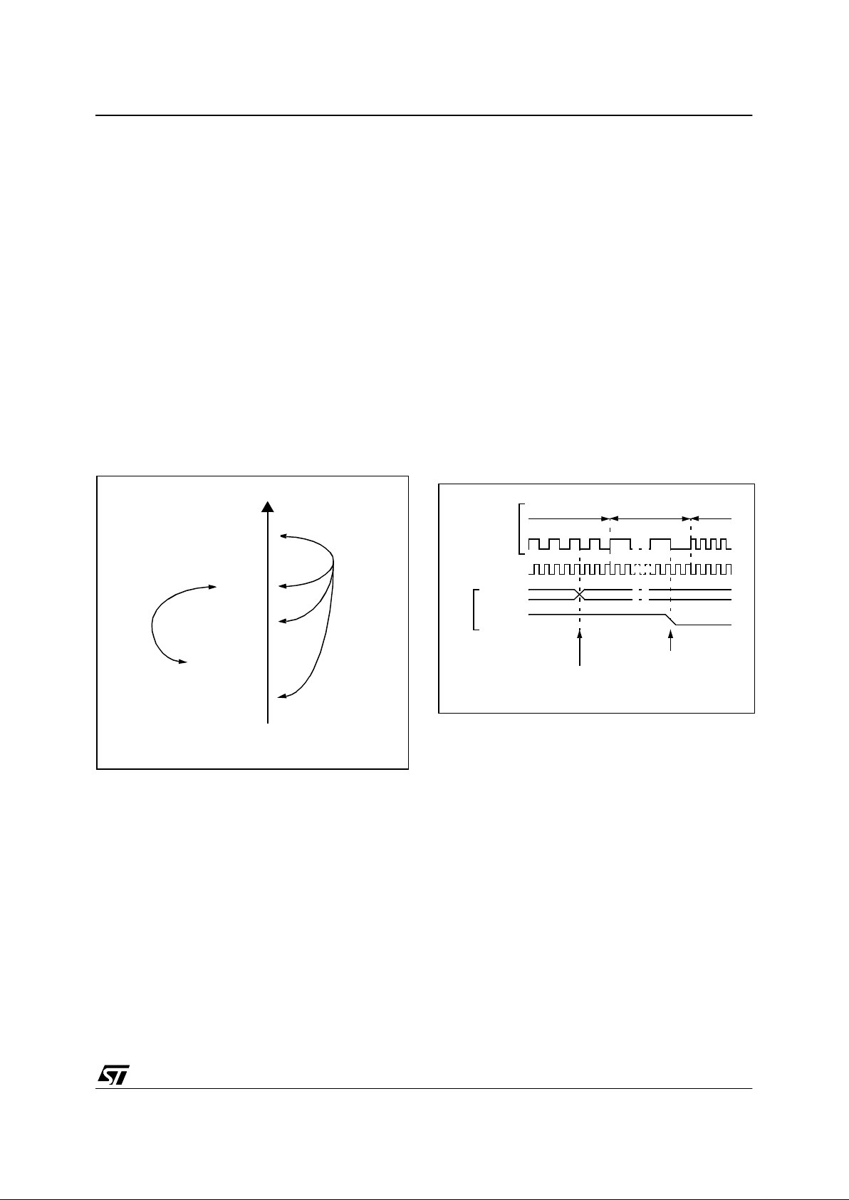
4.2 LOW VOLTAGE DETECTOR (LVD)
To allow the integration of power management
features in the application, the Low Voltage Detector function (LVD) generates a static reset when
the V
DD
supply voltage is below a V
IT-
reference
value. This means that it secures the power-up as
well as the power-down keeping the ST7 in reset.
The V
IT-
reference value for a voltage drop is lower
than the V
IT+
reference value for power-on in order
to avoid a parasitic reset when the MCU starts running and sinks current on the supply (hysteresis).
The LVD Reset circuitry generates a reset when
V
DD
is below:
–V
IT+
when VDD is rising
–V
IT-
when VDD is falling
The LVD func t ion is illustrated in the Figure .
Provided the minimum V
DD
value (guaranteed for
the oscillator frequency) is above V
IT-
, the MCU
can only be in two modes:
– under fu ll software control
– in static safe reset
In these conditions, secure operation is always ensured for the application without the need for external reset hardware.
During a Low Voltage Detector Reset, the RESET
pin is held low, thus p ermitting the MCU to reset
other devices.
Notes:
1. The LVD allows the device to be used without
any external RESET circuitry.
2. Three different reference levels are selectable
through the option byte according to th e application requirement.
LVD application note
Application software can detect a reset caus ed by
the LVD by reading the LVDRF bit in the CRSR
register.
This bit is set by hardware when a LVD reset is
generated and cleared by software (writing zero).
Figure 9. Low Voltage Detector vs Reset
V
DD
V
IT+
RESET
V
IT-
V
hyst
ST72C171
17/152
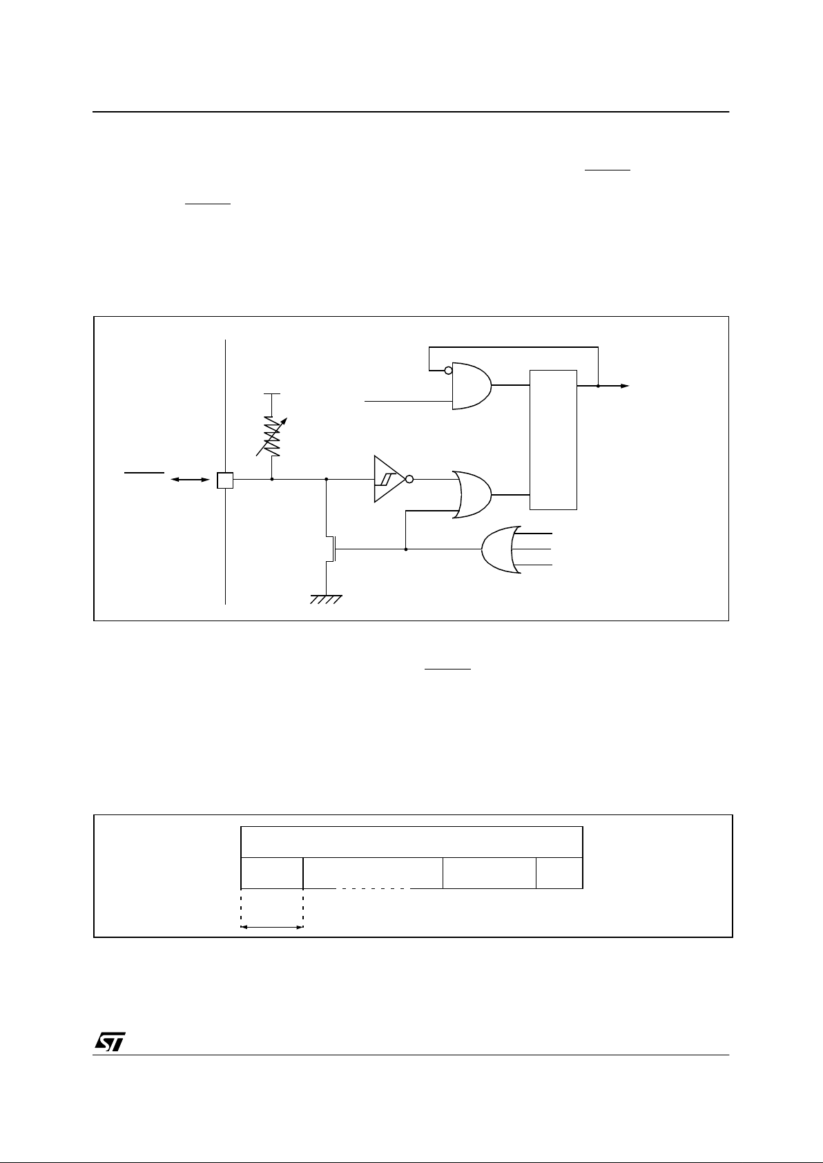
4.2.1 Reset Sequence Manager (RSM)
The RSM block of the CROSS Module includes
three RESET sources as shown in Figure 10:
■ EXTERNAL RESET SOURCE pulse
■ Internal LVD RESET (Low Voltage Detection)
■ Internal WATCHDOG RESET
These sources act on the RESET
PIN and it is always kept low during the READ OPTION RESET
phase.
The RESET service routine vector is fixed at the
FFFEh-FFFFh addresses in the ST7 memory
map.
Figure 10. Reset Block Diagram
The basic RESET s eque nc e cons i sts o f 4 p has es
as shown in Figure 11:
■ OPTION BYTE reading to configure the device
■ Delay depending on the RESET source
■ 4096 cpu clock cycle delay
■ RESET vector fetch
The duration of the OPTION BY TE reading phase
(t
ROB
) is defined in the Electrical Characteristics
section. This first phase is initiated by an external
RESET
pin pulse detection, a Watchdog RESET
detection, or when V
DD
rises up to V
LVDopt
.
The 4096 cpu clock cycle delay al lows the osci llator to stabilise and to ensure that recovery has taken place from the Reset state.
The RESET vector fetch phase duration is 2 clock
cycles.
Figure 11. RESET Sequence Phases
f
CPU
COUNTER
RESET
R
ON
V
DD
WATCHDOG RESET
LVD RESET
INTERNAL
RESET
READ OPTION RESET
RESET
READ
OPTION BYTE
INTERNAL RESET
4096 CLOCK CYCL ES
FETCH
VECTOR
DELAY
t
ROB
ST72C171
18/152
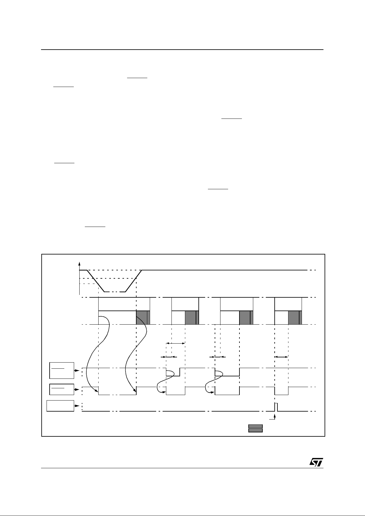
RESET SEQUENCE MANAGER (Cont’d)
4.2.2 Asynchronous External RES ET
pin
The RESET
pin is both an input and an open-drain
output with integrated R
ON
weak pull-up resistor.
This pull-up has no fixe d value but varies in accordance with the input voltage. It
can be pulled
low by external circuitry to reset the device. See
electrical characteristics section for more details.
A RESET signal originating from an external
source must have a duration of at least t
h(RSTL)in
in
order to be recognized. This detection is asynchronous and therefore the MCU can enter reset state
even in HALT mode.
The RESET
pin is an asynchronous signal which
plays a major role in EMS performance. In a noisy
environment, it is recommended to follow the
guidelines mentioned in the electr ical characteristics section.
Two RESET sequences can be associated with
this RESET source: short or long external reset
pulse (see Figure 12).
Starting from the external RESET pulse recognition, the device RESET
pin acts as an output that
is pulled low during at least t
w(RSTL)out
.
4.2.3 Inte r na l Lo w Volta ge Detection RESET
Two differen t RESET sequences caused by the internal LVD circuitry can be distinguished:
■ Power-On RESET
■ Voltage Drop RESET
The device RESET
pin acts as an output that is
pulled low when V
DD<VIT+
(rising edge) or
V
DD<VIT-
(falling edge) as shown in Figure 12.
The LVD filters spikes on V
DD
larger than t
g(VDD)
to
avoid parasitic resets.
4.2.4 Internal Watchdog RESET
The RESET sequence generated by a internal
Watchdog counter overflow is shown in Figure 12.
Starting from the Watchdog counter underflow, the
device RESET
pin acts as an output that is pulled
low during at least t
w(RSTL)out
.
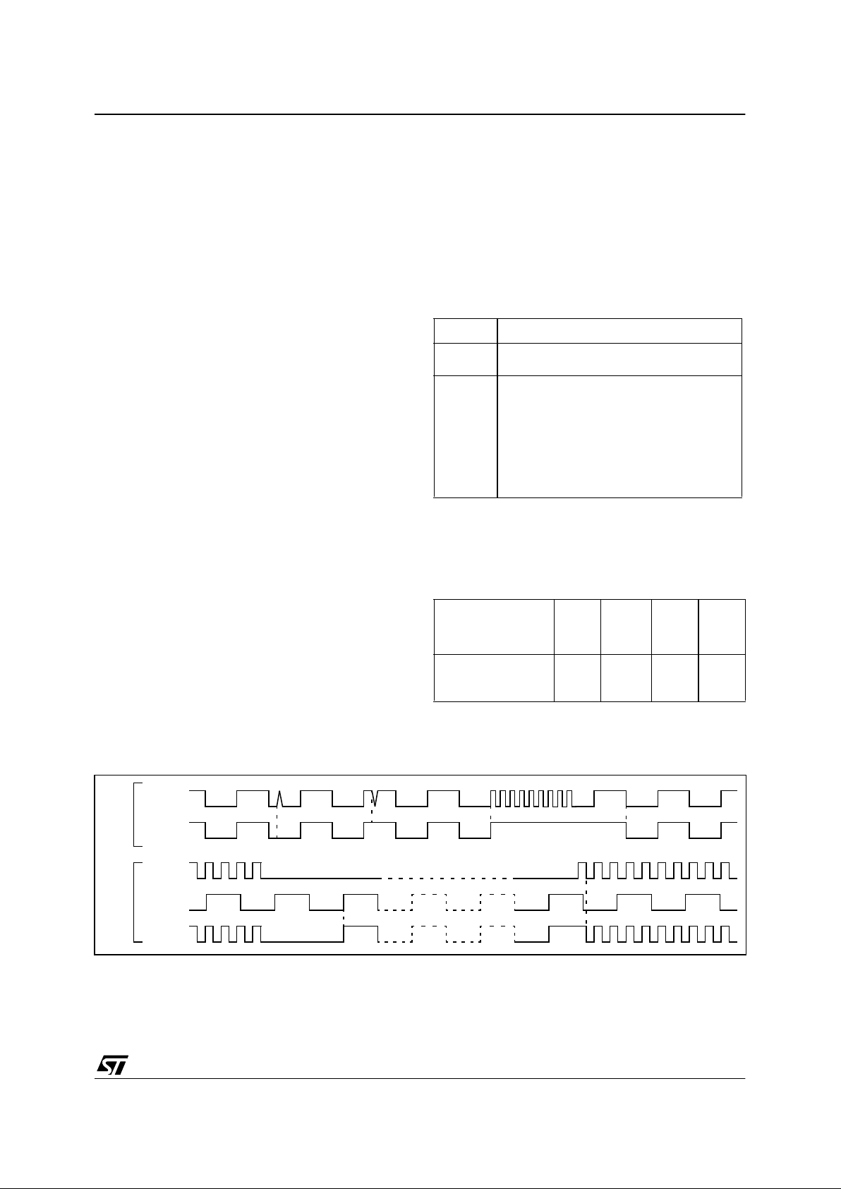
Figure 12. RESET Sequences
V
DD
RUN
RESET PIN
EXTERNAL
WATCHDOG
DELAY
V
IT+
V
IT-
t
h(RSTL)in
t
w(RSTL)out
RUN
DELAY
t
h(RSTL)in
DELAY
WATCHDOG UNDERFLOW
t
w(RSTL)out
RUN RUN
DELAY
RUN
RESET
RESET
SOURCE
SHORT EXT.
RESET
LVD
RESET
LONG EXT.
RESET
WATCHDOG
RESET
INTERNALRESET(4096 T
CPU
)
FETCH V ECTOR
ST72C171
19/152
4.2.4.1 Multi-Oscillator (MO)
The Mu lti-Oscillato r (MO) blo ck is the m ain clock
supplier of the ST7. To insure an optimum integration in the application, it is based on an external
clock source and six different selectable oscillators.
The main clock of t he ST 7 ca n be generated by 8
different sources comming from the MO block:
■ an External source
■ 4 Crystal or Ceramic resonator oscillators
■ 1 Extern al RC os cill ators
■ 1 Internal H igh Fre quency RC os c illator
Each oscillator is optimized for a given frequenc y
range in term of consumption and is selectable
through the Option Byte.
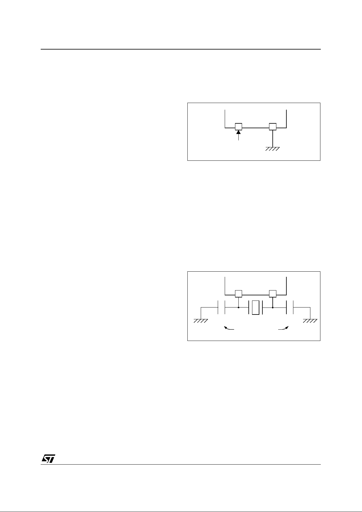
External Clock Source
The default Option Byte value selects the External
Clock in the MO block. In this mode, a clock signal
(square, sinus or triangle) with ~50% duty cycle
has to drive the OSCin pin while the OSCout pin is
tied to ground (see Figure 13).
Figure 13. MO Ex te rn a l Cl ock
Crystal/Ceramic Oscillators
This family of oscillators allows a high accuracy on
the main clock of the ST7. The selection within the
list of 4 oscillators has to b e done by Option Byte
according to the res onator frequency in order to
reduce the consum ption. In this mode of the MO
block, the resonator and the load capacitors have
to be connected as shown in Figure 14 a nd have
to be mounted as close as possible to the oscillator pins in order to minimize output distortion and
start-up stabilization time.
These oscillators, when selected via the Option
Byte, are not stopped during the RESET phas e to
avoid losing time in the oscillator starting phase.
Figure 14. MO Crystal/Ceramic Resonator
OSCin O SCout
EXTERNAL
ST7
SOURCE
OSCin OSCout
LOAD
CAPACIT ORS
ST7
C
L1
C
L0
ST72C171
20/152
MULTIOSCILLATO R (MO) (Cont’d)
External RC Oscillator
This oscillator allows a low cost solution on the
main clock of the ST7 using only an external resistor and an external capacitor (see Figure 15). T he
selection of the ex ternal RC oscillator has to be
done by Option Byte.
The frequency of the external RC oscillator is fixed
by the resistor and the capacitor values:
The previous formula shows that in this MO mode,
the accuracy of the clock is directly linked to the
accuracy of the discrete components.
Figure 15. MO External RC
Internal RC Oscillator
The Internal RC oscil lator mode is based on the
same principle as the External RC one including
the an on-chip resistor and capacitor. This mode is
the most cost effective one with the drawback of a
lower frequency accuracy. Its frequency is in the
range of several MHz.
In this mode, the two oscillator pins have to be tied
to ground as shown in Figure 16.
The selection of the internal RC oscillator has to
be done by Option Byte.
Figure 16. MO Internal RC
f
OSC
~
N
R
EX
. C
EX
OSCin OSCout
ST7
C
EX
R
EX
OSCin OSCout
ST7
ST72C171
21/152
4.3 CLOCK SECURITY SYSTEM (CSS)
The Clock Security System (CSS) protects the
ST7 against main clock problems. To allow the integration of the security features in the applications, it is based on a clock filter control and an Internal safe oscillator. The CSS can be enabled or
disabled by option byte.
4.3.1 Clock Filter Control
The clock filter is based on a clock frequency limitation function.
This filter function is able to detect and filter high
frequency spikes on the ST7 main clock.
If the oscillator is not working p roperly (e.g. working at a harmonic fr equency of the resonator), the
current active oscillator clock can be totally filtered, and then no clock signal is available for the
ST7 from this oscillator anymore. If the original
clock source recovers, the f iltering is s topped automatically and the oscillator supplies the ST7
clock.
4.3.2 Safe Oscillator Control
The safe oscillator of the CSS block is a low frequency back-up clock source (see Figur e 17).
If the clock signal disappears (due to a broken or
disconnected resonator...) during a safe o scillator
period, the safe oscillator delivers a low frequency
clock signal which allows the ST7 to perform some
rescue operations.
Automatically, the ST7 clock source switches back
from the saf e osc illa tor if the o rig inal clo ck s ourc e
reco ve rs .
Limitat io n det ect i on
The automatic safe oscillator selection is notif ied
by hardware setting the CSSD bit of the CRSR
register. An interrupt can be generat ed if the CSSIE bit has been previously set.
These two bits are described in the CRSR register
description.
4.3.3 Low Power Modes
4.3.4 Interrupts
The CSS interrupt event generates an interrupt if
the corresponding Enable Control Bit (CSSIE) is
set and the interrupt mask in the CC register is reset (RIM instruction).
Note 1: This interrupt allows to exit from active-halt
mode if this mode is available in the MCU.
Figure 17. Clock Filter Function and Safe Oscillator Function
Mode Description
WAIT
No effect on CSS. CSS interrupt cause the
device to exit from Wait mode.
HALT
The CRSR register is frozen. The CSS (including the safe oscillator) is disabled until
HALT mode is exited. The previous CSS
configuration resumes when the MCU is
woken up by an interrupt with “exit from
HALT mode” capability or from the counter
reset value when the MCU is woken up by a
RESET.
Interrupt Event
Event
Flag
Enable
Control
Bit
Exit
from
Wait
Exit
from
Halt
1)
CSS event detection
(safe oscillator activated as main clock)
CSSD CSSIE Yes No
f
OSC
/2
f
CPU
f
OSC
/2
f
CPU
f
SFOSC
SAFE OSCILLATOR
FUNCTION
CLOCK FILTER
FUNCTION
ST72C171
22/152
4.3.5 Main Clock Controller (MCC)
The MCC block supplies the clock for the ST7
CPU and its internal peripherals. It allows the power saving modes such as SLOW mode to be managed by the application.
All functions are managed by the Miscellaneous
Register 1 (MISCR1).
The MCC block consists of:
– a program mab le CPU clock prescaler
– a clock-out signal to supply external devices
The prescaler allows the selection of the main
clock frequency and is controlled with three bits of
the MISCR1: CP1, CP0 and SMS.
The clock-out capability is an Alternate Function of
an I/O port pin, providing the f
CPU
clock as an output for driving external devices. It is controlled by
the MCO bit in the MISCR1 register.
Figure 18. Main Clock Controller (MCC) Block Diagram
DIV 2, 4, 8, 16
DIV 2
SMS
CP1 CP0
CPU CLOCK
MISCR1
TO CPU AND
PERIPHERALS
f
OSC
MCO
PORT
FUNCTION
ALTERNATE
OSCOUT
OSCIN
MULTI-
OSCILLATOR
(MO)
CLOCK
FILTER
(CF)
MCO
f
CPU
ST72C171
23/152
4.4 CLOCK, RESET AND SUPPLY REGISTER DESCRIPTION
CLOCK RESET AND SUPPLY REGISTER
(CRSR)
Read/Write
Reset Value: 000x 000x (00h)
Bit 7:5 = Reserved.
Bit 4 = LV DRF
LVD Reset Flag
This bit indicates when set that the last Reset was
generated by the LVD block. It is set by hardware
(LVD reset) and cleared by software (writing zero)
or a Watchdog Reset. See WDGRF flag description for more details.
Bit 3 = Reserved.
Bit 2 = CSSIE
CSS Interrupt Enable
This bit allows to enable the interrupt whe n a distrurbance is detected by the Cloc k Security System (CSSD bit set). It is set and cleared by software.
0: Clock Filter interrupt disable
1: Clock Filter interrupt enable
Bit 1 = CSSD
CSS Safe Osc. Detection
This bit indicates that the safe oscillator of the CSS
block has been selected. It is set by hardware and
cleared by reading the CRSR register when the
original o s cilla t o r r ec o v er s.
0: Safe oscillator is not active
1: Safe oscillator has been activated
Bit 0 = WDGRF
WatchDog Reset Flag
This bit indicates when set that the last Reset was
generated by the Watchdog peripheral. It is set by
hardware (watchdog reset) and cleared by software (writing zero) or an LVD Reset.
Combined with the LVDRF flag information, the
flag description is given by the following table.
Table 3. Supply, Reset and Clock Register Map and Reset Values
70
---
LVD
RF
-
CSSIECSSDWDG
RF
RESET Sources LVDRF WDGRF
External RESET
pin 0 0
Watchdog 0 1
LVD 1 X
Address
(Hex.)
Register
Label
76543210
0020h
MISCR
Reset Value
PEI3
0
PEI2
0
MCO
0
PEI1
0
PEI0
0
CP1
0
CP0
0
SMS
0
0025h
CRSR
Reset Value
-
0
-
0
-
0
LVDRF
x
-
0
CSSIE0CSSD0WDGRF
x

ST72C171
24/152
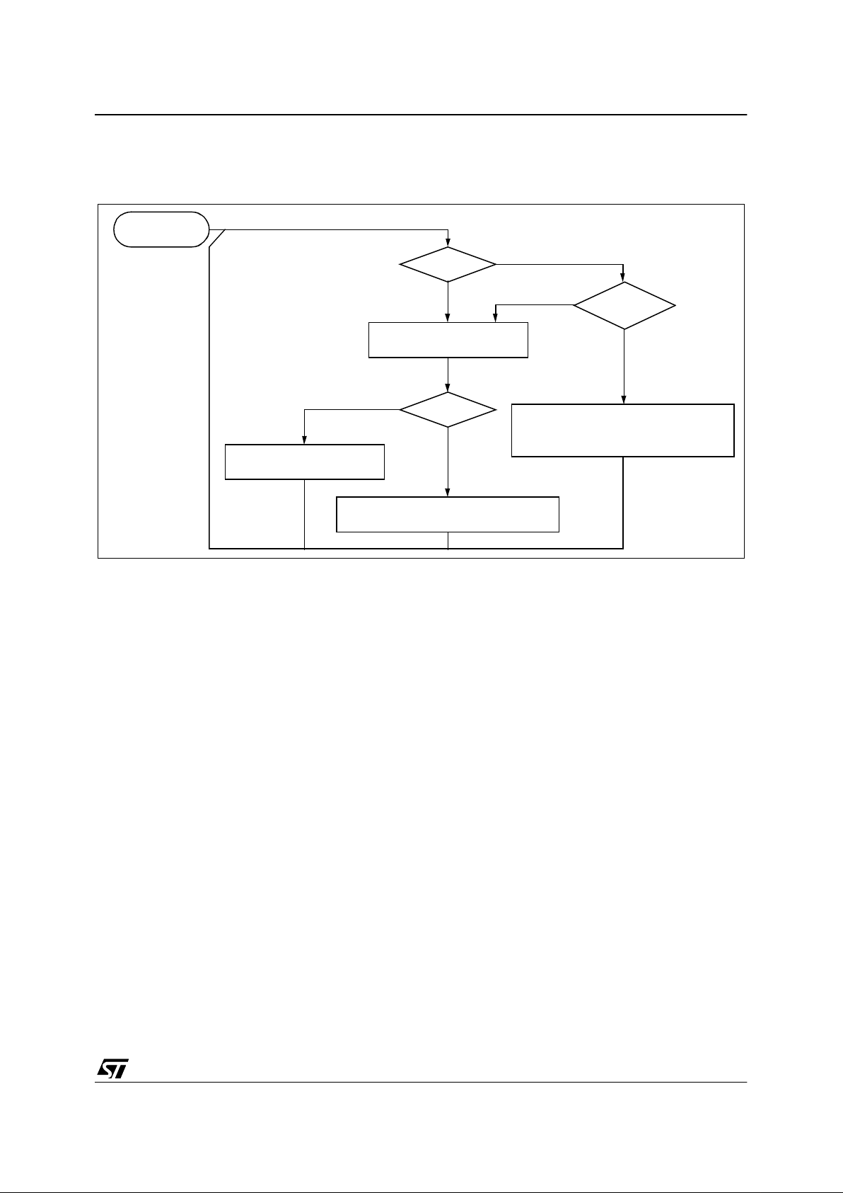
5 INTE RRUPTS
The ST7 core may be interrupted by one of two different methods: maskable hardware interrupts as
listed in the Interrupt Mapping Table and a nonmaskable software interrupt (TRAP). The Interrupt
processing flowchart is shown in F igure 19.
The maskable interrupts must be enabled clearing
the I bit in order to be serviced. However, disabled
interrupts may be latched and processed when
they are enabled (see external interrupts subsec tion) .
When an interrupt has to be serviced:
– No rmal processing is susp ended at the end of
the current instruction execution.
– The PC, X, A and CC registers are saved onto
the stack.
– The I bit of the CC register is set to prevent addi-
tional interrupts.
– The PC is then loaded with the interrupt vector of
the interrupt to service and the first instruction of
the interrupt service routine is fetched (refer to
the Interrupt Mapping Table for vector addresses).
The interrupt service routine should finish with the
IRET instruction which c auses the contents o f the
saved registers to be recovered from the stack.
Note: As a consequence of the IRET instruction,
the I bit will be cleared a nd the main pro gram will
resume.
Priority Management
By default, a servicing interrupt cannot be interrupted because the I bit is set by hardware entering in interrupt routine.
In the case when several inte rrupt s ar e simultaneously pending, an hardware priority defines which
one will be serviced first (see the Interrupt Mapping Table).
Interrupts and Low Power Mode
All interrupts allow the processor to leave the
WAIT low power mode. Only external and specifically mentioned interrupts allow the proc essor to
leave the HALT low power mode (refer to the “Exit
from HALT“ column in the I nterrupt Mapping Table).
5.1 NON MASKABLE SOFTWARE INTERRUPT
This interrupt is entered when the TRAP instruction is executed regardless of the state of the I bit.
It will be serviced according to the flowchart on
Figure 19.
5.2 EXTERNAL INTERRUPTS
External interrupt vectors can be loaded into the
PC register if the corresponding ext ernal interrupt
occurred and if the I bit is cleared. These interrupts
allow the processor to leave the Halt low power
mode.
The external interrupt polarity is selected through
the miscellaneous register or interrupt register (if
available).
An external interrupt triggered on edge will be
latched and the interrupt request automatically
cleared upon entering the interrupt service routine.
If several input pins, connected to the same interrupt vector, are configured as interrupts, their signals are logically ANDed before entering the edge/
level detection block.
Caution: The type of sensitivity defined in the Miscellaneous or Interrupt register (if available) applies to the ei source. In case of an ANDed source
(as described on the I/O ports section), a low level
on an I/O pin configured as input with interrupt,
masks the interrupt request even in case of risingedge sensitivity.
5.3 PERIPHERAL INTERRUPTS
Different peripheral interrupt flags in the status
register are able to cause an interrupt when they
are active if both:
– The I bit of the CC register is cleared.
– The corresponding enable bit is set in the control
register.
If any of these two conditions is false, the interrupt
is latched and thus remains pending.
Clearing an interrupt request is done by:
– Writing “0” to the corresponding bit in the status
register or
– Access to the status register while the f lag i s set
followed by a read or write of an associated register.
Note: the clearing sequence resets the internal
latch. A pending interrupt (i.e. waiting for being enabled) will therefore be lost if the clear sequence is
executed.
ST72C171
25/152
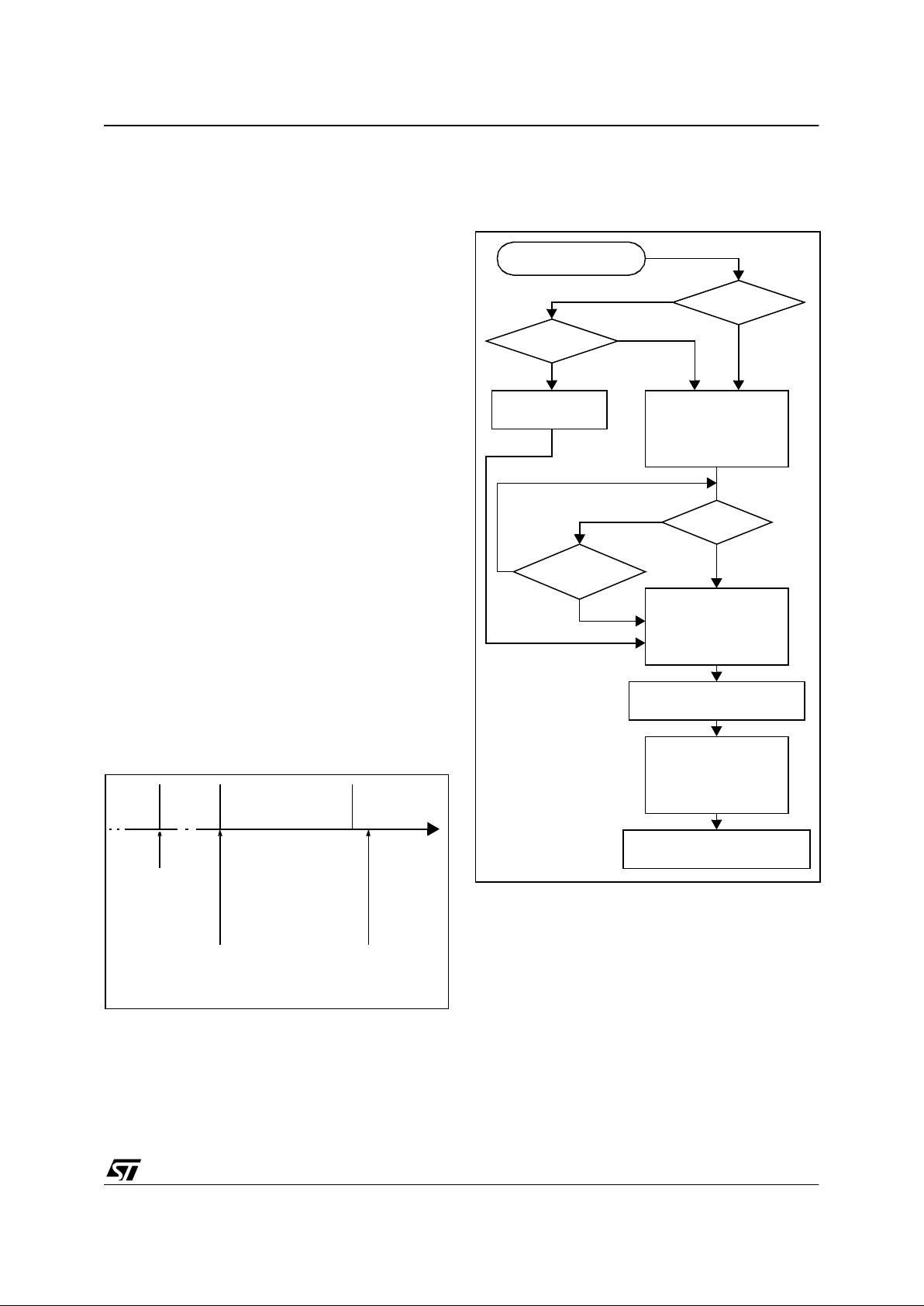
INTERRUPTS (Cont’d)
Figure 19. Inte rru pt P rocessing Flow chart
I BIT SET?
Y
N
IRET?
Y
N
FROM RESET
LOAD PC FROM INTERRUPT VECTOR
STACK PC, X, A, CC
SET I BIT
FETCH NEXT INSTRUCTION
EXECUTE INSTRUCTION
THIS CLEARS I BIT BY DEFAULT
RESTORE PC, X, A, CC FROM STACK
INTER RUPT
Y
N
PENDING?
ST72C171
26/152
INTERRUPTS (Cont’d)
Table 4. Int errupt Mappin g
Source
Block
Description
Register
Label
Flag
Exit from
HALT
Vector
Address
Priority
Order
RESET Reset N/A N/A yes FFFEh-FFFFh
TRAP Software N/A N/A no FFFCh-FFFDh
ei0 Ext. Interrupt ei0 N/A N/A yes FFFAh-FFFBh
ei1 Ext. Interrupt ei1 N/A N/A yes FFF8h-FFF9h
CSS Clock Filter Interrupt CRSR CSSD no FFF6h-FFF7h
SPI
Transfer Complete
SPISR
SPIF
no FFF4h-FFF5h
Mode Fault MODF
TIMER 16
Input Capture 1
TASR
ICF1_1
no FFF2h-FFF3h
Output Compare 1 OCF1_1
Input Capture 2 ICF2_1
Output Compare 2 OCF2_1
Timer Overflow TOF_1
ART/PWM
Input Capture 1 ARTICCSR ICF0
yes
FFF0h-FFF1h
Timer Overflow ARTCSR OVF FFEEh-FFEFh
OP-AMP
OA1 Interrupt
OIRR
OA1V
yes
FFECh-FFEDh
OA2 Interrupt OA2V FFEAh-FFEBh
NOT USED FFE6-FFE9
SCI SCI Peripheral Interrupts no FFE4-FFE5
NOT USED FFE0h-FFE3h
Highest
Priority
Priority
Lowest
ST72C171
27/152
6 POWER SAVIN G MO DES
6.1 INTRODUCTION
To give a large measure of flexibility to the application in terms of power consumption, three main
power saving modes are implemented in the ST7
(see Figure 20).
After a RESET the normal operating mode is selected by default (RUN mode). This mode drives
the device (CPU and embedded peripherals) by
means of a master clock which is based on the
main oscillator frequency divided by 2 (f
CPU
).
From Run mode, the different power saving
modes may be selected by setting the relevant
register bits or by calling the specific ST7 software
instruction whose action depends on the the oscillator status.
Figure 20. P ower Saving Mo de Transitions
6.2 SLOW MODE
This mode has two targets:
– To reduce power consumption by decreasing the
internal clock in the device,
– To adapt the internal clock frequency (f
CPU
) to
the available supply voltage.
SLOW mode is controlled by three bits in the
MISCR1 register: the SMS bit which enables or
disables Slow mode and two CPx bits which select
the internal slow frequency (f
CPU
).
In this mode, the oscillator frequency can be divided by 4, 8, 16 or 32 instead of 2 in norm al ope ra ting mode. The CPU and peripherals are clocked at
this lower frequency.
Note: SLOW-WAIT mode is activated when enterring the WAIT mode while the device is already in
SLOW mode.
Figure 21. SLOW Mode Clock Transitions
POWER CONSUMPTION
WAIT
SLOW
RUN
HALT
High
Low
SLOW WAIT
00 01
SMS
CP1:0
f
CPU
NEW SLOW
NORMALRUN MODE
MISCR1
FREQUENCY
REQUEST
REQUEST
f
OSC
/2
f
OSC
/4 f
OSC
/8 f
OSC
/2
ST72C171
28/152
POWER SAVING MODES (Cont’d)
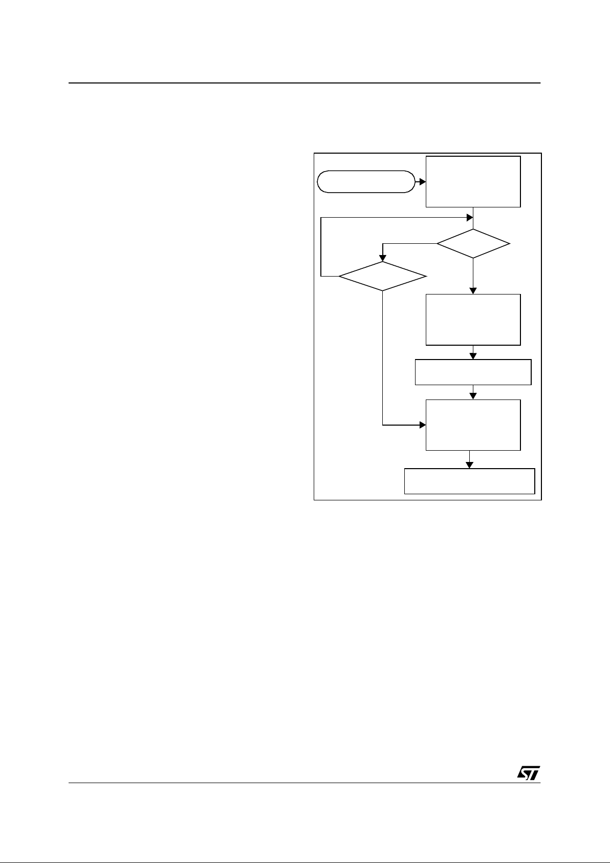
6.3 WAIT MODE
WAIT mode places the MCU in a low power consumption mode by stopping the CPU.
This pow er s av in g mode is s elected by ca llin g the
“WFI” ST7 software instruction.
All peripherals remain active. During WAIT mode,
the I bit of the CC register are forced to 0, to enable all interrupts. All other registers and memory
remain unchanged. The MCU remains in WAIT
mode until an interrupt or Reset occu rs, where upon the Program Counter branc hes to the starting
address of the interrupt or Reset service routine.
The MCU will r e main in W AIT mod e unt il a Rese t
or an Interrupt occurs, causing it to wake up.
Refer to Figure 22.
Figure 22. WAIT Mode Flow-chart
Note: Before servicing an interrupt, the CC regis-
ter is pushed on the stack. The I bit of the CC register is set during the interrupt routine and cleared
when the CC register is popped.
WFI INSTRUCTION
RESET
INTERRUPT
Y
N
N
Y
CPU
OSCILLATOR
PERIPHERALS
I BIT
ON
ON
0
OFF
FETCH RESET VECTOR
OR SERVICE INTERRUPT
CPU
OSCILLATOR
PERIPHERALS
I BIT
ON
OFF
1
ON
CPU
OSCILLATOR
PERIPHERALS
I BIT (s ee note)
ON
ON
1
ON
4096 CPU CLOCK CYCLE
DELAY
ST72C171
29/152
POWER SAVING MODES (Cont’d)
6.4 HALT MODE
The HALT mode is the lowest power consumption
mode of the MCU. It is entered by executing the
ST7 HALT instruction (see Figure 24).
The MCU can exit HALT m ode on reception of either an specific interrupt (see Table 4, “Interrupt
Mapping,” on page 26) or a RESET. When exiting
HALT mode by means of a RESET or an interrupt,
the oscillator is immediately turned on and the
4096 CPU cycle delay is used to stabilize the oscillator. After the start up delay, the CPU resumes
operation by servicing the i nterrupt or by fetching
the reset vector which woke it up (see Figure 23).
When entering HALT mode, the I bit in the CC register is forced to 0 to e nable interrupt s. Therefore,
if an interrupt is pending, the MCU wakes immediately.
In the HALT mode the m ain oscillator is t urned o ff
causing all internal processing to be stopped, including the operation of the on-chip peripherals.
All peripherals are not clocked except the ones
which get their clock supply from another clock
generator (such as an external or auxiliary oscillator).
The compatibility of Watchdog operation with
HALT mode is configured by t he “WD GHA LT” option bit of the option byte. The HALT instruction
when executed while the Watchdog system is enabled, can generate a Watchdog RESET (see
Section 11.1 OPTION BYTES for more details).
Figure 23. HALT Mode Timing Overview
Figure 24. HALT Mode Flow - chart
Notes:
1. WDGHALT is an option bit. See option byte sec-
tion for more details.
2. Peripheral clocked with an external clock source
can still be active.
3. Only some spec ific interrupt s can exit the MCU
from HALT mode (su ch as ex ternal i nterrupt). Refer to Table 4, “Interrupt Mapping,” on page 26 for
more details.
4. Before servicing an interrupt, the CC register is
pushed on the stack. The I bit of the CC register is
set during the interrupt routine and cleared when
the CC register is popped.
HALTRUN RUN
4096 CPU CYCLE
DELAY
RESET
OR
INTERRUPT
HALT
INSTRUCTION
FETCH
VECTOR
HALT INSTRUCTION
RESET
INTERRUPT
3)
Y
N
N
Y
CPU
OSCILLATOR
PERIPHERALS
2)
I BIT
OFF
OFF
0
OFF
FETCH RESET VECTOR
OR SERVICE INTERRUPT
CPU
OSCILLATOR
PERIPHERALS
I BIT
ON
OFF
1
ON
CPU
OSCILLATOR
PERIPHERALS
I BIT
4)
ON
ON
1
ON
4096 CPU CLOCK CYCLE
DELAY
WATCHDO G
ENABLE
DISABLE
WDGHALT
1)
0
WATCHDOG
RESET
1

ST72C171
30/152
7 ON-CHIP PERIPHERALS
7.1 I/O PORTS
7.1.1 Introd uct i on
The I/O ports offer different functional modes:
– transfer of data through digital inputs and outputs
and for specific pins:
– analog signal input (ADC)
– alternate signal input/output for the on-chip pe-
ripherals.
– external interrupt generation
An I/O port is composed of up to 8 pins. Each pin
can be programmed independently as digital input
(with or without interrupt generation) or digital output.
7.1.2 Functional Description
Each port is associated to 2 main registers:
– Data Register (DR)
– Data Direction Register (DDR)
and some of them to an optional register (see reg-
ister description):
– Option Register (OR)
Each I/O pin may be programmed using the corre-
sponding register bits in DDR and OR registers: bit
X corresponding to pin X of the port. The same correspondence is used for the DR register.
The following description takes into account the
OR register, for specific ports which do not provide
this register refer to the I/O Port Implementation
Section 7.1.2.5. The generic I/O block diagram is
shown on Figure 26.
7.1.2.1 Input Modes
The input configuration is sele cted by clearing the
corresponding DDR register bit.
In this case, reading the DR register returns the
digital value applied to the external I/O pin.
Different input modes can be selected by software
through the OR register.
Notes:
1. All the inputs are triggered by a Schmitt trigger.
2. When switching from input mode to output
mode, the DR register should be written first to
output the correct value as soon as the port is configured as an output.
Interrupt function
When an I/O is configured in Input with Interrupt,
an event on thi s I/O can generat e an external Interrupt request to the CPU. The interrupt sensitivity is given independently according to the description mentioned in the Miscellaneous register or in
the interrupt register (where available).
Each pin can independently generate an Interrupt
request.
Each external interrupt vector is linked t o a dedicated group of I/O port pins (see Interrupts section). If more than one input pin is selected simultaneously as interrupt source, this is logically
ORed. For this reason if one of the interrupt pins is
tied low, it masks the other ones.
7.1.2.2 Output Mode
The pin is configured in output mode by setting the
corresponding DDR register bit.
In this mode, writing “0” or “1” to the DR register
applies this digital value to the I/O pin through the
latch. Then reading the DR register returns the
previously stored value.
Note: In this mode, the interrupt function is disabled.
7.1.2.3 Digital Alternate Function
When an on-chip peripheral is configured to use a
pin, the alternate function is au tomatically selected. This alternate function takes priority over
standard I/O programming. When the signal is
coming from an on-chip peripheral, the I/O pin is
automatically configured in output mode (push-pull
or open drain according to the peripheral).
When the signal is goi ng to an on-chip peripheral,
the I/O pin ha s to be configured in i nput mode. In
this case, the pin’s state is a lso digitally readable
by addressing the DR register.
Notes:
1. Input pull-up configuration can cause an unex pected value at the input of the alternate peripheral input.
2. When the on-chip peripheral uses a pin as input
and output, this pin must be configured as an input
(DDR = 0).
Warning
: The alternate func tion m us t not be a cti-
vated as long as the pin is configured as input with
interrupt, in order to avoid generating spurious interrupts.
 Loading...