

SGS Thomson Microelectronics ST70235A Datasheet
ST70235A
ASCOTTM DMT TRANSCEIVER
PRELIMINARY DATA
■ DMT MODEM FOR CPE ADSL,
COMPATIBLE WITH THE FOLLOWING
STANDARDS:
- ANSI T1.413 ISSUE 2
- ITU-T G.992.1 (G.DMT)
- ITU-T G.992.2 (G.LITE)
■ SUPPORTS EITHER ATM (UTOPIA LEVEL
1 & 2) OR BITSTREAM INTERFACE
■ 16 BIT MULTIPLEXED MICROPROCESSOR
INTERFACE (LITTLE AND BIG ENDIAN
COMPATIBILITY)
■ ANALOG FRONT END MANAGEMENT
■ DUAL LATENCY PATHS: FAST AND
INTERLEAVED
■ ATM’S PHY LAYER: CELL PROCESSING
(CELL DELINEATION, CELL INSERTION,
HEC)
■ ADSL’ S OV ER HEAD MANAG EMEN T
■ REED SOLOMON ENCODE/DECODE
■ TRELLIS ENCODE/DECODE (VITERBI)
GENERAL DESCRIPTION
The ST70235A is the DMT modem and ATM
framer of the STMicroelectronics ASCOT™
chipset. When coupled with ST70134 analog
front-end and an external controller running
dedicated firmware, the product fulfills ANSI
T1.413 "Issue 2" DMT ADSL specification. The
chip supports UTOPIA level 1 and UTOPIA level 2
interface.
The ST70235A can be split up into two different
sections. The physical one performs the
DMT modulation, demodulation, Reed-Solomon
encoding, bit interleaving and 4D trellis coding.
The ATM section embodies framing f unctions for
the generic and ATM Tran smission Convergence
(TC) layers. The generic TC consists of data
scrambling and Ree d Solomon error corrections,
with and without interleaving.
The ST70235A is controlled and programmed
by an external controller (ADSL Transceiver Controller, ATC) that sets the programmable coefficients. The firmware controls the initialization
phase and carries out the consequent adapt ation
operations.
■ DMT MAPPING / DEMAPPING OVER 256
CARRIERS
■ FINE (2PPM) TIMING RECOVER USING
ROTOR AND ADAPTATIVE FREQUENCY
DOMAIN EQUALIZING
■ TIME DOMAIN EQUALIZATION
■ FRON T E ND DIGI TAL FILTERS
■ 0.25µm HCMOS7 TECHNOLOGY
■ 144 PIN TQFP
TQFP144 Full Plastic
(20 x 20 x 1.40 mm)
■ POWER CONSUMPTION: 0.4 WA T T
APPLICATIONS
Routers at SOHO, stand-alone modems, PC
modems.
This is advance information on a new product now in development or undergoing evaluation. Details are subject to change without notic e.
ORDER CODE: ST70235A
1/28October 2001
ST70235A
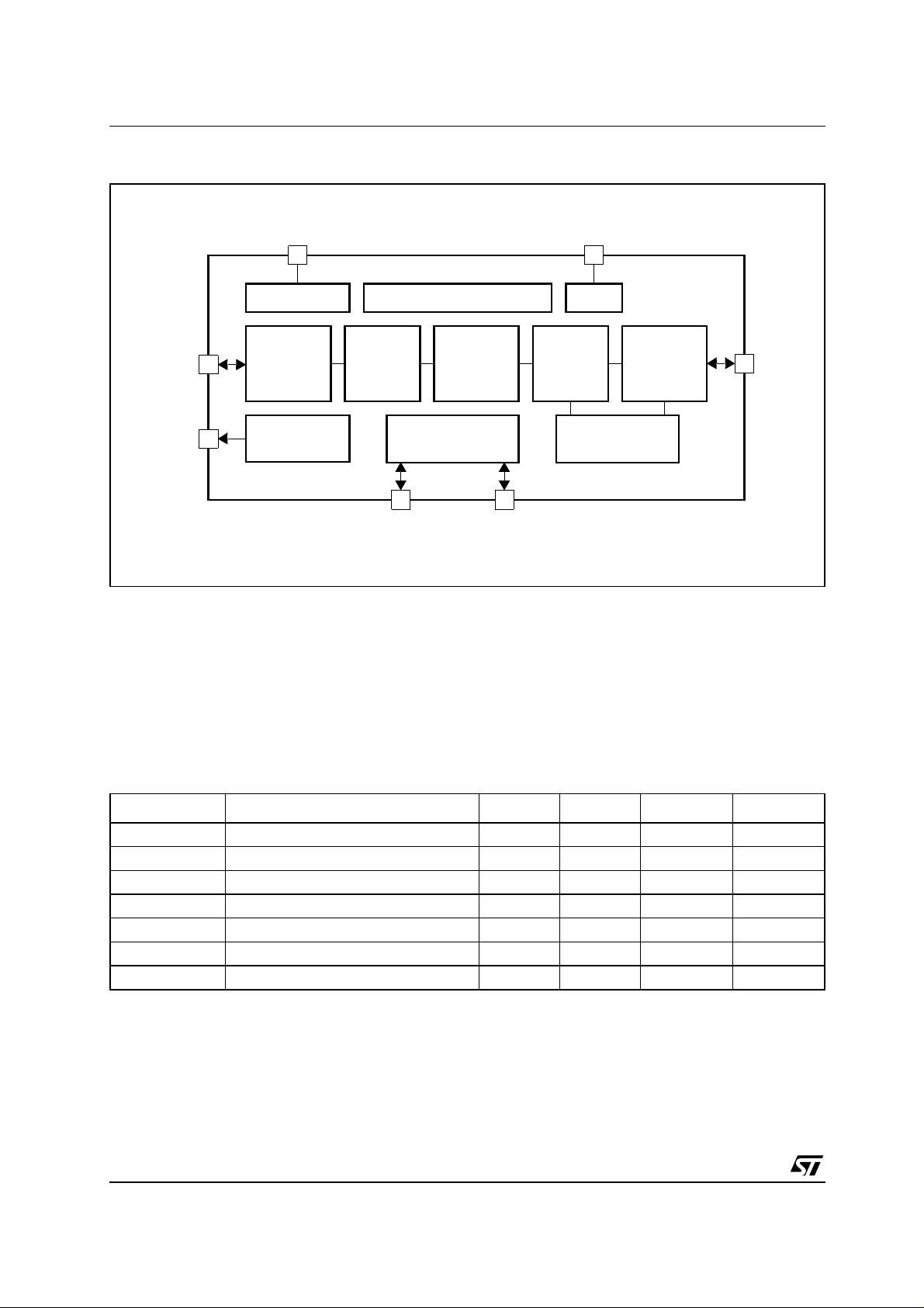
Figure 1 : Block Diagram
TEST SIGNALS CLOCK
TEST MODULE DATA SYMBOL TIMING UNIT VCXO
AFE
INTERFACE
AFE
CONTROL
DSP
FRONT-END
AFE CONTROL
INTERFACE
FFT/IFFT
ROTOR
CONTROLLER
CONTROLLER
BUS
TRELLIS
CODING
MAPPER/
DEMAPPER
INTERFACE
GENERAL
PURPOSE I/Os
GENERIC
TC
REED/
SOLOMON
SPECIFIC TC
ATM
INTERFACE
MODULE
UTOPIA
Transient Ener gy Capabilities
ESD (Electronic Discharged) tests have been performed for the Human Body Model (HBM) and for the
Charged Device Model (CDM).
The pins of the device are t o be ab le to withstand minimum 2000V f or the HBM an d mini mum 250V for
CDM.
Latch-up
The maximum sink or source current from any pin is limited to 200mA to prevent latch-up.
ABSOLUTE MAXIMUM RATINGS
Symbol Parameter Min. Typ. Max. Unit
V
3.3 Supply Voltage 3.0 3.3 3.6 V
DD
1.8 Supply Voltage 1.62 1.8 1.98 V
V
DD
P
tot
T
amb
J/A Thermal Resistivity 38 °C/W
R
th
I
3.3
I
1.8
Total Powe r Dissipatio n 300 400 m W
Ambient Temperature 1m/s airflow 0 70 °C
Current Consumption 14 mA
Current Consumption 135 mA
2/28
Figure 2 : Pin Connection
AFTXD_1
AFTXD_0
IDDq
AD_0
AD_1
AD_2
VDD 3.3
AD_3
AD_4
AD_5
AD_6
VDD 3.3
AD_7
AD_8
AD_9
AD_10
AD_11
VDD 1.8
AD_12
PCLK
VDD 3.3
AD_13
AD_14
AD_15
VDD 3.3
WR_RDB
RDYB
OBC_TYPE
RESETB
CSB
INTB
VDD 3.3
AFTXD_3
AFTXD_2
VSS
144 143 142 141
VSS
1
2
3
4
5
6
7
8
VSS
9
10
11
12
13
14
VSS
15
16
17
18
19
VSS
20
21
22
23
24
25
VSS
26
BE1
27
ALE
28
29
30
31
32
33
34
35
VSS
36
37 38 39 40
ST70235A
AFRXD_1
AFRXD_0
VDD 3.3
PDOWN
GP_OUT
TESTSE
TRSTB
VSS
TCK
VDD 3.3
TMS
TDO
TDI
RESERVED
RESERVED
VDD 1.8
RESERVED
DISABLE_COMP
VSS
COMP_ROUT
COMP_VDD_1.8
VDD 3.3
CTRLDATA
MCLK
CLWD
VSS
AFRXD_3
AFRXD_2
134 133 132 131 130 129 128 127 126 125140 139 138 137 136 135
118 117 116 115 114 113 112 111 110 109124 123 122 121 120 119
ST70235A
47 48 49 50 51 52 5 3 54 55 5641 42 43 44 45 46
63 64 65 66 67 68 69 70 71 7257 58 59 60 61 62
VSS
VDD 1.8
108
RESERVED
107
RESERVED
106
RESERVED
105
RESERVED
104
RESERVED
103
VSS
102
RESERVED
101
RESERVED
100
RESERVED
99
RESERVED
98
RESERVED
97
RESERVED
96
VDD 3.3
95
RESERVED
94
RESERVED
93
RESERVED
92
VSS
91
RESERVED
90
U_TX_ADDR_0
89
U_TX_ADDR_1
88
U_TX_ADDR_2
87
VDD 1.8
86
U_TX_ADDR_3
85
U_TX_ADDR_4
84
U_TX_DATA_0
83
U_TX_DATA_1
82
VDD 1.8
81
U_TX_DATA_2
80
U_TX_DATA_3
79
U_TX_DATA_4
78
U_TX_DATA_5
77
VDD 3.3
76
U_TX_DATA_6
75
U_TX_DATA_7
74
VSS
73
U_RX_ADDR_2
U_RX_ADDR_3
VSS
GP_IN0
U_RX_ADDR_4
VSS
GP_IN1
VDD 3.3
U_TX_REFB
U_RX_REFB
VDD 1.8
U_RXCLK
U_RXSOC
U_RXCLAV
U_RXENBB
VSS
U_TXCLK
VDD 3.3
U_TXSOC
U_TXENBB
U_TX_CLAV
VSS
VDD 1.8
U_RXDATA_4
U_RXDATA_5
U_RXDATA_6
U_RXDATA_7
VDD 3.3
U_RX_ADDR_0
U_RX_ADDR_1
U_RXDATA_0
U_RXDATA_1
VSS
U_RXDATA_2
U_RXDATA_3
VDD 3.3
3/28
ST70235A
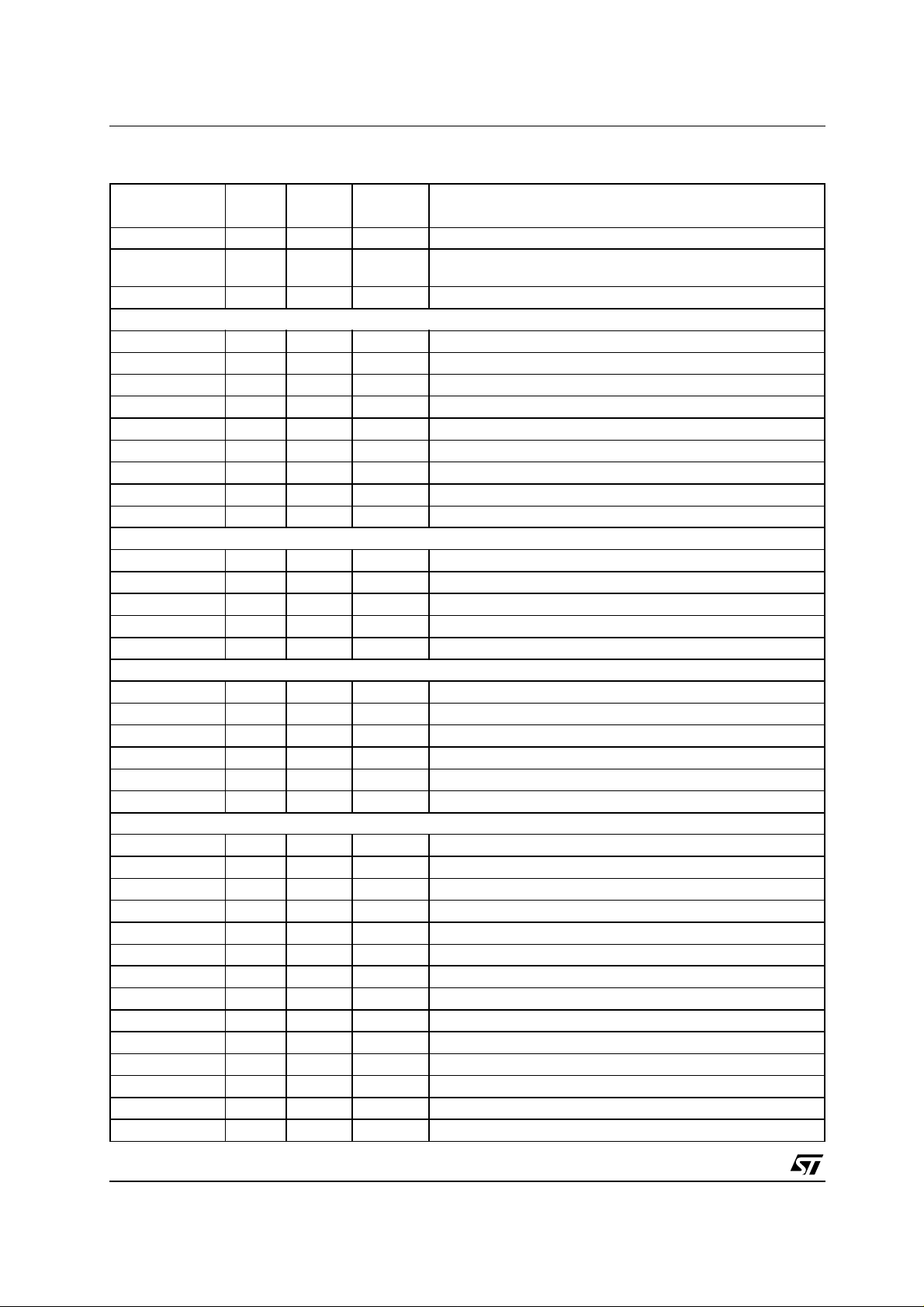
PIN FUNCTIONS
Pin Name Type
1 VSS 0V Ground
2 AD_0 B BD8STARP B Data 0
3 AD_1 B BD8STARP B Data 1
4 AD_2 B BD8STARP B Address / Data 2
5 VDD 3.3 (VSS + 3.3V) Power Supply
6 AD_3 B BD8STARP B Address / Data 3
7 AD_4 B BD8STARP B Address / Data 4
8 VSS 0V Ground
9 AD_5 B BD8STARP B Address / Data 5
10 AD_6 B BD8STARP B Address / Data 6
11 VDD 3.3 (VSS + 3.3V) Power Supply
12 AD_7 B BD8STARP B Address / Data 7
13 AD_8 B BD8STARP B Address / Data 8
14 AD_9 B BD8STARP B Address / Data 9
15 VSS 0V Ground
16 AD_10 B BD8STARP B Address / Data 10
17 AD_11 B BD8STARP B Address / Data 11
18 VDD 1.8 (VSS + 1.8V) Power Supply
19 AD_12 B BD8STARP B Address / Data 12
20 VSS 0V Ground
21 PCLK I TLCHT I Processor clock
22 VDD 3.3 (VSS + 3.3V) Power Supply
23 AD_13 B BD8STARP B Address / Data 13
24 AD_14 B BD8STARP B Address / Data 14
25 AD_15 B BD8STARP B Address / Data 15
26 VSS 0V Ground
27 BE1 I TLCHT I Address 1
28 ALE I TLCHT C Address Latch
29 VDD 3.3 (VSS + 3.3V) Power Supply
30 CSB I TLCHT I Chip Select
31 WR_RDB I TLCHT I Specifies the direction of the access cycle
32 RDYB OZ BD4STARP O Controls the ATC bus cycle termination
33 OBC_TYPE I-PD TLCHTDQ I ATC Mode Selection (0 = i960; 1 = generic)
34 INTB O BD4STARP O Requests ATC interrupt service
35 RESETB I TLCHT I Hard reset
36 VSS 0V Ground
37 VDD 3.3 (VSS + 3.3V) Power Supply
38 U_RxData_0 OZ BD8STARP B Utopia RX Data 0
39 U_RxData_1 OZ BD8STARP B Utopia RX Data 1
40 VSS 0V Ground
PAD Type
HCMOS7
BS Function
4/28
PIN FUNCTIONS (continued)
ST70235A
Pin Name Type
41 U_RxData_2 OZ BD8STARP B Utopia RX Data 2
42 U_RxData_3 OZ BD8STARP B Utopia RX Data 3
43 VDD 1.8 (VSS + 1.8V) Power Supply
44 U_RxData_4 OZ BD8STARP B Utopia RX Data 4
45 U_RxData_5 OZ BD8STARP B Utopia RX Data 5
46 VSS 0V Ground
47 U_RxData_6 OZ BD8STARP B Utopia RX Data 6
48 U_RxData_7 OZ BD8STARP B Utopia RX Data 7
49 VDD 3.3 (VSS + 3.3V) Power Supply
50 U_RxADDR_0 I TLCHT I Utopia RX Address 0
51 U_RxADDR_1 I TLCHT I Utopia RX Address 1
52 U_RxADDR_2 I TLCHT I Utopia RX Address 2
53 U_RxADDR_3 I TLCHT I Utopia RX Address 3
54 VSS 0V Ground
55 U_RxADDR_4 I TLCHT I Utopia RX Address 4
56 GP_IN_0 I-PD TLCHTDQ I General purpose input 0
57 VDD 3.3 (VSS + 3.3V) Power Supply
58 GP_IN_1 I-PD TLCHTDQ I General purpose input 1
59 VSS 0V Ground
60 U_RxRefB O BD4STARP O 8kHz clock to ATM device
61 U_TxRefB I TLCHT I 8kHz clock from ATM device
62 VDD 1.8 (VSS + 1.8V) Power Supply
63 U_Rx_CLK I T LCHT Utopia RX Clock
64 U_Rx_SOC OZ BD8STARP Utopia RX Start of Cell
65 U_RxCLAV OZ BD8STARP Utopia RX Cell Available
66 U_RxENBB I T LCHT Utopia RX Enable
67 VSS 0V Ground
68 U_Tx_CLK I T LCHT Utopia TX Clock
69 U_Tx_SOC I TLCHT Utopia TX Start of Cell
70 U_TxCLAV OZ BD8SCR Utopia TX Cell Available
71 U_TxENBB I T LCHT Utopia TX Enable
72 VDD 3.3 (VSS + 3.3V) Power Supply
73 VSS 0V Ground
74 U_TxData_7 I TLCHT I Utopia TX Data 7
75 U_TxData_6 I TLCHT I Utopia TX Data 6
76 VDD 3.3 (VSS + 3.3V) Power Supply
77 U_TxData_5 I TLCHT I Utopia TX Data 5
78 U_TxData_4 I TLCHT I Utopia TX Data 4
79 U_TxData_3 I TLCHT I Utopia TX Data 3
80 U_TxData_2 I TLCHT I Utopia TX Data 2
PAD Type
HCMOS7
BS Function
5/28
ST70235A
PIN FUNCTIONS (continued)
Pin Name Type
81 VDD 1.8 (VSS + 1.8V) Power Supply
82 U_TxData_1 I TLCHT I Utopia TX Data 1
83 U_TxData_0 I TLCHT I Utopia TX Data 0
84 U_TxADDR_4 I TLCHT I Utopia TX Address 4
85 U_TxADDR_3 I TLCHT I Utopia TX Address 3
86 VDD 1.8 (VSS + 1.8V) Power Supply
87 U_TxADDR_2 I TLCHT I Utopia TX Address 2
88 U_TxADDR_1 I TLCHT I Utopia TX Address 1
89 U_TxADDR_0 I TLCHT I Utopia TX Address 0
90 RESERVED BD4STARP Reserved 0
91 VSS 0V Ground
92 RESERVED BD4STARP Reserved 1
93 RESERVED BD4STARP Reserved 2
94 RESERVED BD4STARP Reserved 3
95 VDD 3.3 (VSS + 3.3V) Power Supply
96 RESERVED BD4STARP Reserved 4
97 RESERVED BD4STARP Reserved 5
98 RESERVED BD4STARP Reserved 6
99 RESERVED BD4STARP Reserved 7
100 RESERVED BD4STARP Reserved 8
101 RESERVED BD4STARP Reserved 9
102 VSS 0V Ground
103 RESERVED TLCHTDQ Reserved 10
104 RESERVED TLCHTDQ Reserved 11
105 RESERVED TLCHTDQ Reserved 12
106 RESERVED TLCHTDQ Reserved 13
107 RESERVED BD4STARP Reserved 14
108 VDD 1.8 (VSS + 1.8V) Power Supply
109 VSS 0V Ground
110 RESERVED BD4STARP Reserved 15
111 RESERVED BD4STARP Reserved 16
112 TDI I-PU TLCHTUQ JTAG I/P
113 TDO OZ BD4STARP JTAG O/P
114 TMS I-PU TLCHTUQ JTAG Made Select
115 VDD 3.3 (VSS + 3.3V) Power Supply
116 TCK I-PD TLCHTDQ JTAG Clock
117 VSS 0V Ground
118 TRSTB I-PD TLCHTDQ JTAG Reset
119 TESTSE I TLCHTDQ none Enables scan test mode
120 GP_OUT O BD8STARP O General purpose output
PAD Type
HCMOS7
BS Function
6/28
PIN FUNCTIONS (continued)
ST70235A
Pin Name Type
PAD Type
HCMOS7
BS Function
121 PDOWN O BD4STARP O Power down analog front end (Reset)
122 VDD 3.3 (VSS + 3.3V) Power Supply
123 AFRXD_0 I TLCHT I Receive data nibble
124 AFRXD_1 I TLCHT I Receive data nibble
125 AFRXD_2 I TLCHT I Receive data nibble
126 AFRXD_3 I TLCHT I Receive data nibble
127 VSS 0V Ground
128 CLWD I TLCHT I Start of word indication
129 MCLK I TLCHT C Master clock
130 CTRLDATA O BD4STARP O Serial data Transmit channel
131 VDD 3.3 (VSS + 3.3V) Power Supply
132 COMP_VDD_1.8 COMP_1V60 Compensation Cell VDD 1.8V (see note 1)
133 COMP_ROUT O COMP_1V60 none Compensation Cell Resistor (see note 1)
134 VSS COMP_1V60 0V Ground
135 DISABLE_COMP I TLCHTDQ Disable Compensation Cell (see note 1)
136 RESERVED Reserved
137 VDD 1.8 (VSS + 1.8V) Power Supply
138 IDDq I TLCHT none Test pin, active high
139 AFTXD_0 O BD8STARP O Transmit data nibble
140 AFTXD_1 O BD8STARP O Transmit data nibble
141 VSS 0V Ground
142 AFTXD_2 O BD8STARP O Transmit data nibble
143 AFTXD_3 O BD8STARP O Transmit data nibble
144 VDD 3.3 (VSS + 3.3V) Power Supply
Note: Compen sation cell - T he COMP_OUT pi n m ust be conne ct ed at GND by a 10 0KΩ resistor on board.
Specifications of t he resistor have to meet the followi ng requirements:
± 5% allowed on the value, ±1% is preferred.
Advice is given to place the resistor so that there will be the shortest path between it and the pin.
Using the DISABLE_COMP sig n al is possible to disable t he sle w ra te co nt ro l o f IO s, in this mode the IOs are howe ve r stil l functional,
but dynam i c performances are affec ted.
An inte rnal pull -down on DISABLE_COMP pin en abl es the slew rat e contro l of IOs, an external pu ll-up resistor (c onnected at 3.3 V)
must be inserted in order to disabl e the slew rate contro l .
Table 1 : I/O Driver Function
Driver Function
BD4STARP TTL Three Volt capable Schmitt Trigger Bidirectional Pad Buffer, 4mA, with T est pins, with Active Slew
Rate Control
BD8STARP TTL Three Volt capable Schmitt Trigger Bidirectional Pad Buffer, 8mA, with T est pins, with Active Slew
Rate Control
TLCHTDQ TTL Three Volt capable Input Buffer with Active Pull-Down and Test pin
TLCHTUQ TTL Three Volt capable Input Buffer with Active Pull-Up and Test pin
TLCHT TLL Three Volt capable Input Pad Buffer
7/28
ST70235A
PIN SUMMARY
Mnemonic Type BS Type
Power Supply
VDD 3.3
VDD 1.8
VSS 0V Ground
ATC INTERFACE
ALE I C 1 Used to latch the address of the internal register to be accessed
PCLK I I 1 Processor clock
CSB I I 1 Chip selected to respond to bus cycle
BE1 I I 1 Address 1 (not multiplexed)
WR_RDB I I 1 Specifies the direction of the access cycle
RDYB OZ O 1 Controls the ATC bus cycle termination
INTB O O 1 Requests ATC interrupt service
AD IO B 16 Multiplexed Addre ss/D ata bus
OBC_TYPE I-PD I 1 Select between i960 (0) or generic (1) controller interface
TEST ACCESS PART INTERFACE
TDI I- PU 1 Refer to section
TDO O Z 1
TCK I-PD 1
TMS I- PU 1
TRSTB I-PD 1
ANALOG FRONT END INTERFACE
AFRXD I I 4 Receive data nibble
AFTXD O O 4 Transmit data nibble
CLWD I I 1 Start of word indication
PDOWN O O 1 Power down analog front end
CTRLDATA O O 1 Serial data transm it channel
MCLK I C 1 Master cloc
ATM UTOPIA INTERFACE
U_RxData OZ B 8 Receive interface Data
U_TxData I I 8 Transmit interface Data
U_RxADDR I I 5 Receive interface Address
U_TxADDR I I 5 Transmit interface Address
U_RxCLAV OZ O 1 Receive interface Cell Available
U_TxCLAV OZ O 1 Transmit interface Cell Available
U_RxENBB I-TTL I 1 Receive interface Enable
U_TxENBB I-TTL I 1 Transmit interface Enable
U_RxSOC OZ O 1 Receive interface Start of Cell
U_TxSOC I-TTL I 1 Transmit interface Start of Cell
U_RxCLK I-TTL C 1 Receive interface Utopia Clock
U_TxCLK I-TTL C 1 Transmit interface Utopia Clock
U_RxRefB O O 1 8kHz reference clock to ATM device
U_TxRefB I-TTL I 1 8kHz reference clock from ATM device
Number
of Signals
Function
(VSS + 3.3V) Power supply
(VSS + 1.8V) Power supply
8/28
PIN SUMMARY (continued)
ST70235A
Mnemonic Type BS Type
MISCELLANEOUS
GP_IN I-PD I 2 General purpose input
GP_OUT O O 1 General purpose output
RESETB I I I Hard reset
TESTSE I none none Enable scan test mode
IDDq I none none Test pin, active high
COMP_ROUT O none 1 Compensation cell resistor
DISABLE_COMP
I-PD I 1 Disable compensation cell
I = Input, CMOS levels
I-PU = Input with pull-up resistance, TTL
levels
I-PD = Input with pull-down resistance, TTL
levels
I-TTL = Input TTL levels
O = Push-pull output
OZ = Push-pull output with high-impedance
state
IO = Input / Tristate Push-pull output
BS cell = Boundary -S can cell
I = In put c e ll
O = Output cell
B = Bidirectional cell
C=Clock
Number
of Signals
is to reduce the effect of Inter-Symbol
Interferences (ISI) by shortening the channel
impulse resp onse.
Both the Decimator and TEQ can be bypassed. In
the transmit direction, the DSP Front-End
includes: sidelobe filtering, clipping, delay
equalization and interpolation. The sidelobe
filtering and delay equalization are implemented
by IIR Filters, reducing the effect of echo in FDM
systems.
Clipping is a statistical process limiting the
amplitude of the output signal, optimizing the
dynamic range of the AFE. The interpolator
receives data at 2.2M Hz and generates samples
at a rate of 8.8MHz.
Main Block Description
The following drawings desc ribe the sequence of
functions performed by the chip.
DSP Fro nt- E nd
The DSP Front-End contains 4 parts in the
receive direction: the Input Selector, the Analog
Front-End Interface, the Decima tor and the Time
Equalizer.
The input selector is used internally to enable test
loopbacks inside the chip. The Analog Front-End
lnterface transfers 16-bit words, multiplexed on 4
input/output signals. Word transfer is carried out in
4 clock cycles.
The Decimator receives 16-bit samples at 8.8MHz
(as sent by the Analo g Front-End chip: S T70134)
and reduces this rate to 2.2MHz.
The Time Equalizer (TEQ) modul e is a FIR filter
with programmable coefficients. Its main purpose
DMT Modem
This module is a programmable DSP unit. Its
instruction set enables the basic functions of the
DMT algorithm like FFT, IFFT, Scaling, Rotor and
Frequency Equalization (FEQ) in c omplian ce with
ANSI T1.413 specifications.
In the RX path, the 512-po int FFT transforms the
time-domain DMT symbol into a frequency
domain representation which can be further
decoded by the subsequent demappin g stages.
In other words, the Fast Fourier Transform
process is used to transform from time domain to
frequency domain (receive path). 1024 time
samples are processed. After the first stage time
domain equalization and FFT block an ICI
(InterCarrier Interference) free informat ion stream
turns out.
Function
9/28
 Loading...