

SGS Thomson Microelectronics ST662ACN, ST662ACD, ST662ABN, ST662ABD Datasheet
ST662A
DC-DC CONVERTER FROM 5V TO 12V, 0.03A
FOR FLASH MEMORY PROGRAMMING SUPPLY
June 1997
■ OUTPUT VOLTAGE:12V± 5%
■ SUPPLYVOLTAGERANGE: 4.5V TO 5.5V
■ GUARANTEED OUTPUT CURRENT UPTO
30mA
■ VERYLOWQUIESCENTCURRENT: 100µA
■ LOGICCONTROLLEDELECTRONIC
SHUTDOWN: 1µA
■ JUSTCAPACITORSNEEDED(NO
INDUCTOR)
DESCRIPTION
The ST662A is a regulated charge pump DC-DC
converter.It provides12V ± 5% output voltage to
programbyte-wide flash memory, and can supply
30mA output current from inputas low as4.75V
A logic controlled shut down pin that interfaces
directly with microprocessor reduces the sypply
currentto only1µA
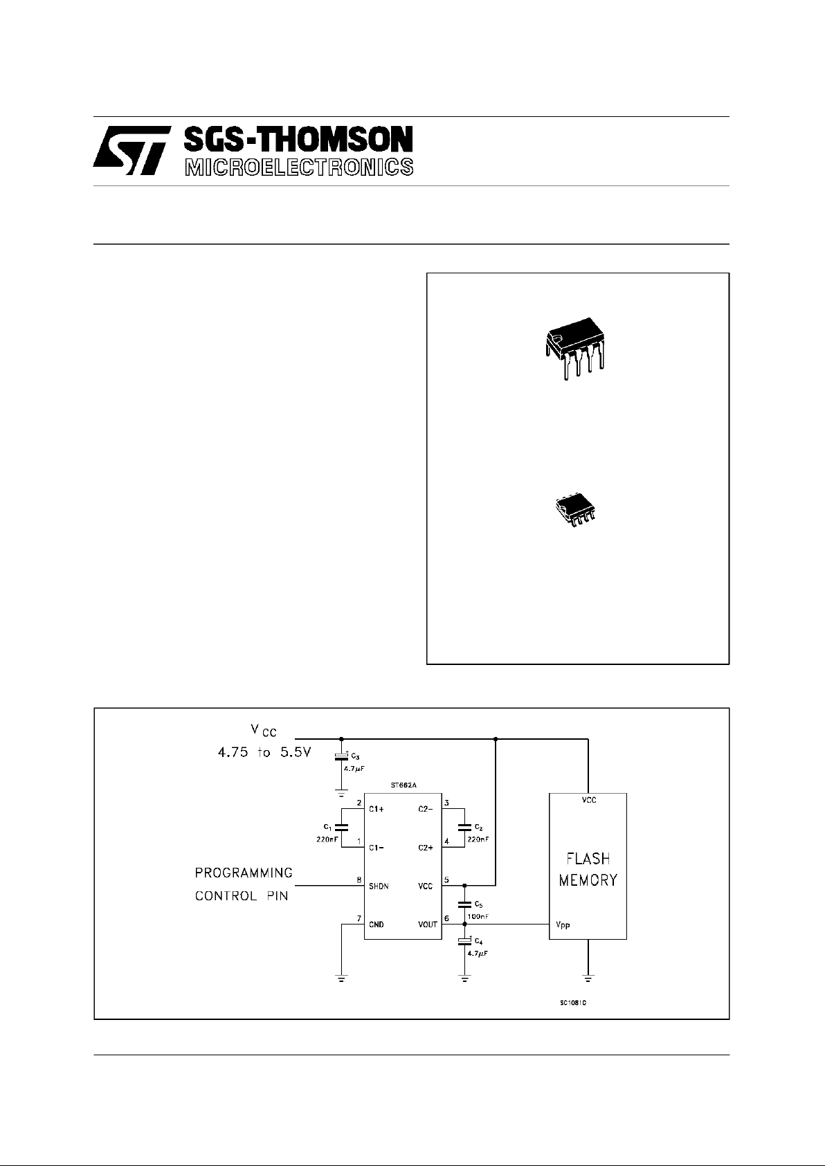
TYPICALAPPLICATION CIRCUIT
DIP-8
SO-8
1/12
ABSOLUTE MAXIMUM RATINGS
Symbol Parameter Value Unit
V
cc
DC Input Voltage to GND -0.3 to 6 V
SHDN Shutdown Voltage -0.3 to V
CC
+0.3 V
I
o
OutputCurrent Continuous 50 mA
P
tot
Power Dissipation 500 mW
T
op
Operating Ambient Temperature Range(forAC SERIES)
(for AB SERIES)
0to70
-40to85
o
C
o
C
T
stg
StorageTemperature Range - 40 to 150
o
C
Absolute Maximum Rating are those values beyond which damage to the device may occur.
Functional operation under these condition is not implied.
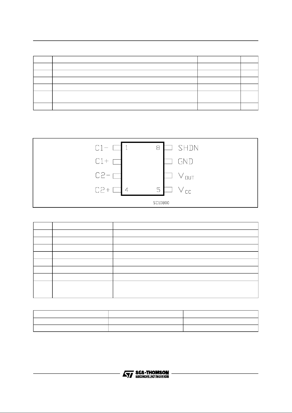
CONNECTION DIAGRAM AND (top view)
PINCONNECTIONS
Pin No Symbol Name and Function
1 C1- Negative Terminal For The FirstCharge Pump Capacitor
2 C1+ Positive Terminal For The FirstCharge Pump Capacitor
3 C2- Negative Terminal For The Second Charge Pump Capacitor
4 C2+ Positive Terminal For The SecondCharge Pump Capacitor
5V
CC
Supply Voltage
6V
OUT
12VOutputVoltage V
OUT=VCC
WheninSshutdownMode
7 GND Ground
8 SHDN ActiveHigh C-MOS logic level Shutdown Input. SHDNisinternally pulled up to
V
CC
. Connect to GND for NormalOperation. InShutdownmodethecharge
pumpsareturnedoff and V
OUT=VCC
ORDERING NUMBERS
Type DIP-8 SO-8 (*)
ST662AB ST662ABN ST662ABD
ST662AC ST662ACN ST662ACD
(*) AVAILABLE IN TAPE ANDREEL WITH ”-TR” SUFFIX
ST662A
2/12
ELECTRICAL CHARACTERISTICS (Refer to the test circuits, VCC= 4.5V to 5.5V Ta=T
min
to T
max
unless otherwisespecified. TypicalValue are referred at Ta=25oC)
Symbol Parameter Test Conditions Min. Typ. Max. Unit
V
o
OutputVoltage Io= 0mA to20 mA 11.4 12 12.6 V
V
o
OutputVoltage Io= 0 mA to30mA VCC=4.75 to 5.5V 11.4 12 12.6 V
I
Q1
Quiescent Current No Load, V
SHDN
=0 100 500 µ A
I
Q2
Shutdown Current No Load, V
SHDN=VCC
110µA
I
SH
Shutdown Pin Current V
SHDN
=0V, VCC=5V
V
SHDN=VCC
=5V
-50 -12
0
-5 µA
µA
V
il
Shutdown Input LowThreshold 0.4 V
V
ih
Shutdown Input High
Threshold
2.4 V
f
o
OscillatorFrequency VCC= 5V, Io=30 mA 400 KHz
ν Power Efficecy V
CC
= 5V, Io=30mA 72 %
R
sw
VCC-V
OUT
Switch Impedance V
SHDN=VCC
=5V, Io=100µA12KΩ
Do not overload or short the Output to Ground. If the above conditions are observerd, the device may be damaged.
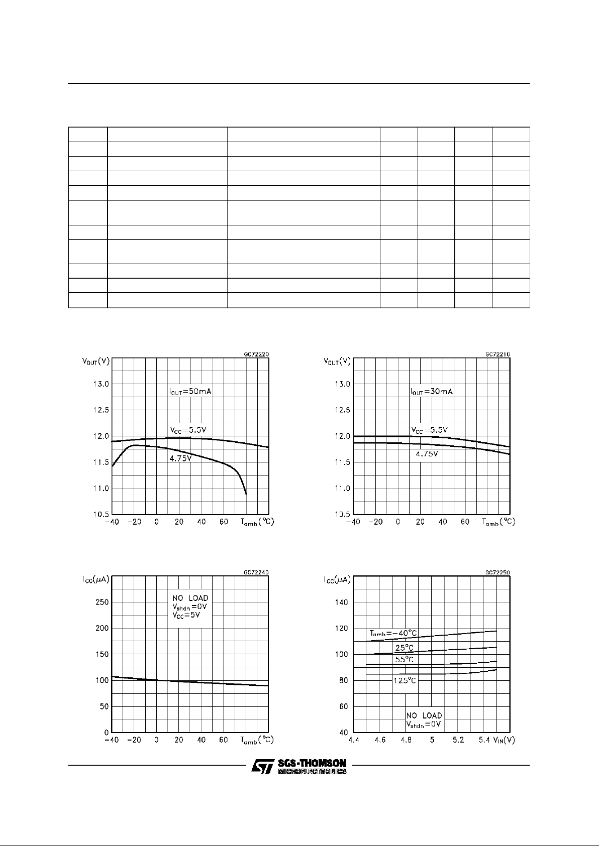
OutputVoltage vs Temperature
Supply Currentvs Temperature
OutputVoltage vs Temperature
SupplyCurrernt vs SupplyVoltage
ST662A
3/12
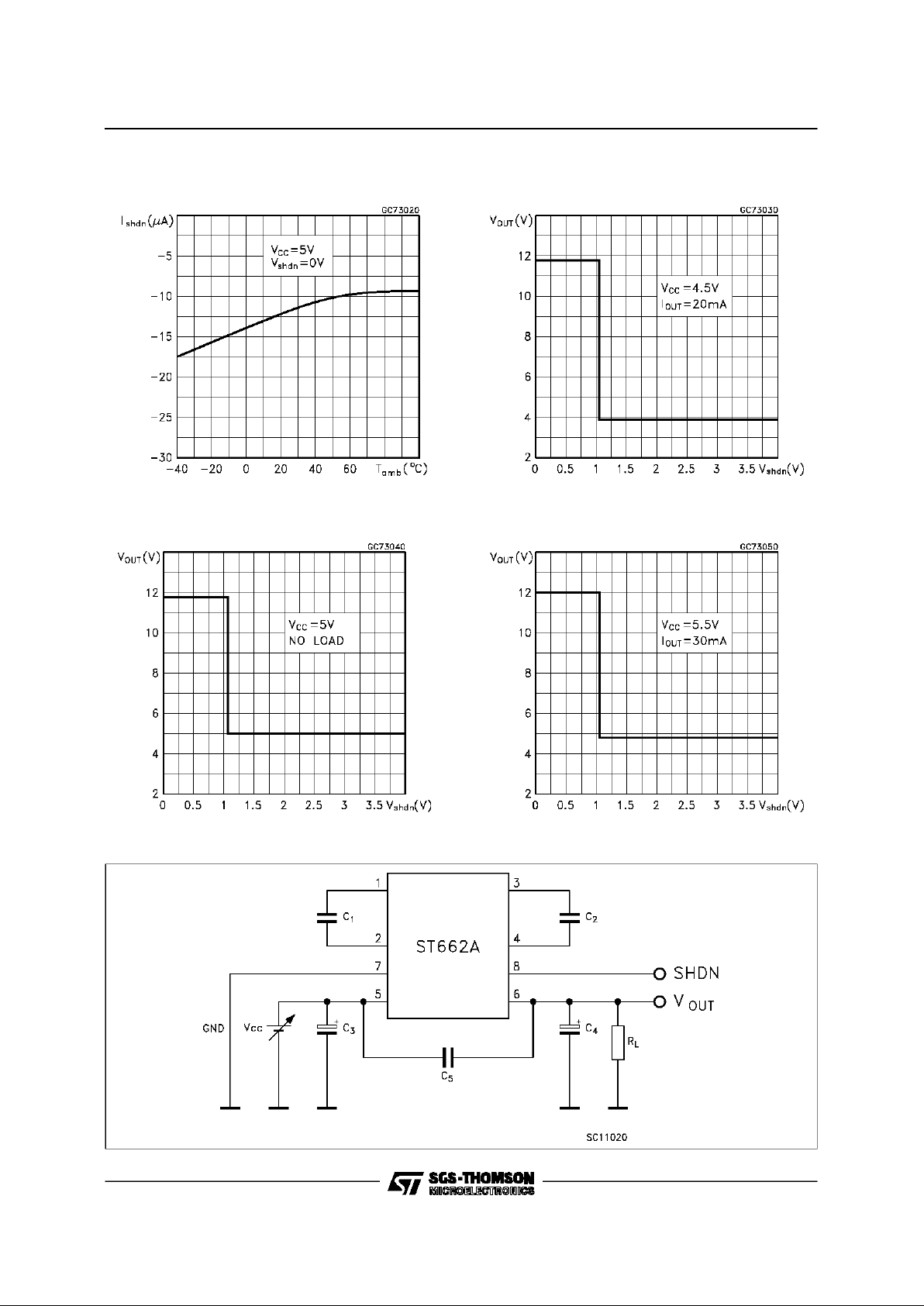
OutputVoltage vs Shutdown Input Voltage
Test Circuit
OutputVoltage vs Shutdown Input Voltage
SHDNPin Currentvs Temperature OutputVoltage vs Shutdown Input Voltage
ST662A
4/12
 Loading...