

SGS Thomson Microelectronics ST6399B1, ST6399, ST6397B1, ST6397, ST6395B1 Datasheet
...
ST6391, ST6392, ST6393
ST6395, ST6397, ST6399
DATA SHEET

USE INLIFE SUPPORTDEVICES OR SYSTEMS MUSTBE EXPRESSLYAUTHORIZED.
SGS-THOMSON PRODUCTS ARE NOT AUTHORIZED FOR USE AS CRITICAL COMPONENTS INLIFE SUPPORT DEVICES OR SYSTEMS WITHOUT THE EXPRESSWRITTEN APPROVAL OF SGS-THOMSON Microelectronics.
As used herein :
1. Life support devices or systems are those which (a) are
intended for surgical implant into the body, or (b) support
or sustain life, and whose failure to perform, when properly used in accordance with instructions for use provided with the product, can be reasonably expected to
result in significant injury to the user.
2. A criticalcomponent is any component of alife support
device or system whose failure to perform can reasonably be expected to cause the failure of the life support
device or system, or to affect its safety or effectiveness.

ST639x DATASHEET INDEX
ST6391, ST6392, ST6393
Pages
ST6395, ST6397, ST6399
GENERAL DESCRIPTION . . . . . . . . . . . . .......................... 3
PINDESCRIPTION ......................................... 5
ST639x CORE . . . . . . . . . . . . . . . . . . . . . . . . . . . . . . . . . . . . . . . . . . . . 7
MEMORYSPACES . . . . . . . . . . . . . . . . . . . . . . . . . . . . . . . . . . . . . . . . . 10
INTERRUPT . . . .......................................... 17
RESET . . . . . . . . . . . . . . . . . . . . . . . . . . . . . . . . . . . . . . . . . . . . . . . . 21
WAIT& STOPMODES . . . . . . . . . . . . . . . . ....................... 23
ON-CHIPCLOCK OSCILLATOR . . . . . . . . . . . . . . . . . . . . . . . . . . . . . . . . . . 24
INPUT/OUTPUT PORTS . . . . . . . . . . . . . . . . . . . . . . . . . . . . . . . . . . . . . . 25
TIMERS . . . . . . . . . . . . . . . . . . . . . . . . . . . . . . . . . . . . . . . . . . . . . . . 28
HARDWARE ACTIVATEDDIGITAL WATCHDOG FUNCTION . . . . . . ............. 31
SERIALPERIPHERALINTERFACE . . . . . . . . . . . . . . . . . . . . . . . . . . . . . . . . . 32
6-BITPWMD/A CONVERTERS . . . . . . . . . . . . . . . . ................... 41
AFC A/DCOMPARATOR . . . . . . . . . . . . . . . . . . . . . . . . . . . . . . . . . . . . . . 41
DEDICATED LATCHES . . . . . . . . . . . . . . . . . . . . . . . . . . . . . . . . . ...... 42
ON-SCREENDISPLAY(OSD) . . . . . ............................... 43
SOFTWARE DESCRIPTION. . . . . ................................ 52
ABSOLUTEMAXIMUMRATINGS . . . . . . . . . . . . . . . . . . . . . . . . . . . . . . . . . . 57
PACKAGEMECHANICAL DATA . . . . . . . . . . . . . . . . . . . . . . . . . . . . . . . . . . 61
ORDERINGINFORMATION TABLE . . . . . . . . . . . . . . . . . . . . . ............ 64
............................... 1

ST6391, ST6392, ST6393
FOR TV FREQUENCY SYNTHESIS WITH OSD
4.5 to6V supply operatingrange
8MHzMaximum Clock Frequency
UserProgram ROM: Upto 20140 bytes
Reserved Test ROM:Up to 340 bytes
Data ROM: User selectable size
Data RAM: 256 bytes
Data EEPROM: Up to 384 bytes
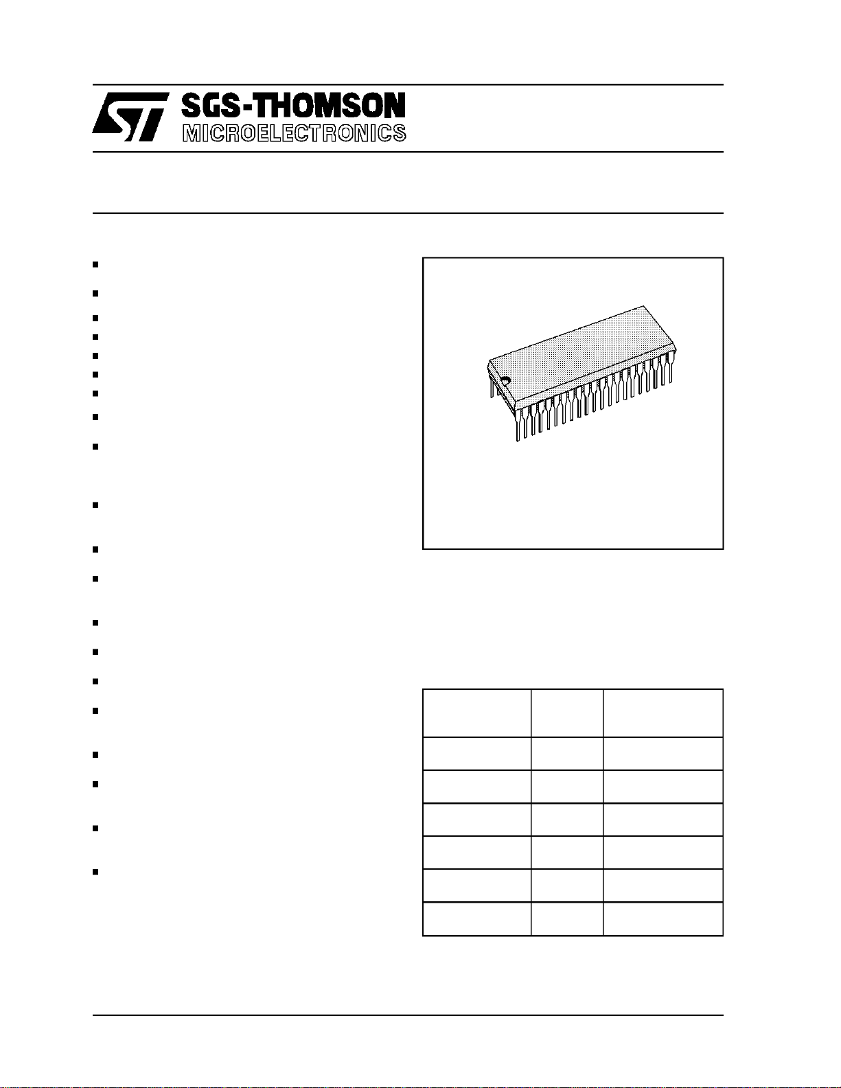
42-PinShrink Dual inLine Plastic Package
Up to 23 software programmable general pur-
pose Inputs/Outputs, including 2 direct LED
driving Outputs
Two Timerseach includingan 8-bit counter with
a 7-bitprogrammable prescaler
Digital WatchdogFunction
ST6395, ST6397, ST6399
8-BIT HCMOS MCUs
PRELIMINARY DATA
1
PSDIP42
(Ordering Information at the end of the datasheet)
Serial Peripheral Interface(SPI)supporting
S-BUS/I
2
C BUSand standardserial protocols
SPIfor externalfrequency synthesistuning
Up to Six 6-Bit PWMD/A Converters
AFCA/D converterwith 0.5V resolution
Five interrupt vectors (IRIN/NMI, Timer 1 & 2,
VSYNC,PWR INT.)
On-chipclock oscillator
5 Lines by 15 Characters On-ScreenDisplay
Generatorwith 128 Characters
All ROM types are supported by pin-to-pin
EPROMand OTP versions.
The development tool of the ST639x microcon-
trollers consists of the ST638x-EMUemulation
and development system to be connectedvia a
standard RS232 serial line to an MS-DOSPersonal Computer.
DEVICE SUMMARY
DEVICE
ST6391 16K 128
ST6392 20K 128
ST6393 16K 128
ST6395 20K 384
ST6397 20K 384
ST6399 16K 128
ROM
(Bytes)
EEPROM
(Bytes)
October 1993
This isPreliminaryinformation from SGS-THOMSON. Details are subjectto change withoutnotice.
1/64
ST6391,92,93,95,97,99
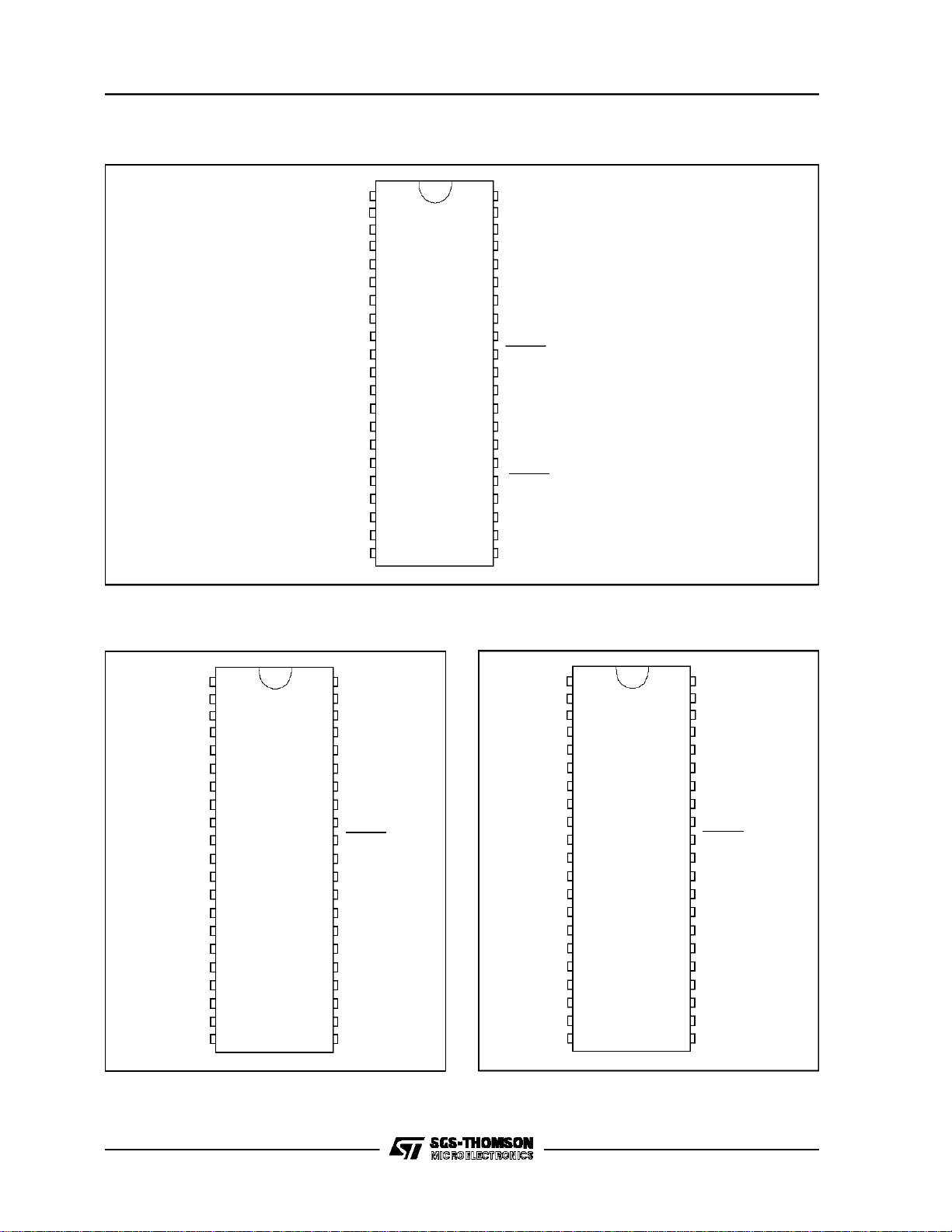
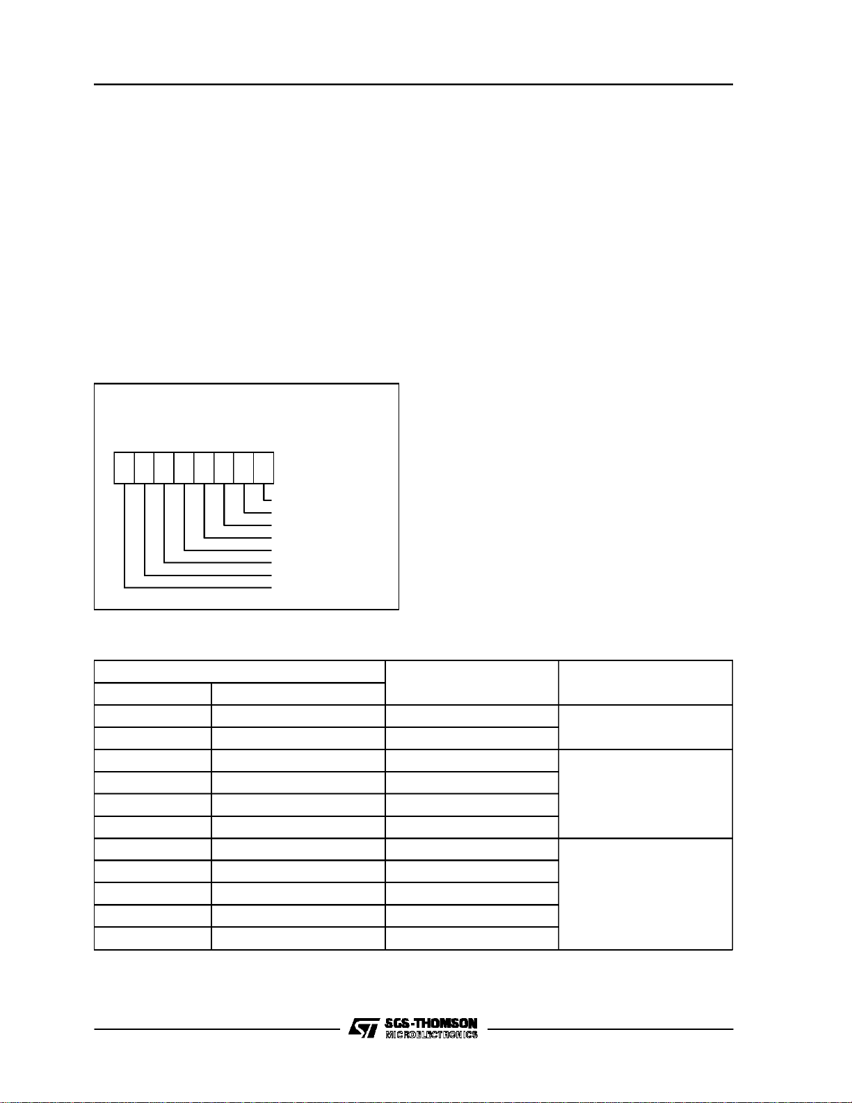
Figure1. ST6393/97 Pin Configuration
DA0
DA1
DA2
DA3
DA4
DA5
PB1
PB2
AFC
PB4
PB5
PB6
PA0
PA1
PA2
PA3
PA4
PA5
PA6
PA7
V
SS
Figure2. ST6392/99 Pin Configuration
10
11
12
13
14
15
16
17
18
19
1
2
3
4
5
6
7
8
9
20
21
V
42
41
DD
PC0 (SCL)
PC1 (SDA)40
PC2
39
PC3 (SEN)
38
37
PC4
36
PC5
35
PC6 (IRIN)
PC7
34
RESET
33
32
OSCout
31
OSCin
TEST
30
29
OSDOSCout
OSDOSCin
28
27
VSYNC
26
HSYNC
25
BLANK
B
24
23
G
22
R
VA00339
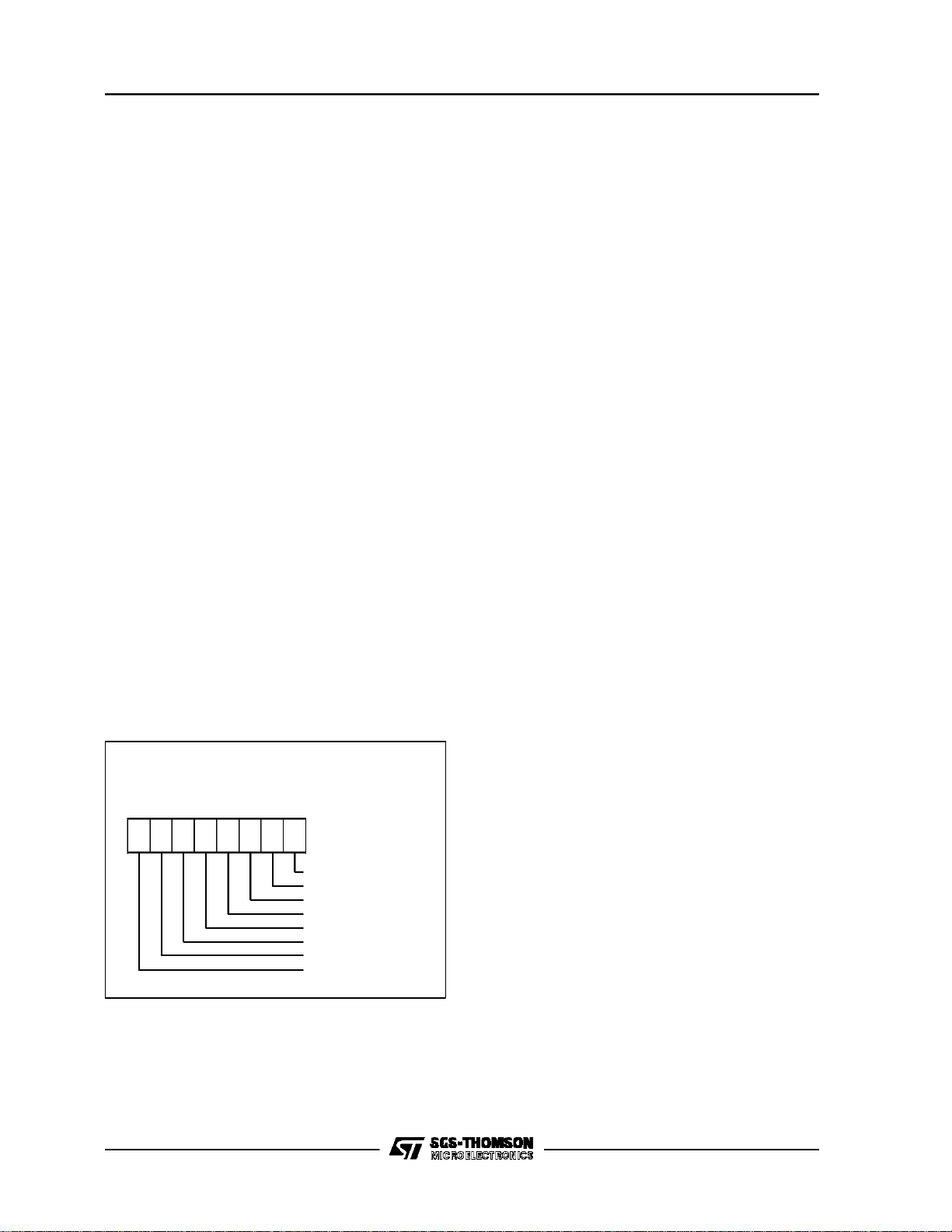
Figure3. ST6391/95 PinConfiguration
DA0
DA1
DA2
DA3 4
62.5kHz OUT
PB0
PB1
PB2
PB3
PB4
PB5
PB6
PA0
PA1
PA2
PA3
PA4
PA5
PA6 (HD0)
PA7 (HD1)
V
SS
10
11
12
13
14
15
16
17
18
19
20
21
1
2
3
5
6
7
8
9
V
42
PC0 (SCL)
41
40
PC1 (SDA)
PC2
39
PC3 (SEN)
38
37
PC4 (PWRIN)
36
PC5
PC6 (IRIN)
3435PC7
RESET
33
32
OSCout
OSCin
31
TEST
30
29
OSDOSCout
OSDOSCin
28
27
VSYNC
26
HSYNC
25
BLANK
B
24
23
G
22
R
DD
VA00340
Note 1.ST6395 only
DA0
DA1
DA2
DA3 4
PB0
PB1
PB2
PB3
PB4
PB5
PB6
PA0
PA1
PA2
PA3
PA4
PA5
PA6 (HD0)
PA7 (HD1)
1
2
3
5DA4
6
7
8
9
10
11
12
13
14
15
16
17
18
19
20
V
21
SS
V
42
41
DD
PC0 (SCL)
PC1 (SDA)40
PC2
39
PC3 (SEN)
38
37
PC4 (PWRIN )
36
PC5
PC6 (IRIN)
3435PC7
RESET
33
OSCout
32
OSCin
31
TEST
30
29
OSDOSCout
OSDOSCin
28
27
VSYNC
26
HSYNC
BLANK
25
B
24
G
23
22
R
(1)
VA00337
2/64

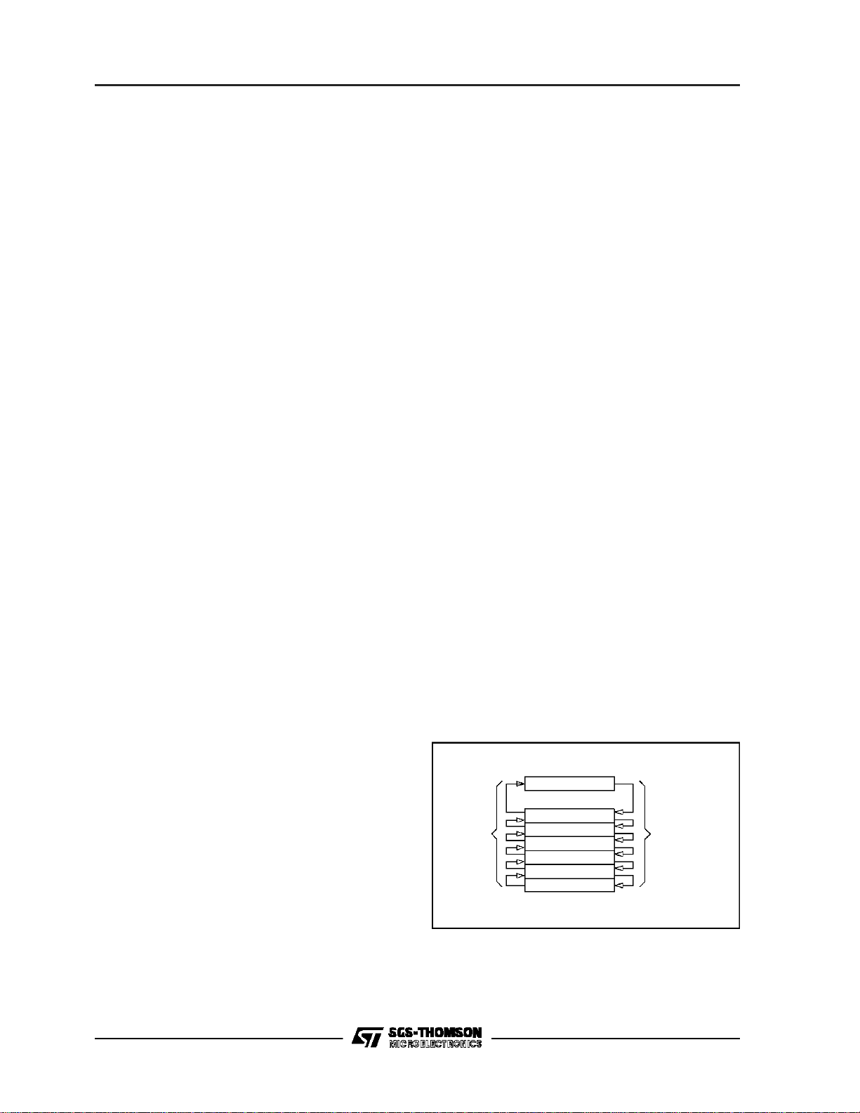
GENERAL DESCRIPTION
The ST639xmicrocontrollersaremembersof the 8bit HCMOS ST638xfamily,a seriesof devicesspeciallyorientedto TVapplications.DifferentROMsize
and peripheral configurationsare available to give
the maximum application and cost flexibility. All
ST639xmembersare basedon a building blockapproach:a commoncoreissurroundedbya combination of on-chip peripherals (macrocells) available
from a standardlibrary. These peripheralsare designedwith the same Coretechnologyprovidingfull
compatibility and short design time. Many of these
macrocells are specially dedicated to TV applications.The macrocellsof the ST639xfamily are:two
Timer peripherals each including an 8-bit counter
with a 7-bit software programmable prescaler
ST6391,92,93,95,97,99
(Timer), a digital hardware activated watchdog
function(DHWD), a 14-bitvoltage synthesis tuning
peripheral, a Serial Peripheral Interface (SPI), up
to six 6-bit PWMD/A converters,an AFC A/D converter with 0.5V resolution, an on-screen display
(OSD)with 15charactersper line and 128 characters (in two banks each of64 characters).In addition the followingmemory resourcesare available:
programROM (up to 20K), data RAM (256 bytes),
EEPROM(up to 384 bytes).Refer to pin configurations figures and to ST639x device summary (Table 1) for the definition of ST639x family members
and a summaryof differencesamong the different
types.
3/64

ST6391,92,93,95,97,99
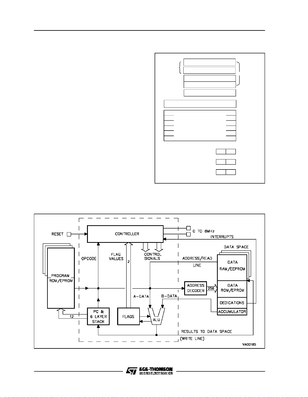
Figure4. ST6391,92,93,95,97,99Block Diagram
* Refer To Pin Configuration For Additional Information
TEST
IRIN/PC6
TEST
IR INTERRUPT
Input
DATA ROM
USER PROGRAM
ROM
UP TO 20 kBytes
USER SELECTABLE
DATA RAM
256 Bytes
DATA EEPROM
384 Bytes
PC
STACK LEVEL 1
STACK LEVEL 2
STACK LEVEL 3
STACK LEVEL 4
STACK LEVEL 5
STACK LEVEL 6
8-BIT CORE
POWER SUPPLY OSCILLATOR RESET
V
DD
V
SS
OSCin OSCout
RESET
PORT A
PORT B
PORT C
SERIAL PERIPHERAL
INTERFACE
TIMER 1
TIMER 2
DIGITAL
WATCHDOG/TIMER
D/AOutputs
AFC Input
ON-SCREEN
DISPLAY
PA0 - PA7 *
PB0 - PB7 *
PC2, PC4 - PC7 *
PC0 / SCL
PC1 / SDA
PC3 / SEN
DA0 - DA5
AFC
R, G, B, BLANK
HSYNC, VSYNC
VR01753G
Table 1. Device Summary
DEVICE
ST6391 16K 256 128 NO 5 3 NO NO 62.5 NO ST63E91
ST6392 20K 256 128 NO 4 3 YES YES 62.5 YES ST63E92
ST6393 16K 256 128 YES 6 3 NO NO 62.5 NO ST63E93
ST6395 20K 256 384 NO 5 3 NO YES 100 NO ST63E95
ST6397 20K 256 384 YES 6 3 NO NO 100 NO ST63E97
ST6399 16K 256 128 NO 4 3 YES YES 62.5 YES ST63E99
ROM
(Bytes)
RAM
(Bytes)
EEPROM
(Bytes)
AFC D/A
COLOUR
PINS
LOW
POWER IN
RESET
PWRIN
PIN
4/64
SPI
CLK FREQ.
(kHz)
62.5kHz
Pin
EMULATING
DEVICES

PIN DESCRIPTION
V
andVSS. Power issupplied to the MCU using
DD
these twopins. V
ispower and VSSistheground
DD
connection.
OSCin, OSCout. These pins are internally con-
nected to the on-chip oscillator circuit. A quartz
crystal or a ceramic resonator can be connected
between these two pins in order to allow the correct operation of the MCU with various stability/cost trade-offs. The OSCin pin is the input pin,
the OSCoutpin is the output pin.
RESET. The activelow RESET pin is used to start
the microcontrollerto the beginning ofits program.
Additionally the quartz crystal oscillator will be disabled when theRESET pin islow to reduce power
consumptionduringresetphase (ST6392/99only).
TEST. The TESTpin must be held at V
SS
for nor-
mal operation.
PA0-PA7. These 8 linesare organizedas one I/O
port (A). Eachline may be configuredas either an
input withor withoutpull-upresistor oras an output
under softwarecontrol of the datadirectionregister. PinsPA4 toPA7 are configured as open-drain
outputs (12V drive). On PA4-PA7 pins the input
pull-up option is not available while PA6 and PA7
have additional current driving capability (25mA,
:1V).PA0 to PA3pins areconfiguredas push-
V
OL
pull.
PB0-PB2, PB4-PB6. These 6 linesare organized
as one I/O port (B).Each line may be configuredas
either aninput withorwithoutinternalpull-up resistor or as an output under software control of the
data directionregister.
PC0-PC7. These 8 linesare organizedas one I/O
port (C). Each line may be configured as either an
input with or without internal pull-up resistor or as
an output under software control of the data direction register. Pins PC0 to PC3 are configured as
open-drain(5V drive)in output mode while PC4 to
PC7 are open-drain with 12V drive and the input
pull-up options doesnotexist on thesefour pins.
PC0, PC1 and PC3 lines when in output mode are
“ANDed” with the SPI control signals and are all
ST6391,92,93,95,97,99
Open-drain.PC0is connectedtothe SPI clock signal (SCL), PC1 with the SPI data signal (SDA)
while PC3 is connected with SPI enable signal
(SEN, used inS-BUS protocol).Pin PC4 and PC6
can also be inputstosoftwareprogrammableedge
sensitive latches which can generate interrupts;
PC4 can be connected to Power Interrupt while
PC6 can be connected to the IRIN/NMI interrupt
line.
DA0-DA5. These pins are the six PWM D/A outputs of the 6-bit on-chip D/A converters. These
lines have open-drain outputs with 12V drive. The
output repetition rate is 31.25KHz (with 8MHz
clock).
AFC.This is the input ofthe on-chip 10 levels comparator that can be used to implement the AFC
function. This pin is an high impedance input able
to withstand signals with a peak amplitude up to
12V.
OSDOSCin, OSDOSCout. These are the On
Screen Display oscillator terminals. An oscillation
capacitorand coil network have tobeconnected to
provide theright signal to theOSD.
HSYNC, VSYNC. These are the horizontal and
vertical synchronizationpins. The activepolarity of
these pins to the OSD macrocell can be selected
by the user as ROM mask option. If the device is
specified to have negative logic inputs, then these
signals are lowthe OSD oscillator stops. If the device is specifiedto have positivelogic inputs,then
when these signals are high the OSD oscillator
stops.
R, G, B, BLANK. Outputsfrom the OSD. R, G and
B are thecolor outputs while BLANK is the blanking output.All outputsare push-pull. The activepolarity of these pins can be selected by the user as
ROM mask option.
62.5kHz OUT. This pin is available only on the
ST6392/99. The pin isan open drain (12V) output
at the frequencyof 62.5kHz (with an 8MHz clock).
The pin can be used to drive the SGS-THOMSON
TEA5640 Chroma Processor. Refer to the
TEA5640 Data sheetfor more information.
5/64
ST6391,92,93,95,97,99
Table 2. Pin Summary
Pin Function Description
DA0 to DA5 Output, Open-Drain, 12V
AFC Input, High Impedance, 12V
R,G,B, BLANK Output, Push-Pull
HSYNC, VSYNC Input, Pull-up, Schmitt Trigger
OSDOSCin Input, High Impedance
OSDOSCout Output, Push-Pull
TEST Input, Pull-Down
OSCin Input, Resistive Bias, Schmitt Trigger to Reset Logic Only
OSCout Output, Push-Pull
RESET Input,Pull-up, Schmitt Trigger Input
PA0-PA3 I/O, Push-Pull, Software Input Pull-up, Schmitt Trigger Input
PA4-PA5 I/O, Open-Drain, 12V,No Input Pull-up, Schmitt Trigger Input
PA6-PA7 I/O, Open-Drain, 12V,No Input Pull-up, Schmitt Trigger Input, High Drive
PB0-PB6 I/O, Push-Pull, Software Input Pull-up, Schmitt Trigger Input
PC0-PC3 I/O, Open-Drain,5V , Software Input Pull-up, Schmitt Trigger Input
PC4-PC7 I/O, Open-Drain,12V, No Input Pull-up, Schmitt Trigger Input
V
DD,VSS
Power Supply Pins
62.5kHz OUT Output, Open-Drain 12V
6/64
ST6391,92,93,95,97,99
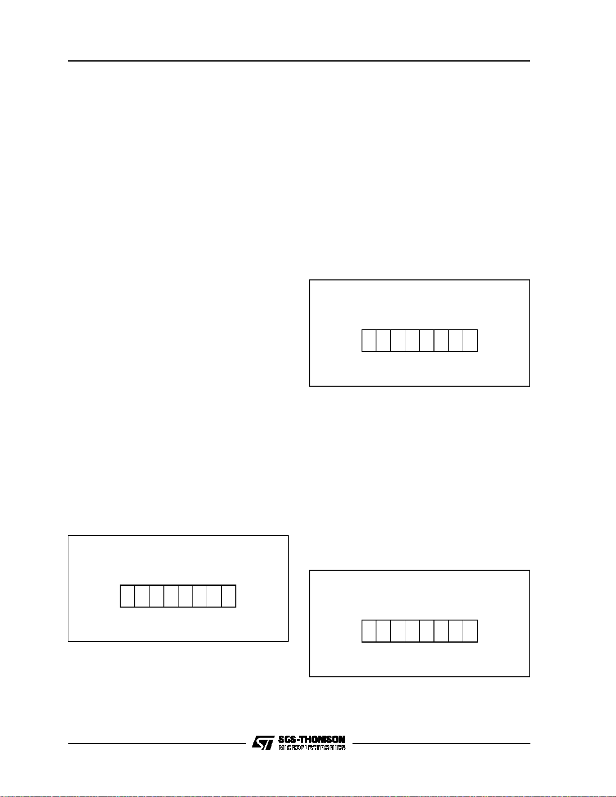
ST639x CORE
TheCoreoftheST639xFamilyisimplementedindependently from the I/O or memory configuration.
Consequently,it can be treated as an independent
centralprocessorcommunicatingwithI/Oandmemoryvia internaladdresses,data,andcontrolbusses.
The in-core communication is arrangedas shown
in the followingblock diagram figure; the controller
being externallylinkedto both thereset and the oscillator, while the core is linked to thededicatedonchip macrocells peripherals via the serial data bus
and indirectly for interrupt purposes through the
control registers.
Registers
The ST639x Family Core has five registers and
three pairs of flags available to the programmer.
They are shown in Figure 5 and are explained in
the following paragraphs together with the program and data memorypage registers.
Accumulator(A). Theaccumulatorisan 8-bitgeneral purpose registerused in allarithmetic calculations, logical operations, and data manipulations.
Theaccumulatoris addressedin thedataspaceas
RAMlocationat theFFhaddress.
Accordingly, the ST639x instruction set can use
the accumulator as any other register of the data
space.
Figure6. ST639x Core Programming Model
INDEX
REGISTER
PROGRAMCOUNTER
NORMAL FLAGS
INTERRUPT FLAGS
NMI FLAGS
b7
X REG.POINTER
b7
Y REG.POINTER
V REGISTER
b7
b7
W REGISTER
b7
ACCUMULATOR
SIX LEVELS
STACKREGISTER
b0
SHORT
DIRECT
b0
ADDRESSING
MODE
b0
b0
b0
b0b11
C
Z
C
Z
C
Z
VA000423
Figure5. ST639x Core Block Diagram
7/64
ST6391,92,93,95,97,99
ST639x CORE (Continued)
Indirect Registers (X, Y). These two indirect reg-
istersare usedas pointers tothe memorylocations
in the dataspace. They are usedin theregister-indirect addressing mode.These registers can be
addressed in the data space as RAM locations at
the 80h (X)and 81h (Y)addresses.They can also
be accessed with the direct, short direct, or bit direct addressing modes. Accordingly, the ST639x
instructionsetcan use the indirect registers as any
other registerof the data space.
Short Direct Registers (V, W). These two registers are used to save one byte in short direct addressing mode.These registerscan be addressed
in the data space as RAM locations atthe 82h (V)
and 83h (W) addresses. They can also be accessed with the direct and bit direct addressing
modes. Accordingly, the ST639x instruction set
can use the shortdirect registers as any other register ofthe data space.
Program Counter (PC)
Theprogramcounterisa12-bitregisterthatcontains
the address of the next ROM location to be processed bythecore.ThisROMlocationmaybe anopcode, an operand, or an address of operand. The
12-bit length allows the direct addressing of 4096
bytesin theprogramspace.Nevertheless,iftheprogramspacecontainsmorethan4096 locations,the
further programspace can be addressed by using
the ProgramROM Page Register. The PC value is
incremented, after it is read for the address of the
currentinstruction,bysendingitthroughtheALU,so
giving the address of the next bytein the program.
Toexecuterelative jumpsthe PC and the offsetvaluesare shiftedthroughtheALU, where they will be
added,andtheresultisshiftedbackintothePC.The
program counter can be changed in the following
ways:
JP (Jump)instruction....PC=Jump address
CALL instruction...........PC=Call address
Relative Branch
instructions...................PC=PC+offset
Interrupt........................PC=Interruptvector
Reset............................PC=Resetvector
RET &RETI instructions............PC=Pop (stack)
Normal instruction........PC=PC+1
Flags (C, Z)
The ST639x Core includesthree pairsof flags that
correspond to 3 differentmodes: normalmode,interrupt mode and Non-Maskable-Interrupt-Mode.
Each pair consistsof a CARRY flag and a ZERO
flag. One pair (CN, ZN) is used duringnormal operation, one pair is used during the interruptmode
(CI,ZI)andone is usedduring thenot-maskableinterruptmode (CNMI, ZNMI).
The ST639x Cor e uses the pair of flags that correspondsto the actual mode: as soon as an inter rupt
(resp. a Non-M as kable-Interrupt) is generated, the
ST639xCoreusesthe interrupt flags(resp. the NMI
flags)insteadof the normalflags. When theRETI instruc ti onisexecuted,thenormalflags(re sp.the interruptflags)arerestoredif theMCUwasin the normal
mode(res p.intheinterr uptmode)beforetheinterr upt.
Shouldbeobservedthateachflagsetcanonly be addressed in its own routine (Not-maskable interrupt,
normal interrupt or main routine). The interrupt flags
arenot cleared during the context switching and so,
theyremain in thestate they wereatthe exitof the last
routineswit ching.
The Carry flag is set when a carry or a borrow occurs during arithmetic operations, otherwise it is
cleared. The Carry flag is also set to the value of
the bit tested in a bit test instruction, and participates in the rotate left instruction.
TheZeroflagissetif theresultofthelastarithmetic
or logical operation wasequal to zero, otherwise it
is cleared.
The switching between these three sets is automaticallyperformedwhen anNMI,an interrupt and
a RETI instructions occur. As the NMI mode is
automatically selected after the reset ofthe MCU,
the ST639xCore uses atfirst the NMI flags.
Figure7. Stack Operation
PROGRAM COUNTER
WHEN
RET OR RETI
OCCURS
STACK LEVEL 1
STACK LEVEL 2
STACK LEVEL 3
STACK LEVEL 4
STACK LEVEL 5
STACK LEVEL 6
WHEN CALL
OR
INTERRUPT REQUEST
OCCURS
VA000424
8/64
ST639x CORE (Continued)
Stack
The ST639x Core includes true LIFO hardware
stack that eliminatesthe need for a stack pointer.
The stackconsists of six separate 12-bit RAM locations that do notbelong to the data space RAM
area. When a subroutine call (or interruptrequest)
occurs,the contentsofeachlevelis shiftedinto the
next levelwhile the contentofthe PC is shiftedinto
the first level (the value of the sixth level will be
lost). When subroutine or interrupt return occurs
(RET or RETI instructions),thefirst level registeris
shifted back into the PCand thevalue of eachlevel
is shifted back into the previous level. These two
operating modes are describedin Figure 7. Since
the accumulator,as all otherdata space registers,
is notstored inthisstack the handlingof thisregisters shall be performed inside the subroutine. The
stack pointer will remain in its deepest position,if
more than 6 calls or interrupts are executed, so
that the last return address will be lost. It will also
remain in its highest position if the stack is empty
and a RET or RETI is executed. In this case the
next instructionwill be executed.
Memory Registers
The PRPR can be addressed like a RAM location
in the Data Space at the CAh address; nevertheless it is a write-only register that can not be accessed with single-bit operations.This register is
used to select the 2-Kbyte ROM bank of the Program Spacethat will be addressed.The number of
the pagehastobe loaded inthePRPR.ThePRPR
is not cleared during the MCU initialization and
should thereforebe defined before jumpingout of
the static page. Refer to the Program Space description for additional information concerning the
use of this register. The PRPR is not modified
when an interruptor a subroutine occurs.
Figure8. Program ROMPage Register
PRPR
Program ROMPage Register
(CAh, Write Only)
D7 D6 D5 D4 D3 D2 D1 D0
ST6391,92,93,95,97,99
The DRBR can be addressedlike a RAMlocation
in the Data Space at the E8h address, nevertheless it is write-only register that can not be accessed with single-bit operations. This register is
used to select the desired 64-byteRAM/EEPROM
bank of the Data Space. The numberof the bank
has to be loaded inthe DRBR and the instruction
has to point to the selected location as itwas inthe
0 bank (from 00h address to 3Fh address). This
register is undefined afterReset. Refer to the Data
Space description for additional information. The
DRBRregisterisnot modifiedwhen a interruptor a
subroutine occurs.
Figure9. Data RAM Bank Register
DRBR
Data RAM Bank Register
(E8h, Write Only)
D7 D6 D5 D4 D3 D2 D1 D0
TheDRWR registercanbeaddressedlike a RAMlocationin theDataSpaceat the C9haddress,nevertheless it is write-only register that can not be
accessed with single-bit operations.This register is
used to move up and down the 64-byte read-only
datawindow (fromthe 40h addressto 7Fh address
of the Data Space)along the ROM of the MCU by
stepof 64 bytes.Theeffectiveaddressof thebyteto
bereadasadata inthe ROMisobtainedby the concatenationofthe6lesssignificantbitsoftheaddress
given in the instruction(as less significant bits)and
the contentof the DRWR (as most significantbits).
RefertotheDataSpacedescriptionforadditionalinformation.
Figure10. Data ROM Window Register
DRWR
Data ROM Window Register
(C9h, Write Only)
D7 D6 D5 D4 D3 D2 D1 D0
9/64

ST6391,92,93,95,97,99
MEMORY SPACES
The MCUs operate in three different memory
spaces: Stack Space, Program Space, and Data
Space. A descriptionof these spaces is shown in
Figure 11.
Stack Space
Thestack spaceconsistsof six 12 bit registers that
areusedfor stackingsubroutineandinterrupt return
addressesplusthecurrentprogramcounterregister.
Program Space
The program space is physically implemented in
the ROM and includes all the instructions that are
to be executed, as well as the data requiredforthe
immediate addressing mode instructions, the reserved test area and uservectors. It is addressed
thanks to the 12-bit Program Counter register (PC
register) and so, the ST639x Core can directlyaddress upto 4K bytesof Program Space.Nevertheless, the ProgramSpace can be extended by the
addition of 2-KbyteROM banks as it is shown in
Figure 13 in which a 20K bytes memory is described.Thesebanks areaddressed bypointing to
the 000h-7FFh locations of the Program Space
thanks to the Program Counter, andby writingthe
appropriatecode in theProgram ROM Page Register (PRPR) located at the CAh address of the
Data Space.Becauseinterruptsand common subroutines should be available all the time only the
lower 2K byte of the 4K program space are bank
switched while the upper 2K byte can be seen as
static space. Table 3 gives thedifferent codes that
allows the selection of the corresponding banks.
Note that,fromthe memory point of view,thePage
1 and the StaticPage represent the same physical
memory:it isonly adifferentway ofaddressingthe
same location. On the ST6392,95,97, a total of
2048, bytes of ROM have been implemented;
20140 areavailableas userROMwhile 340arereservedfor testing.
Figure12. ST639x 20K Bytes Program Space
AddressingDescription
Program
counter
space
0FFFh
0800h
07FFh
0000h
0000h 4FFFh
Static Page
Page 1
Page 0
Page 1
Static Page
Page 9
Figure11. ST639x Memory Addressing Description Diagram
STACK SPACE
0000h
PROGRAM COUNTER
STACK LEVEL1
STACK LEVEL2
STACK LEVEL3
STACK LEVEL4
STACK LEVEL5
STACK LEVEL6
07FFh
0800h
0FF0h
0FFFh
PROGRAM SPACE
ROM
ROM
INTERRUPT &
RESET VECTORS
0-63
000h
03Fh
040h
070h
080h
081h
082h
083h
084h
0C0h
0FFh
DATA SPACE
RAM / E EPROM
BANKING AREA
DATA ROM
WINDOW
X RE GISTER
Y R EGISTER
V RE GISTER
WREGISTER
RAM
DATA ROM
WINDOW SELECT
DATA RAM
BANK SELECT
ACCUMULATOR
VR001568
10/64
MEMORY SPACES(Continued)
Figure13. Program ROM Page Register
PRPR
Program ROMPage Register
(CAh, Write Only)
D7 D6 D5 D4 D3 D2 D1 D0
PRPR0
PRPR1
PRPR2
PRPR3
UNUSED
ST6391,92,93,95,97,99
interrupt driver in a (minor) part in the static page
(start and end), and in the second (major) part in
one dynamicpage. If it is impossible to avoid the
writing of this register in interrupts drivers, an image of this register must be saved in a RAMlocation, and eachtime theprogramwrites the PRPRit
writes also the image register.The image register
must be written first, so if an interruptoccurs between the two instructions the PRPR is not affected.
Table 3. ST639x ProgramROM Page Register
Coding
D7-D5. These bits are not used.
PRPR4-PRPR0. These are the program ROM
banking bits and thevalue loaded selects the corresponding page to be addressedin the lower part
of 4Kprogramaddress spaceas specifiedin Table
3. Thisregisteris undefined onreset.
Note. The number of bits implemented depends
on the size of the ROM of the device. Only the
lower part of address space has been bankswitched because interrupt vectors and common
subroutines should beavailable all the time. The
reason of this structure is due to the fact that it is
not possible to jump from a dynamic page to another, unless jumping back to the static page,
changingcontents of PRPR,and, than,jumping to
a differentdynamic page.
Care is required when handlingthe PRPR as it is
write only. For this reason, it is not allowed to
change the PRPR contents while executing interrupts drivers, as the driver cannot save and than
restore its previous content. Anyway, this operation may be necessaryif the sum ofcommonroutines and interrupt drivers will take more than 2K
bytes;in thiscase could benecessaryto dividethe
PRPR3 PRPR2 PRPR1 PRPR0 PC11
XXXX1
00000Page 0
00010
00100Page 2
00110Page 3
01000Page 4
01010Page 5
01100Page 6
01110Page 7
10000Page 8
10010Page 9
Memory
Page
Static
Page
(Page 1)
Page 1
(Static
Page)
11/64
ST6391,92,93,95,97,99
MEMORY SPACES(Continued)
Table 4. ST639x Program ROM Map (up to 20K Bytes)
ROM Page Device Address Description
PAGE 0
PAGE 1
“STATIC”
PAGE 2
PAGE 3
PAGE 4
PAGE 5
PAGE 6
PAGE 7
PAGE 8
0000h-007Fh
0080h-07FFh
0800h-0F9Fh
0FA0h-0FEFh
0FF0h-0FF7h
0FF8h-0FFBh
0FFCh-0FFDh
0FFEh-0FFFh
0000h-000Fh
0010h-07FFh
0000h-000Fh
0010h-07FFh
0000h-000Fh
0010h-07FFh
0000h-000Fh
0010h-07FFh
0000h-000Fh
0010h-07FFh
0000h-000Fh
0010h-07FFh
0000h-000Fh
0010h-07FFh
Reserved
User ROM
User ROM
Reserved
Interrupt Vectors
Reserved
NMI Vector
Reset Vector
Reserved
User ROM
Reserved
User ROM
Reserved
User ROM
Reserved
User ROM
Reserved
User ROM
Reserved
User ROM (End of 16KST6391,93,99)
Reserved
User ROM
PAGE 9
12/64
0000h-000Fh
0010h-07FFh
Reserved
User ROM (End of 20KST6392,95,97)

MEMORY SPACES(Continued)
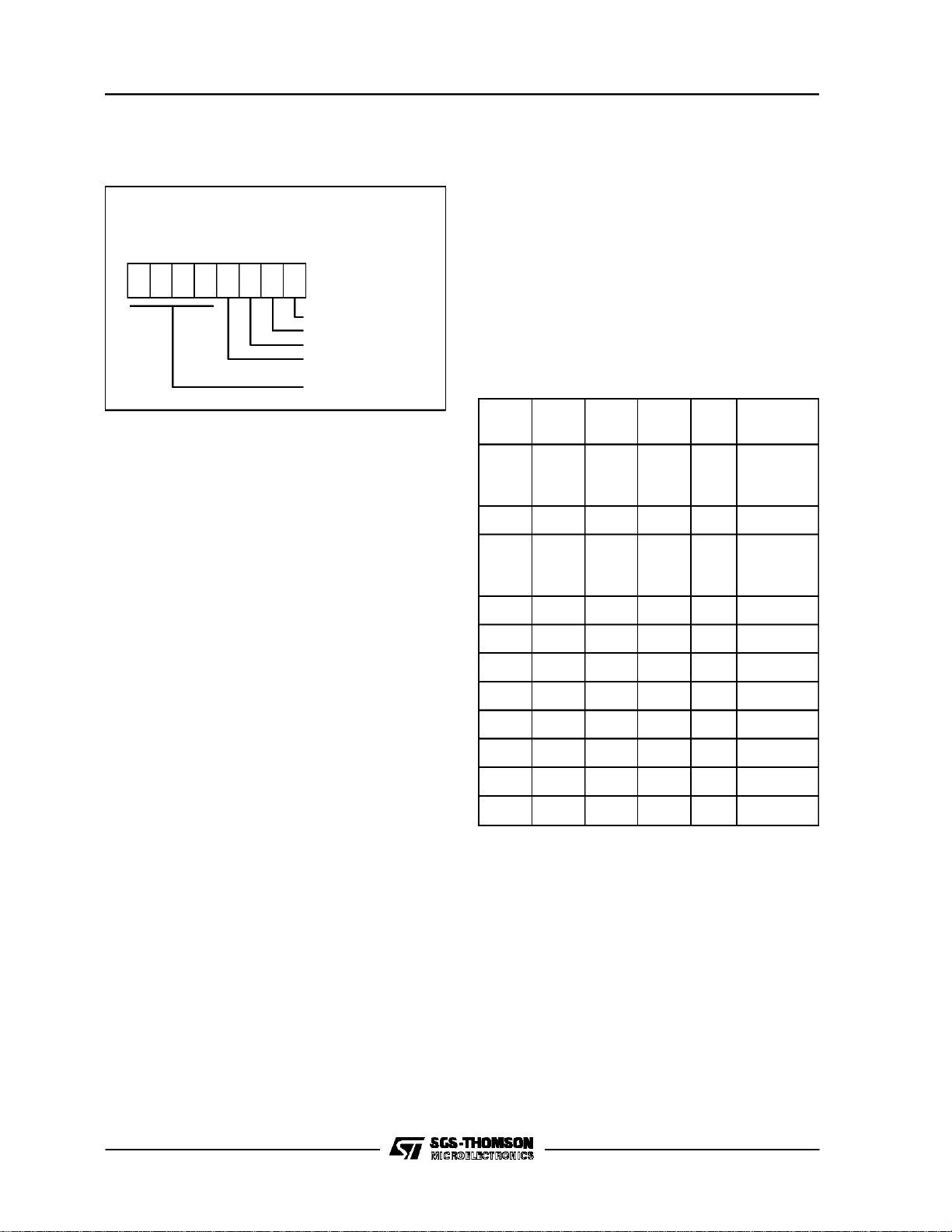
Data Space
The instruction set of the ST639x Core operates on a specific space, named Data Space
that contains all the data necessary for the
processing of the program. The Data Spaceal-
ST6391,92,93,95,97,99
lows the addressing of RAM (256 bytes for the
ST639x family), EEPROM (up to 384 bytes),
ST639xCore/peripheralregisters,andread-only
datasuch asconstantsand thelook-uptables.
Figure14. ST639x Data Space
b7 b0
DATA RAM/EEPROM/OSD
BANK AREA
DATA ROM
WINDOW AREA
X REGISTER 080h
Y REGISTER 081h
V REGISTER 082h
W REGISTER 083h
DATA RAM
PORT ADATAREGISTER 0C0h
PORT BDATAREGISTER 0C1h
PORT CDATA REGISTER 0C2h
RESERVED 0C3h
PORT ADIRECTION REGISTER 0C4h
PORT BDIRECTION REGISTER 0C5h
PORT CDIRECTION REGISTER 0C6h
RESERVED 0C7h
INTERRUPT OPTION REGISTER 0C8h
DATA ROM WINDOW REGISTER 0C9h
PROGRAM ROM PAGE REGISTER 0CAh
RESERVED 0CBh
SPI DATAREGISTER 0CCh
RESERVED
TIMER 1PRESCALER REGISTER 0D2h
TIMER 1 COUNTER REGISTER 0D3h
TIMER1 STATUS/CONTROL REG. 0D4h
RESERVED
WATCHDOG REGISTER 0D8h
000h
03Fh
040h
07Fh
084h
0BFh
0CDh
0D1h
0D5h
0D7h
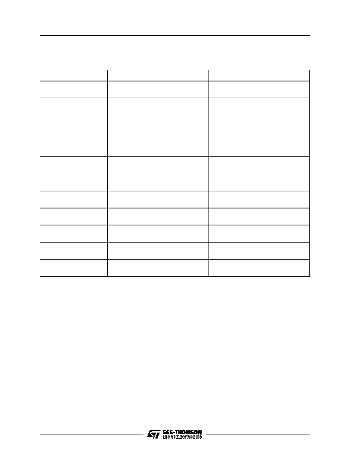
Figure15. ST639x Data Space (Continued)
b7 b0
RESERVED 0D9h
TIMER 2 PRESCALER REGISTER 0DAh
TIMER2 COUNTER REGISTER 0DBh
TIMER 2STATUSCONTROL REG. 0DCh
0DDh
RESERVED
0DFh
DA0 DATA/CONTROL REGISTER 0E0h
DA1 DATA/CONTROL REGISTER 0E1h
DA2 DATA/CONTROL REGISTER 0E2h
DA3 DATA/CONTROL REGISTER 0E3h
AFC, IR & OSD RESULT REGISTER 0E4h
OUTPUTS CONTROL REGISTER 0E5h
DA4 DATA/CONTROL REGISTER 0E6h
DA5 DATA/CONTROL REGISTER 0E7h
DATA RAM BANK REGISTER 0E8h
DEDIC. LATCHES CONTROL REG. 0E9h
EEPROMCONTROL REGISTER 0EAh
SPICONTROL REGISTER 1 0EBh
SPICONTROL REGISTER 2 0ECh
OSD CHARAC. BANK SELECT REG. 0EDh
0F0h
RESERVED
0FEh
ACCUMULATOR 0FFh
OSDCONTROLREGISTERSLOCATED
IN PAGE6 OFBANKED DATA RAM
VERTICAL START ADDRESS REG. 010h
HORIZONTALSTARTADDRESSREG. 011h
VERTICAL SPACE REGISTER 012h
HORIZONTAL SPACEREGISTER 013h
BACKGROUND COLOUR REGISTER 014h
GLOBAL ENABLEREGISTER 017h
13/64

ST6391,92,93,95,97,99
MEMORY SPACES(Continued)
Data ROM Addressing. Allthe read-onlydata ar e
physic allyimplem entedin theROM inwhich theProgramSpaceisalsoimplemented.TheROMtherefore
containstheprogramto beexecutedandalsotheconstantsandthelook-uptablesneededforthe program.
Thelocat i onsofDataSpaceinwhichthedifferentconstants and look-up tables are addressed by the
ST639xCore can be considered as beinga 64-by t e
window throughwhich itis possi bl eto accessto the
read-onlydatastored in the ROM. This window is locatedfromthe40haddressto the7Fh addressin the
Data space and allowsthe directreadingofthebytes
from the 000h address to the 03Fh address in the
ROM.AllthebytesoftheROMcanbeusedtostore
eitherinstructi onsor read-onlydata. Indeed,thewindowcanbemovedbystepof64bytesalongtheROM
in writi ngthe appropr i atecodein the Write-onlyData
ROMWindowre gi s te r(DRW R, locationC9h).Theeffectiveaddressof the byte tobe read as a datain the
ROM is obtainedby the concatenationof the 6 less
significant bits of the address in the Data Space(as
lesssignifi c ant bits)and the contentoftheDRWR(as
most significant bits). So when addressing location
40hofdataspace,and 0 isloadedin the DRWR,the
physic aladdress edlocat i oninROMis00h.
Note. The dataROM window cannot addresswindows abovethe 16k byte range.
Figure17. Data ROM Window Memory Addressing
Figure16. Data ROM Window Register
DWR
Data ROMWindow Register
(C9h, Write Only)
D7 D6 D5 D4 D3 D2 D1 D0
DWR0 = Data ROMWindow 0
DWR1 = Data ROMWindow 1
DWR2 = Data ROMWindow 2
DWR3 = Data ROMWindow 3
DWR4 = Data ROMWindow 4
DWR5 = Data ROMWindow 5
DWR6 = Data ROMWindow 6
DWR7 = Data ROMWindow 7
DWR7-DWR0. These are the Data Rom Window
bits that correspond to the upper bits ofdata ROM
program space. This registeris undefinedafter reset.
Note.Careis requiredwhenhandlingtheDRWRas
it is write only. For this reason, it is not allowed to
change the DRWR contents while executing interruptsdrivers, as thedrivercannotsaveand thanrestoreits previouscontent.If it is impossibleto avoid
thewriting ofthisregisterininterruptsdrivers, animageofthisregistermustbesavedinaRAMlocation,
and each time the program writes the DRWR it
writes also the image register. The image register
must be written first, so if an interrupt occurs betweenthe two instructionsthe DRWRregister is not
affected.
DATA ROM
WINDOW REGISTER
CONTENTS
(DWR)
Example:
DWR=28h
ROM
ADDRESS:A19h
14/64
12
13
65432 0
7
0
0
11000000001
11
67891011
1
01
0
0000
0
1
543210
543210
1
0
1
00
11
PROGRAM SPACE ADDRESS
DATA SPACE ADDRESS
DATA SPACE ADDRESS
1
READ
40h-7Fh
IN INSTRUCTION
59h
VR01573B
MEMORY SPACES(Continued)
ST6391,92,93,95,97,99
Data RAM/EEPROM/OSDRAM Addressing
InallmembersoftheST639xfamily64bytesofdata
RAMaredirectlyaddressableinthe dataspacefrom
80h to BFh addresses.The additional192 bytes of
RAM, the 384 bytes of EEPROM , and the OSD
RAM can be addressed using the banks of 64
bytes located between addresses 00h and 3Fh.
The selectionof the bank is done by programming
the Data RAM Bank Register (DRBR) located at
the E8h address of the Data Space. In this way
each bankofRAM,EEPROMorOSDRAMcan select 64 bytes at a time. No more than one bank
should beset at a time.
Figure18. Data RAMBank Register
DRBR
Data RAM
Bank Register
(E8h, Write Only)
D7 D6 D5 D4 D3 D2 D1 D0
DRBR0
DRBR1
DRBR2
DRBR3
DRBR4
DRBR5
DRBR6
DRBR7
DRBR7,DRBR1,DRBR0. These bits select the
EEPROM pages.
DRBR6, DRBR5.Each of these bits, when set,will
selectone OSDRAM register page.
DRBR4,DRBR3,DRBR2.Each of these bits,when
set,will select one RAM page.
This registeris undefined afterreset.
Table 5 summarizes how to set the Data RAM
Bank Register in order to select the various banks
or pages.
Note :
Care is required when handling the DRBR asit is
write only. For this reason, it is not allowed to
change the DRBR contentswhile executing interrupts drivers, as the driver cannot save and than
restore its previous content. If it is impossible to
avoid the writing of this register in interrupts drivers, an image of this register must be saved in a
RAM location, and each time the program writes
the DRBRit writes also the image register.
The image registermustbe written first,so if an interrupt occurs between the two instructions the
DRBR is not affected.
Table 5. Data RAMBank Register Set-up
DRBR Value
Hex. Binary
01h 0000 0001 EEPROM Page 0
02h 0000 0010 EEPROM Page 1
03h 0000 0011 EEPROM Page 2
81h 1000 0001 EEPROM Page 3
82h 1000 0010 EEPROM Page 4
83h 1000 0011 EEPROM Page 5
04h 0000 0100 RAM Page 2
08h 0000 1000 RAM Page 3
10h 0001 0000 RAM Page 4
20h 0010 0000 OSD Page 5
40h 0100 0000 OSD Page 6
Selection
All devices
ST6395 and ST6397
ONLY
All devices
15/64
ST6391,92,93,95,97,99
MEMORY SPACES(Continued)
EEPROMDescription
The data space of ST639x family from 00h to 3Fh
is paged as described in Table 5. 384 bytes of
EEPROMlocated in sixpages of64 bytes (pages
0,1,2,3,4and 5, see Table 5).
Through the programmingof theData RAM Bank
Register (DRBR=E8h) the user can select the
bank or page leaving unaffected the way to address the static registers. The way to address the
“dynamic”page is tosetthe DRBRas described in
Table 5(e.g.toselectEEPROMpage 0,the DRBR
has to be loaded with content 01h, see Data
RAM/EEPROM/OSD RAM addressing for additional information).Bits 0, 1 and 7 of the DRBR are
dedicated tothe EEPROM.
The EEPROM pages do not require dedicated instructions to be accessedin readingor writing.The
EEPROM is controlled by the EEPROM Control
Register(EECR=EAh). AnyEEPROM locationcan
bereadjust likeanyotherdatalocation,alsointerms
ofaccesstime.
To write an EEPROM location takes an average
time of 5 ms (10ms max) and during this timethe
EEPROM is not accessible by the Core. A busy
flag canbe readby the Coretoknow the EEPROM
status before trying any access. In writing the
EEPROM can work in two modes: Byte Mode
(BMODE) and Parallel Mode (PMODE). The
BMODE is the normal way to use the EEPROM
and consistsin accessingone byte at atime. The
PMODE consists inaccessing 8 bytesper time.
Figure19. EEPROM Control Register
EECR
EEPROM Control Register
(EAh, Read/Write)
D7 D6 D5 D4 D3 D2 D1 D0
EN = EEPROMEnable Bit
BS = EEPROM Busy Bit
PE = Parallel Mode Enable Bit
PS = Parallel Start Bit
Reserved (Mustbe set Low)
Reserved (Mustbe set Low)
SB =Stand-by Enable Bit
Unused
D7. Not used
SB.WRITEONLY. Ifthis bit isset theEEPROMis
disabled(any accesswill bemeaningless)and the
power consumption of the EEPROMis reducedto
the leakage values.
D5, D4. Reserved for testingpurposes,they must
be setto zero.
PS.SET ONLY. Oncein Parallel Mode,assoon as
the usersoftwaresets the PSbitthe parallelwriting
of the 8 adjacentregisters will start.PSis internally
reset at the end of the programming procedure.
Note that less than 8 bytes can be written; after
parallel programming the remaining undefined
bytes will haveno particular content.
PE. WRITE ONLY. This bit must be set by the
user program in orderto performparallelprogramming (more bytes per time). If PE is set and the
“parallelstartbit”(PS)is low, upto 8adjacentbytes
can be writtenat the maximum speed, the content
being storedin volatileregisters.These 8 adjacent
bytes can be considered as row, whose A7, A6,
A5, A4, A3 are fixed while A2, A1 and A0 are the
changing bytes. PE is automatically reset at the
end of any parallel programming procedure. PE
can be reset by the user software before starting
the programming procedure, leaving unchanged
the EEPROMregisters.
BS.READ ONLY. This bitwill be automaticallyset
by the CORE when the user program modifies an
EEPROMregister. The user program hasto test it
before any read or write EEPROM operation; any
attemptto access the EEPROM while “busy bit” is
setwillbeabortedandthewriting procedureinprogress completed.
EN. WRITE ONLY.This bit MUSTbe set to one in
order to write any EEPROM register. If the user
program will attempt to write the EEPROM when
EN= “0” the involved registers will be unaffected
and the“busy bit”will notbe set.
AfterRESETthecontentofEECRregist erwi llbe 00h.
Notes :
When the EEPROM is busy (BS=“1”) the EECR
can notbe accessed inwrite mode, it is only possible to read BSstatus.This implies that as long as
the EEPROM is busy it is not possible to change
the status of the EEPROMcontrol register. EECR
bits 4 and 5 are reserved for test purposes, and
must never be set to “1”.
16/64

ST6391,92,93,95,97,99
MEMORY SPACES(Continued)
Additional Notes on Parallel Mode. If the user
wants to perform a parallel programming the first
action should bethe set toone thePE bit; from this
moment the first time the EEPROM will be addressed in writing, the ROW address will be
latched and it will be possible to change it only at
the end ofthe programming procedureor byresetting PE without programming the EEPROM.After
the ROWaddress latching the Core can “see” just
one EEPROMrow (the selected one) and any attempt to write or read other rows will produceerrors. Donot read the EEPROMwhile PEis set.
As soon asPE bitis set,the 8volatile ROWlatches
are cleared. From this moment the user can load
data in the whole ROW or just in a subset.PS setting willmodify theEEPROM registerscorresponding to the ROW latches accessed after PE. For
example, if the software sets PE and accesses
EEPROM in writing at addresses18h,1Ah,1Bhand
thensetsPS,thesethreeregisterswillbemodifiedat
thesame time;the remainingbyteswill haveno particularcontent.NotethatPE isinternallyresetat the
endof theprogramming procedure.Thisimplies that
the user must set PE bit between two parallelprogrammingprocedures.Anywaytheusercansetand
thenresetPEwithoutperforminganyEEPROMprogramming.PS is a setonly bitand isinternallyreset
atthe end of the programmingprocedure.Notethat
if theusertriestosetPSwhilePEisnotsettherewill
not be any programming procedure and the PS bit
will be unaffected.ConsequentlyPS bitcan not be
setifENis low.PScanbeaffectedbytheusersetif,
andonlyif,ENand PE bits arealsosetto one.
INTERRUPT
The ST639x Core can manage 4 different maskable interrupt sources, plus one non-maskable interrupt source (top priority level interrupt). Each
sourceisassociated with aparticularinterruptvector that contains a Jump instruction to the related
interrupt serviceroutine. Each vector is located in
the Program Space at a particular address (see
Table 6). When a source provides an interruptrequest, and therequest processingis alsoenabled
by the ST639x Core,then thePCregisterisloaded
with the address of the interrupt vector (i.e.of the
Jumpinstruction).Finally,the PCis loaded withthe
address of the Jump instruction and the interrupt
routine is processed.
The relationship between vector and source and
the associatedpriority ishardware fixed for the differentST639xdevices. Forsome interrupt sources
it is also possible to select by software the kind of
event that will generatethe interrupt.
All interruptscan be disabled by writing to theGEN
bit (global interruptenable) of the interrupt option
register (address C8h). Aftera reset,ST639x is in
non maskable interruptmode, so no interrupts will
be accepted and NMI flags will be used, until a
RETI instruction is executed.If an interruptis executed, one special cycle is made by the core,during that the PC is set to the related interrupt vector
address. A jump instructionat thisaddress has to
redirect program execution to thebeginningof the
relatedinterruptroutine.Theinterruptdetectingcycle, also resets the relatedinterrupt flag(not available to the user), so that another interrupt can be
stored for this current vector, while its driver is under execution.
If additionalinterruptsarrivefromthe same source,
they will be lost. NMI can interrupt other interrupt
routines at any time,while other interrupts cannot
interrupt each other. If more than one interrupt is
waiting forservice, they are executed according to
their priority. The lower the number, the higher the
priority. Priority is, therefore, fixed. Interrupts are
checked during the last cycle of an instruction
(RETIincluded). Level sensitive interrupts have to
be validduring this period.
17/64
 Loading...