

SGS Thomson Microelectronics ST62T62CN6, ST62T52CN6 Datasheet
8-BIT OTP/EPROM MCUs WITH A/D CONVERTER,
SAFE RESET, AUTO-RELOAD TIMER AND EEPROM
■ 3.0 to 6.0V Supply Operating Range
■ 8 MHzMaximum Clock Frequency
■ -40 to+125°C Operating TemperatureRange
■ Run, Wait and Stop Modes
■ 5 InterruptVectors
■ Look-up Table capability in Program Memory
■ Data Storage in Program Memory:
User selectable size
■ Data RAM: 128 bytes
■ DataEEPROM: 64 bytes(noneonST62T52C)
■ User Programmable Options
■ 9 I/Opins, fully programmable as:
– Input with pull-up resistor
– Input without pull-up resistor
– Input with interrupt generation
– Open-drain or push-pull output
– Analog Input
■ 5 I/Olines can sinkupto30mA todriveLEDs or
TRIACs directly
■ 8-bit Timer/Counter with 7-bit programmable
prescaler
■ 8-bit Auto-reload Timerwith 7-bit programmable
prescaler (AR Timer)
■ Digital Watchdog
■ Oscillator SafeGuard
■ Low Voltage Detector for Safe Reset
■ 8-bit A/D Converter with 4 analog inputs
■ On-chip Clockoscillator canbe drivenbyQuartz
Crystal Ceramic resonator or RCnetwork
■ User configurable Power-on Reset
■ One external Non-Maskable Interrupt
■ ST626x-EMU2 Emulation and Development
System (connects to an MS-DOS PC via a
parallel port)
ST62T52C
ST62T62C/E62C
PDIP16
PSO16
SSOP16
CDIP16W
(See end of Datasheet for Ordering Information)
DEVICE SUMMARY
DEVICE
ST62T52C 1836 ST62T62C 1836 64
ST62E62C 1836 64
EPROM
(Bytes)
OTP
(Bytes)
EEPROM
Rev. 2.7
November 1999 1/78
1

Table of Contents
Document
Page
ST62T52C/ST62T62C/E62C ............................1
1 GENERAL DESCRIPTION . .. . . . ................................................ 5
1.1 INTRODUCTION . . . . . .. . . . . . . ............................................ 5
1.2 PIN DESCRIPTIONS . . . . . . ................................................6
1.3 MEMORY MAP . . . . . . . . . . ................................................7
1.3.1 Introduction . . . ..................................................... 7
1.3.2 Program Space . . . . . . . . . . . . . . . . . . . .................................. 8
1.3.3 Data Space . . . . . . . . . . . . . . . . . . . . . . . . ................................ 9
1.3.4 Stack Space . . . . . . . . . . . . ............................................9
1.3.5 Data Window Register (DWR) . ........................................10
1.3.6 Data RAM/EEPROM Bank Register (DRBR) . .. . . . . . . . . . . . . . . . . . . . . . . . . . . . 11
1.3.7 EEPROM Description . . . . . . . . . . . . . . .. . . . . ........................... 12
1.4 PROGRAMMING MODES . . . . . .. . . . . . . . . . . . . . .. . . . . . . . . . . . . . . . . . . . . . . . . . . . 14
1.4.1 Option Bytes . . . . . . . . . . . . . . .. . . . . . . . . .............................. 14
1.4.2 Program Memory . . . ................................................ 14
1.4.3 . EEPROM Data Memory . . . . ......................................... 15
2 CENTRAL PROCESSING UNIT . . ............................................... 16
2.1 INTRODUCTION . . . . . .. . . . . . . ........................................... 16
2.2 CPU REGISTERS . . . .................................................... 16
3 CLOCKS, RESET, INTERRUPTS AND POWERSAVING MODES . . ...................18
3.1 CLOCK SYSTEM . . . . . . . . . . . . . ........................................... 18
3.1.1 Main Oscillator . .. . . . . . . .. . . . . . . . . . ................................. 18
3.1.2 Low Frequency Auxiliary Oscillator (LFAO) . . . . . . . . . . . . . . .. . . . . . . . . . .. . . . . 19
3.1.3 Oscillator Safe Guard . . . . . ...........................................19
3.2 RESETS . . . . . . . . .. . .. . . . . . . . . .. . . . . . . . . . .. . . . .. . . . .. . . . .. . . . . . . .. . . . . . . 22
3.2.1 RESET Input . . .................................................... 22
3.2.2 Power-on Reset .................................................... 22
3.2.3 Watchdog Reset . . . . . . . . . . . . . . . . .. ................................. 23
3.2.4 LVD Reset . . . . .. . . . ............................................... 23
3.2.5 Application Notes . . . ................................................23
3.2.6 MCU Initialization Sequence . . . . . . . . ..................................24
3.3 DIGITAL WATCHDOG . . . . . . . . . . .. . . . . . . .................................. 26
3.3.1 Digital Watchdog Register (DWDR) . . . . . . .. .. . . . . . . . . . . . . . . . . . . . . . . . . . . . 28
3.3.2 Application Notes . . . ................................................28
3.4 INTERRUPTS . . . . . . . . . . .. . . . . . . . . . .. . . . . . . . . . .. . . . . . . . . .. . . . . . . .. .. . . . . 30
3.4.1 Interrupt request . ...................................................30
3.4.2 Interrupt Procedure . . . . . . . . . . . . . . .. ................................. 31
3.4.3 Interrupt Option Register(IOR) . . . . . . . . . . . . . . . . . . . .. . . . . ............... 32
3.4.4 Interrupt Sources . . . .. . . . . . . .. . . . . . . . . . . . . . . . . . . . .. . . . . . . . . . . . .. . . . . 32
3.5 POWER SAVING MODES . .. . . . . . . . . . . . . . . . . . . . . . . . . . . . . . . . . . . . . . . ........ 34
3.5.1 WAIT Mode ....................................................... 34
3.5.2 STOP Mode . .. . . . . . ...............................................34
3.5.3 Exit from WAIT and STOP Modes . . . . ..................................35
78
2/78
2

Table of Contents
4 ON-CHIP PERIPHERALS . . . .. . . . . . . ...........................................36
4.1 I/O PORTS . . . . . . .. . . . . . . . . . ............................................ 36
4.1.1 Operating Modes . . . . . . .. . . . .. . . . .. . . . . . . ........................... 37
4.1.2 Safe I/O State Switching Sequence . . . . . . . . . . . . . . . . . . . . . . . . . . . . .. . . . . . . . 38
4.1.3 ARTimer alternate functions . . . . .. . . . . . . . . . ........................... 40
4.2 TIMER . . . . . . . . . . . . .. . . . . . . .. .. . . . . . . . ................................. 41
4.2.1 Timer Operation . . . . . . . .. . . . . . . . . . . . . . .............................. 42
4.2.2 Timer Interrupt . . . . . . . . . . . . . . . . . . . . . ................................ 42
4.2.3 Application Notes . . . ................................................42
4.2.4 Timer Registers . . . . . ...............................................43
4.3 AUTO-RELOAD TIMER . . . . . . . . . . . . . . . . . . . . . .............................. 44
4.3.1 AR Timer Description . . . . . . . . ........................................44
4.3.2 Timer Operating Modes . . .. . . . .. . . . .................................. 44
4.3.3 AR Timer Registers . . . . . . . . . . . . . . . . ................................. 48
4.4 A/D CONVERTER (ADC) . . ............................................... 50
4.4.1 Application Notes . . . ................................................50
5 SOFTWARE . . . . . . . . . . . . . . . . . ............................................... 52
5.1 ST6 ARCHITECTURE . ................................................... 52
5.2 ADDRESSING MODES . . . . . . . . . . . . . . . . . .................................. 52
5.3 INSTRUCTION SET . . . . . . . ............................................... 53
6 ELECTRICAL CHARACTERISTICS . .. . . . . . . . . . . . . . .............................. 58
6.1 ABSOLUTE MAXIMUM RATINGS . . . ........................................58
6.2 RECOMMENDED OPERATING CONDITIONS . . . .............................. 59
6.3 DC ELECTRICAL CHARACTERISTICS . . . . . . . . . . . . . . . . . . . . . . . . . . . ...........60
6.4 AC ELECTRICAL CHARACTERISTICS . . . . . . . . . . . . . . . .. . . . . . . . . . . . . . . . . . . . . . 61
6.5 A/D CONVERTERCHARACTERISTICS . . . . . . . . . . . . . . . . . . .. . . . . . . . . . . . . . . . . . . 62
6.6 TIMER CHARACTERISTICS . . . . ........................................... 62
6.7 SPI CHARACTERISTICS . . ...............................................62
6.8 ARTIMER ELECTRICAL CHARACTERISTICS . . . . . . ........................... 62
7 GENERAL INFORMATION . . .. . . . . . . ...........................................68
7.1 PACKAGE MECHANICALDATA . . . . . . . . . . . . . . . . . ........................... 68
7.2 ORDERING INFORMATION . . . . . . . . . . . . . .................................. 70
Document
Page
ST62P52C/ST62P62C . . . . ............................71
1 GENERAL DESCRIPTION . .. . . . ............................................... 72
1.1 INTRODUCTION . . . . . .. . . . . . . ........................................... 72
1.2 ORDERING INFORMATION . . . . . . . . . . . . . .................................. 72
1.2.1 Transfer of Customer Code . . . . . . . . . . ................................. 72
1.2.2 Listing Generation and Verification . . . . ................................. 72
3/78
3

Table of Contents
Document
Page
ST6252C/ST6262B . . . . ..............................75
1 GENERAL DESCRIPTION . .. . . . ............................................... 76
1.1 INTRODUCTION . . . . . .. . . . . . . ........................................... 76
1.2 ROM READOUT PROTECTION .. . . . .. . . . . . ................................76
1.3 ORDERING INFORMATION . . . . . . . . . . . . . .................................. 78
1.3.1 Transfer of Customer Code . . . . . . . . . . ................................. 78
1.3.2 Listing Generation and Verification . . . . ................................. 78
4/78
1
78
1 GENERAL DESCRIPTION
1.1 INTRODUCTION
ST62T52C ST62T62C/E62C
The ST62T52C and ST62T62C devicesis lowcost
members of theST62xx 8-bitHCMOSfamily ofmicrocontrollers, which is targeted at low to medium
complexity applications. All ST62xx devices are
based on a building block approach: a common
core issurroundedby a numberof on-chip peripherals.
The ST62E62C isthe erasable EPROM version of
the ST62T62C device, which may be used to emulate the ST62T52C and ST62T62C devices as
well as the ST6252C and ST6262B ROMdevices.
OTP and EPROM devices are functionally identical. The ROM basedversions offer the same functionality selecting as ROM options the options de-
Figure 1. Block Diagram
8-BIT
TEST/V
PP
NMI INTERRUPT
TEST
PROGRAM
MEMORY
1836 bytes OTP
(ST62T52C, T62C)
1836 bytes EPROM
(ST62E62C)
A/D CONVERTER
DATA ROM
USER
SELECTABLE
DATA RAM
128 Bytes
DATA EEPROM
64 Bytes
(ST62T62C/E62C)
fined in the programmable option byte of the
OTP/EPROM versions.
OTP devices offer all the advantages of user programmability at low cost, which make them the
ideal choicein a wide range of applications where
frequent code changes, multiple code versions or
last minute programmability are required.
These compact low-cost devices feature a Timer
comprising an 8-bit counter and a 7-bit programmable prescaler, an 8-bit Auto-Reload Timer,
EEPROM data capability (except ST62T52C), an
8-bit A/D Converter with4 analoginputsanda Digital Watchdog timer, making them well suited for a
wide range of automotive, appliance and industrial
applications.
PORT A
PORT B
PORT C PC2..PC3 / Ain
AUTORELOAD
TIMER
TIMER
PA4..PA5/ Ain
PB0, PB2..PB3 / 30 mA Sink
PB6 / ARTimin / 20 mA Sink
PB7 / ARTimout/ 20 mA Sink
PC
STACK LEVEL 1
STACK LEVEL 2
STACK LEVEL 3
STACK LEVEL 4
STACK LEVEL 5
STACK LEVEL 6
POWER
SUPPLY
V
DDVSS
OSCILLATOR
OSCin OSCout RESET
8 BIT CORE
RESET
DIGITAL
WATCHDOG
5/78
4

ST62T52C ST62T62C/E62C
1.2 PIN DESCRIPTIONS
VDDand VSS. Power is supplied to the MCU via
these two pins. VDDis the power connection and
VSSis the ground connection.
OSCin and OSCout. These pins are internally
connected tothe on-chip oscillator circuit. A quartz
crystal, a ceramic resonator or an external clock
signal can be connected between these two pins.
The OSCin pin is the input pin, the OSCout pin is
the output pin.
RESET. The active-low RESET pin is used to restart themicrocontroller.
TEST/VPP. TheTEST must be held at VSSfor nor-
mal operation. If TEST pin is connected to a
+12.5V level during the reset phase, the
EPROM/OTP programmingMode is entered.
NMI. TheNMI pin provides the capability for asynchronous interruption,byapplying an external non
maskable interrupt to the MCU. The NMI input is
falling edge sensitive. It is providedwith anon-chip
pullup resistor (if option has been enabled), and
Schmitt triggercharacteristics.
PA4-PA5. These 2 lines are organized as one I/O
port (A). Each line may be configured under software controlas inputs withor without internal pullup resistors, interrupt generating inputs with pullup resistors, open-drain or push-pulloutputs, analog inputs for the A/D converter.
PB0, PB2-PB3, PB6-PB7. These 5 lines are organized as one I/O port (B).Each linemaybe configured under software control as inputs with or
without internal pull-up resistors, interrupt generating inputs with pull-up resistors, open-drain or
push-pull outputs. PB6/ARTIMin and PB7/ARTI-
Mout are either Port B I/O bits or the Input and
Output pins of the ARTimer.
Reset state of PB2-PB3pins canbedefinedbyoption either with pull-up or high impedance.
PB0, PB2-PB3, PB6-PB7 scan also sink30mA for
direct LED driving.
PC2-PC3. These 2 lines are organized as one I/O
port (C). Each line may be configured under software control as input with or without internal pullup resistor, interrupt generating input with pull-up
resistor, analog input for the A/D converter, opendrain or push-pull output.
Figure 2. ST62T52C, E62C and T62C Pin
Configuration
PB0
/TEST
V
PP
PB2
PB3
ARTIMin/PB6
ARTIMout/PB7
V
DD
V
SS
1
2
3
4
5
6
7
89
16
15
14
13
12
10
11
PC2/Ain
PC3/Ain
NMI
RESET
OSCout
OSCin
PA5/Ain
PA4/Ain
6/78
5
1.3 MEMORY MAP
ST62T52C ST62T62C/E62C
1.3.1 Introduction
The MCU operates in three separate memory
spaces: Program space, Data space, and Stack
space. Operation in thesethreememory spaces is
described in the following paragraphs.
Figure 3. Memory Addressing Diagram
PROGRAM SPACE
0000h
0-63
PROGRAM
MEMORY
Briefly, Program space contains user program
code in OTP and user vectors; Data space contains user data in RAM and in OTP, and Stack
space accommodates six levels of stack for subroutine and interrupt service routine nesting.
DATA SPACE
000h
RAM / EEPROM
BANKING AREA
03Fh
040h
DATA READ-ONLY
07Fh
080h
081h
082h
083h
084h
MEMORY
X REGISTER
Y REGISTER
V REGISTER
W REGISTER
WINDOW
RAM
0FF0h
0FFFh
INTERRUPT &
RESET VECTORS
0C0h
0FFh
DATA READ-ONLY
MEMORY
WINDOW SELECT
DATA RAM
BANK SELECT
ACCUMULATOR
7/78
6

ST62T52C ST62T62C/E62C
MEMORY MAP(Cont’d)
1.3.2 Program Space
Program Space comprises the instructions to be
executed, the data required for immediate addressing mode instructions, the reserved factory
test area and the user vectors. Program Space is
addressed viathe12-bit ProgramCounter register
(PC register).
1.3.2.1 Program Memory Protection
The Program Memory in OTP or EPROM devices
can be protected against external readout of memory by selecting the READOUT PROTECTION option in the option byte.
In the EPROM parts, READOUT PROTECTION
option can be disactivated only by U.V. erasure
that also results into the whole EPROM context
erasure.
Note: Oncethe Readout Protection is activated, it
is no longer possible, even for STMicroelectronics,
to gain access to the OTP contents. Returned
parts with aprotectionset can therefore not be accepted.
Figure 4. ST62T52C/T62C Program
Memory Map
0000h
RESERVED
087Fh
0880h
USER
PROGRAM MEMORY
1836 BYTES
(OTP/EPROM)
*
0F9Fh
0FA0h
0FEFh
0FF0h
0FF7h
0FF8h
0FFBh
0FFCh
0FFDh
0FFEh
0FFFh
RESERVED
INTERRUPT VECTORS
RESERVED
NMI VECTOR
USER RESET VECTOR
*
(*) Reserved areas should be filled with 0FFh
8/78
7

MEMORY MAP(Cont’d)
1.3.3 Data Space
Data Spaceaccommodates all the datanecessary
for processingthe user program. This space comprises the RAM resource, the processor core and
peripheral registers, as well as read-only data
such as constants and look-up tables in
OTP/EPROM.
1.3.3.1 Data ROM
All read-only data is physically stored in program
memory, which also accommodates the Program
Space. The program memory consequently contains the program code to be executed, as well as
the constants and look-up tables required by the
application.
The Data Space locations in which the different
constants and look-up tables are addressed by the
processor core may be thought of as a 64-byte
window through which it is possible to access the
read-only data stored in OTP/EPROM.
1.3.3.2 Data RAM/EEPROM
In ST62T52C, T62C and ST62E62C devices, the
data space includes 60 bytes of RAM, the accumulator (A), the indirect registers (X), (Y), the short
direct registers (V), (W), the I/Oport registers, the
peripheral data and control registers, the interrupt
option register and theDataROM Window register
(DRW register).
Additional RAM and EEPROM pages can also be
addressed using banks of 64 bytes located between addresses00h and 3Fh.
1.3.4 Stack Space
Stack space consists of six 12-bit registers which
are used to stack subroutine and interrupt return
addresses, as wellas the current program counter
contents.
Table 1. Additional RAM / EEPROM Banks
Device RAM EEPROM
ST62T52C 1 x 64 bytes ST62T62C 1 x 64 bytes 1 x 64bytes
ST62T52C ST62T62C/E62C
Table 2. ST62T52C, T62C and ST62E62C Data
Memory Space
RAM / EEPROM banks
DATA ROM WINDOW AREA
X REGISTER 080h
Y REGISTER 081h
V REGISTER 082h
W REGISTER 083h
DATA RAM 60 BYTES
PORT A DATA REGISTER 0C0h
PORT B DATA REGISTER 0C1h
PORT C DATA REGISTER 0C2h
RESERVED 0C3h
PORT A DIRECTION REGISTER 0C4h
PORT B DIRECTION REGISTER 0C5h
PORT C DIRECTIONREGISTER 0C6h
RESERVED 0C7h
INTERRUPT OPTIONREGISTER 0C8h*
DATA ROM WINDOW REGISTER 0C9h*
RESERVED
PORT A OPTION REGISTER 0CCh
PORT B OPTION REGISTER 0CDh
PORT C OPTION REGISTER 0CEh
RESERVED 0CFh
A/D DATA REGISTER 0D0h
A/D CONTROL REGISTER 0D1h
TIMER PRESCALERREGISTER 0D2h
TIMER COUNTERREGISTER 0D3h
TIMER STATUS CONTROL REGISTER 0D4h
AR TIMER MODE CONTROL REGISTER 0D5h
AR TIMERSTATUS/CONTROLREGISTER1 0D6h
AR TIMERSTATUS/CONTROLREGISTER2 0D7h
WATCHDOG REGISTER 0D8h
AR TIMERRELOAD/CAPTURE REGISTER 0D9h
AR TIMERCOMPARE REGISTER 0DAh
AR TIMER LOAD REGISTER 0DBh
OSCILLATOR CONTROL REGISTER 0DCh*
MISCELLANEOUS 0DDh
RESERVED
DATA RAM/EEPROM REGISTER 0E8h*
RESERVED 0E9h
EEPROMCONTROL REGISTER 0EAh
RESERVED
ACCUMULATOR 0FFh
* WRITE ONLY REGISTER
000h
03Fh
040h
07Fh
084h
0BFh
0CAh
0CBh
0DEh
0E7h
0EBh
0FEh
9/78
8
ST62T52C ST62T62C/E62C
MEMORY MAP(Cont’d)
1.3.5 Data Window Register (DWR)
Data Window Register (DWR)
TheDataread-only memorywindowislocatedfrom
address 0040h toaddress 007Fh in Data space. It
allows directreadingof64 consecutive bytes located anywhere in program memory, between address 0000h and 0FFFh (top memory address depends on the specific device). All the program
memory can therefore be used to store either instructions or read-only data. Indeed, the window
can be moved in steps of 64 bytes along the program memoryby writingtheappropriatecodeinthe
Data Window Register (DWR).
The DWR can beaddressedlike anyRAMlocation
in theData Space, it is howevera write-only register andtherefore cannotbe accessedusingsinglebit operations. This register is used to position the
64-byte read-onlydata window(from address 40h
to address 7Fh of the Data space) in program
memory in 64-byte steps. The effective address of
the byte to be read as data in program memory is
obtained by concatenating the 6 least significant
bits of the registeraddress given in the instruction
(as least significant bits) and the content of the
DWR register (asmost significant bits),as illustrated in Figure 5 below. For instance, when addressing location 0040h of the Data Space, with 0 loaded in the DWR register, the physical location addressed in program memory is 00h. The DWR register is not cleared on reset, therefore it must be
written to prior to the first access to the Data readonly memory window area.
Address: 0C9h — Write Only
70
- - DWR5 DWR4 DWR3 DWR2 DWR1 DWR0
Bits 6, 7= Not used.
Bit 5-0 = DWR5-DWR0:
Window Register Bits.
Data read-only memory
These are the Data readonly memory Window bits that correspond to the
upper bits of the dataread-only memory space.
Caution:
This register is undefined on reset. Neither read nor single bit instructionsmay be used to
address this register.
Note: Care is required when handling the DWR
register as it is write only. For this reason, the
DWR contents should not be changed while executing an interrupt service routine, as the service
routine cannot saveand thenrestoretheregister’s
previous contents. If it is impossible to avoid writing to the DWRduring the interrupt service routine,
an image of the register must be saved in a RAM
location, and each time the program writes to the
DWR, it must also writeto theimage register. The
image register must be written first so that, if an interrupt occurs between the two instructions, the
DWR is not affected.
Figure 5. Data read-only memory Window Memory Addressing
543210
DATA ROM
WINDOW REGISTER
CONTENTS
(DWR)
Example:
DWR=28h
ROM
ADDRESS:A19h
12
13
765432 0
11
1100000001
67891011
1
543210
0
1
0
000
0
1
1
01001
11
PROGRAM SPACE ADDRESS
READ
DATA SPACE ADDRESS
40h-7Fh
IN INSTRUCTION
DATA SPACE ADDRESS
59h
:
:
VR01573C
10/78
9

ST62T52C ST62T62C/E62C
MEMORY MAP(Cont’d)
1.3.6 Data RAM/EEPROM Bank Register
(DRBR)
Address: E8h — Write only
70
---
DRBR
---
4
DRBR
0
Bit 7-5= These bits are not used
Bit 4 - DRBR4. This bit, when set, selects RAM
Page 2.
Bit 3-1. Not used
Bit 0. DRBR0. This bit, when set, selects EEP-
ROM page 0.
The selection of the bank is made byprogramming
the Data RAM Bank Switch register (DRBR register) located at address E8h of the Data Space according to Table 1.No more than one bank should
be setat a time.
The DRBR register can be addressed like a RAM
Data Space at the address E8h; nevertheless it is
a write only register that cannot be accessed with
single-bit operations. This register isused toselect
the desired 64-byte RAM bank of the Data Space.
The bank number has to be loaded in the DRBR
register and the instruction has to point to the selected location as if it was in bank 0 (from 00h address to 3Fh address).
This registeris not cleared during the MCU initialization, therefore it must be written before the first
access to the Data Space bank region. Refer to
the Data Space description for additional informa-
tion. The DRBR register is not modified when an
interrupt or a subroutine occurs.
Notes :
Care is requiredwhen handling the DRBR register
as it is write only. For this reason, it is not allowed
to change the DRBR contents while executing interrupt service routine, as the service routine cannot save and then restore its previous content. If it
is impossible to avoid the writing of thisregister in
interrupt service routine, an image of this register
must be saved in a RAM location, and each time
the program writes to DRBR it must write also to
the image register. The image register must be
written first, so if an interrupt occurs between the
two instructions the DRBR is not affected.
In DRBR Register, only 1 bit must be set. Otherwise two or more pages are enabled in parallel,
producing errors.
Care must also be taken not to change the
E
PROM page (when available) when the parallel
writing mode is set for theE PROM, as defined in
EECTL register.
Table 3. Data RAM Bank Register Set-up
DRBR ST62T52C ST62T62C
00 None None
01 Not available EEPROM page 0
02 Not Available Not Available
08 Not available Not available
10h RAM Page 2 RAM Page 2
other Reserved Reserved
10
11/78
ST62T52C ST62T62C/E62C
MEMORY MAP(Cont’d)
1.3.7 EEPROM Description
EEPROM memory is located in 64-byte pages in
data space. This memory may be used by the user
program for non-volatile data storage.
Data spacefrom 00h to3Fh ispagedas described
in Table 4 . EEPROM locations are accessed directly by addressing these paged sections of data
space.
The EEPROM does notrequire dedicated instructions forread orwrite access.Onceselectedviathe
Data RAM Bank Register, the active EEPROM
page is controlledby theEEPROM Control Register (EECTL),which is described below.
Bit E20FFoftheEECTL registermust bereset prior
to any write or read access to the EEPROM. If no
bank hasbeenselected, orif E2OFFisset,any access is meaningless.
Programming must be enabled by setting the
E2ENA bitof the EECTL register.
The E2BUSY bit of the EECTL register is setwhen
the EEPROM is performing a programming cycle.
Any access to the EEPROM when E2BUSY is set
is meaningless.
Provided E2OFFand E2BUSY arereset, an EEPROM location is readjust like any other data location, alsoin terms of access time.
Writing to the EEPROM may be carried out in two
modes: Byte Mode (BMODE) and Parallel Mode
(PMODE). In BMODE, one byte is accessed at a
time, while in PMODE up to 8 bytes in the same
row are programmed simultaneously (with consequent speed andpower consumption advantages,
the latter being particularly important in battery
powered circuits).
General Notes:
Data should be writtendirectly to the intended ad-
dress in EEPROM space.There is no buffer memory between data RAM andthe EEPROM space.
When the EEPROM is busy (E2BUSY = “1”)
EECTL cannot be accessed in write mode, it is
only possible to read the status of E2BUSY. This
implies that as long as the EEPROM is busy, it is
not possible to change the status of the EEPROM
Control Register. EECTL bits 4 and 5 are reserved
and must never be set.
Care is required whendealing with the EECTL register, as some bits are write only. For this reason,
the EECTL contents must not be altered while executing an interrupt service routine.
If it is impossible to avoid writing to this register
within an interrupt service routine, animage of the
register must be saved in a RAM location, and
each time the program writes to EECTL it must
also write to the image register. The image register
must be written to first so that, if an interrupt occurs between the two instructions, the EECTL will
not be affected.
Table 4. Row Arrangement for Parallel Writing of EEPROM Locations
Dataspace
addresses.
Banks 0 and 1.
Byte 0 1234567
ROW7 38h-3Fh
ROW6 30h-37h
ROW5 28h-2Fh
ROW4 20h-27h
ROW3 18h-1Fh
ROW2 10h-17h
ROW1 08h-0Fh
ROW0 00h-07h
Up to8 bytes in each row may be programmed simultaneously in Parallel Write mode.
The number of available 64-byte banks (1 or 2) is device dependent.
Note: The EEPROM is disabled as soon as STOP instruction is executed in order to achieve the lowest
power-consumption.
12/78
11

MEMORY MAP(Cont’d)
Additional Notes on Parallel Mode:
If the user wishes to perform parallel programming, the first step should be to set the E2PAR2
bit. From this time on, the EEPROM will be addressed in write mode, the ROW address will be
latched and it will be possible to change it only at
the end of the programming cycle, or by resetting
E2PAR2 without programming the EEPROM. After the ROW addressis latched,the MCUcanonly
“see” the selected EEPROM row and any attempt
to write or read other rows will produce errors.
The EEPROM should not be read while E2PAR2
is set.
As soon as the E2PAR2 bit is set, the 8 volatile
ROW latches are cleared. From this moment on,
the user can load data in allor inpart ofthe ROW.
Setting E2PAR1 will modify the EEPROM registers corresponding to the ROW latches accessed
after E2PAR2. For example, if the software sets
E2PAR2 andaccesses the EEPROM by writing to
addresses 18h, 1Ah and 1Bh, and then sets
E2PAR1, these three registers will be modified simultaneously; the remaining bytes in the row will
be unaffected.
Note that E2PAR2 is internally reset at the end of
the programming cycle. This implies that the user
must setthe E2PAR2bit betweentwo parallel programming cycles. Note that if the user tries to set
E2PAR1 while E2PAR2 is not set, there will be no
programming cycleand the E2PAR1 bit will be unaffected. Consequently, the E2PAR1 bit cannot be
set if E2ENA is low.The E2PAR1 bit can be setby
the user, only if the E2ENA and E2PAR2 bits are
also set.
Notes: The EEPROM page shall not be changed
through the DRBR register when the E2PAR2 bit
is set.
ST62T52C ST62T62C/E62C
EEPROM Control Register (EECTL)
Address: EAh — Read/Write
Reset status: 00h
70
E2O
D7
Bit 7 =D7:
Bit6=E2OFF:
FF
D5 D4
Unused.
Stand-byEnableBit.
Ifthisbitis settheEEPROM isdisabled(anyaccess
will bemeaningless) andthepower consumptionof
the EEPROM is reduced to its lowest value.
Bit 5-4 = D5-D4:
Reserved.
Bit 3 =E2PAR1:
OnceinParallelMode,as soonastheusersoftware
sets the E2PAR1 bit, parallel writing of the 8 adjacent registers will start. Thisbitisinternally reset at
the end of the programming procedure. Note that
less than 8 bytescan bewritten if required, the undefined bytes being unaffected by the parallelprogrammingcycle;thisisexplainedingreater detailin
the Additional Notes on Parallel Mode overleaf.
Bit 2 = E2PAR2:
ONLY. This bitmust be set by the user program in
order to perform parallel programming. If E2PAR2
is set and the parallel start bit (E2PAR1) is reset,
up to 8 adjacent bytes can be written simultaneously. These 8 adjacent bytesareconsidered as a
row, whose address lines A7, A6, A5, A4, A3 are
fixed while A2, A1 and A0 arethechangingbits, as
illustrated in Table 4. E2PAR2 is automatically reset at the end of any parallel programming procedure. It can be reset by the user software before
starting the programming procedure, thus leaving
the EEPROM registers unchanged.
Bit 1 = E2BUSY:
LY. This bit is automatically set by the EEPROM
control logic when the EEPROM is in programming mode. The userprogram should test it before
any EEPROM read orwriteoperation;any attempt
to access the EEPROM while the busy bit is set
will be aborted and the writing procedure in
progress will be completed.
Bit 0 =E2ENA:
EEPROM Enable Bit.
LY. This bit enables programming of the EEPROM
cells. It must be set before any write to the EEPROM register. Any attempt to write to the EEPROM when E2ENA is low is meaningless and will
not trigger a write cycle.
E2PAR1E2PAR2E2BUSYE2E
WRITE ONLY.
MUST bekept reset.
Parallel Start Bit.
WRITE ONLY.
Parallel Mode En. Bit.
EEPROM Busy Bit.
NA
WRITE
READ ON-
WRITE ON-
12
13/78

ST62T52C ST62T62C/E62C
1.4 PROGRAMMING MODES
1.4.1 Option Bytes
The two Option Bytes allow configurationcapability to the MCUs. Option byte’s content is automatically read, and the selected options enabled,when
the chipreset is activated.
It can only be accessed during the programming
mode. This access is made either automatically
(copy from a master device) or by selecting the
OPTION BYTE PROGRAMMING modeoftheprogrammer.
The option bytes are located in a non-user map.
No address has to bespecified.
EXTCNTL is low, STOP mode is not available with
the watchdog active.
PB2-3 PULL. When set this bit removespull-up at
reset on PB2-PB3 pins. When cleared PB2-PB3
pins have an internal pull-up resistor at reset.
D4. Reserved.Must be cleared to 0.
WDACT. This bit controls the watchdog activation.
When it is high, hardware activation is selected.
The software activation is selected when WDACT
is low.
DELAY. This bit enables the selection of the delay
internally generated after the internal reset (external pin, LVD, or watchdog activated) is released.
EPROM Code Option Byte (LSB)
70
PRO-
EXTC-
TECT
NTL
PB2-3
PULL
- WDACT
DE-
LAY
OSCIL OSGEN
When DELAY is low, the delay is 2048 cycles of
the oscillator, it is of 32768 cycles when DELAY is
high.
OSCIL.
Oscillator selection
. When this bit is low,
the oscillator must be controlled by a quartz crystal, a ceramic resonator or an external frequency.
When it is high, the oscillator must be controlled by
EPROM Code Option Byte (MSB)
15 8
---
SYNCHRO
ADC
--
NMI
PULL
LVD
an RC network, with only the resistor having to be
externally provided.
OSGEN.
Oscillator Safe Guard
set high to enable the Oscillator Safe Guard.
When this bit is low, the OSG is disabled.
The Option byte is written during programming ei-
D15-D13. Reserved. Must becleared.
ADC SYNCHRO.When set, an A/D conversion is
started upon WAIT instruction execution, in order
ther by using the PC menu (PC driven Mode) or
automatically (stand-alone mode).
1.4.2 Program Memory
to reduce supply noise. When this bit is low, an
A/D conversion isstartedassoon astheSTAbit of
the A/D Converter Control Registeris set.
D11. Reserved,must be set to one.
D10. Reserved,must be cleared.
NMI PULL.
NMI Pull-Up
. This bit must be set high
to configure the NMI pin with a pull-up resistor.
When itis low, no pull-up is provided.
LVD.
LVD RESETenable.
When this bitisset,safe
RESET is performed by MCU when the supply
voltage is too low. When this bit is cleared, only
power-on reset or external RESET are active.
PROTECT.
Readout Protection.
Thisbitallows the
protection of the softwarecontents against piracy.
When the bit PROTECT is sethigh, readout of the
OTP contents is prevented by hardware.. When
this bit is low, the user program can be read.
EXTCNTL.
External STOP MODE control.
. When
EPROM/OTP programming mode is set by a
+12.5V voltage applied to the TEST/VPPpin. The
programming flow of the ST62T62C is described
in the User Manual of the EPROM Programming
Board.
The MCUs can be programmed with the
ST62E6xB EPROM programming tools available
from STMicroelectronics.
Table 5. ST62T52C/T62C Program MemoryMap
Device Address Description
0000h-087Fh
0880h-0F9Fh
0FA0h-0FEFh
0FF0h-0FF7h
0FF8h-0FFBh
0FFCh-0FFDh
0FFEh-0FFFh
NMI Interrupt Vector
EXTCNTL is high, STOP mode is available with
watchdog active by setting NMI pin to one. When
Note: OTP/EPROM devices can be programmed
with the development tools available from STMicroelectronics (ST62E6X-EPB or ST626X-KIT).
. This bit must be
Reserved
User ROM
Reserved
Interrupt Vectors
Reserved
Reset Vector
14/78
13

PROGRAMMING MODES (Cont’d)
1.4.3 . EEPROM Data Memory
EEPROM data pages are supplied in the virgin
state FFh. Partial or total programming of EEPROM data memory can be performed either
through theapplication software or through an ex-
ST62T52C ST62T62C/E62C
ternal programmer. Any STMicroelectronics tool
used for the program memory (OTP/EPROM) can
also be used to program the EEPROM data memory.
14
15/78
ST62T52C ST62T62C/E62C
2 CENTRAL PROCESSING UNIT
2.1 INTRODUCTION
The CPUCoreofST6 devicesisindependentof the
I/O or Memory configuration. As such, it may be
thought of as an independent central processor
communicating with on-chip I/O, Memory and Peripherals via internal address, data, and control
buses. In-core communication is arranged as
shown in Figure 6; the controller being externally
linked to both the Reset and Oscillator circuits,
while thecore islinked tothededicated on-chip peripherals via the serial data bus and indirectly, for
interrupt purposes, through the control registers.
2.2 CPU REGISTERS
TheST6FamilyCPUcorefeaturessixregistersand
three pairs of flags available to the programmer.
These are described in the following paragraphs.
Accumulator (A). The accumulator is an 8-bit
general purpose register used in all arithmetic calculations, logical operations, and data manipulations. The accumulator can be addressed in Data
space as a RAM location at address FFh. Thus the
ST6 can manipulate the accumulator just like any
other register in Data space.
Figure 6ST6 Core Block Diagram
0,01 TO 8MHz
RESET
OSCin
Indirect Registers (X, Y). These two indirect registers are used as pointers to memory locations in
Data space. They are used in the register-indirect
addressing mode. These registers can be addressed in the data space as RAM locations at addresses 80h (X) and 81h(Y). They canalso beaccessed with the direct, shortdirect, orbit direct addressing modes. Accordingly, the ST6 instruction
set can usethe indirect registers asanyother register of the data space.
Short Direct Registers (V, W). These two registers are used to save a byte in short direct addressing mode. They can be addressed in Data
space as RAM locationsat addresses 82h (V)and
83h (W). They can also be accessed using the direct and bit direct addressing modes. Thus, the
ST6 instruction set can use the short direct registers as any other register of the data space.
Program Counter (PC). The program counter is a
12-bit register which contains the address of the
next ROM location to be processed by the core.
This ROM location may be an opcode, an operand, or the address of an operand. The 12-bit
length allows the direct addressing of 4096 bytes
in Program space.
OSCout
16/78
PROGRAM
ROM/EPROM
15
12
CONTROLLER
OPCODE
Program Counter
and
6 LAYER STACK
FLAG
VALUES
2
FLAGS
CONTROL
SIGNALS
A-DATA
ADDRESS/READ LINE
ADDRESS
DECODER
B-DATA
ALU
RESULTS TO DATASPACE (WRITE LINE)
INTERRUPTS
256
DATA SPACE
DATA
RAM/EEPROM
DATA
ROM/EPROM
DEDICATIONS
ACCUMULATOR
VR01811

CPU REGISTERS (Cont’d)
ST62T52C ST62T62C/E62C
However, if theprogram space contains morethan
4096 bytes, the additional memory in program
space can be addressed by using the Program
Bank Switch register.
The PC value is incrementedafter reading the address of the current instruction. Toexecuterelative
jumps, the PC and the offset are shifted through
the ALU, where they are added; the result is then
shifted back into the PC.The programcounter can
be changedin the following ways:
- JP (Jump) instructionPC=Jump address
- CALL instructionPC= Call address
- Relative Branch Instruction.PC= PC +/- offset
- InterruptPC=Interrupt vector
- ResetPC= Reset vector
- RET& RETI instructionsPC= Pop (stack)
- NormalinstructionPC= PC + 1
Flags (C, Z). TheST6 CPU includes three pairsof
flags (CarryandZero), each pair being associated
with one of the three normal modes of operation:
Normal mode, Interrupt mode and Non Maskable
Interrupt mode. Each pair consists of a CARRY
flag and a ZERO flag. One pair (CN, ZN) is used
during Normal operation,another pair is used during Interrupt mode (CI, ZI), anda third pairisused
in the Non Maskable Interrupt mode (CNMI, ZNMI).
The ST6 CPU uses the pair of flags associated
with the current mode: as soon as an interrupt (or
a Non Maskable Interrupt) is generated, the ST6
CPU uses the Interrupt flags (resp. the NMI flags)
instead of the Normal flags. When the RETI instruction is executed, the previously used set of
flags is restored. It should be noted that each flag
set can only be addressed in its own context (Non
Maskable Interrupt, Normal Interrupt or Main routine). The flags are not cleared during context
switching andthus retain their status.
The Carry flag is set when a carry or a borrow occurs during arithmetic operations; otherwise it is
cleared. The Carry flag is also set to the value of
the bit tested in a bit test instruction;it also participates inthe rotate left instruction.
The Zero flag isset if the result of the last arithmetic or logical operation was equal to zero; otherwise itis cleared.
Switching between the three sets of flags is performed automatically when an NMI, an interruptor
a RETI instructions occurs. As the NMI mode is
automatically selected after the reset of the MCU,
the ST6 core uses at first the NMI flags.
Stack. The ST6 CPU includes a true LIFO hardware stack which eliminates the need for a stack
pointer. The stack consists of six separate 12-bit
RAM locations that do not belong to the data
space RAM area. When asubroutine call (orinterrupt request)occurs, the contentsof eachlevelare
shifted into the next higher level, while the content
of the PC is shifted into the first level (the original
contents of the sixth stack level are lost). When a
subroutine or interrupt return occurs (RET or RETI
instructions), the first level register is shifted back
into the PC and the value of each level is popped
back into the previous level. Since the accumulator, in common with all other data space registers,
is not stored in this stack, management of these
registers should be performed within the subroutine. The stack will remain in its “deepest” position
if morethan 6 nested calls orinterrupts are executed, and consequently the last return address will
be lost. It will also remain in its highest position if
the stack is empty and a RET orRETI isexecuted.
In this case the nextinstruction will be executed.
Figure 7ST6 CPU Programming Mode
l
INDEX
REGISTER
INTERRUPTFLAGS
NMI FLAGS
b7
b7
b7
b7
b7
PROGRAMCOUNTER
SIX LEVELS
STACKREGISTER
X REG. PO INTER
Y REG. PO INTER
VREGISTER
W REGISTER
ACCUM ULATO R
b0
b0
b0
b0
b0
b0b11
CZNORMAL FLAGS
CZ
CZ
SHORT
DIRECT
ADDRESSING
MODE
VA000 4 23
16
17/78

ST62T52C ST62T62C/E62C
3 CLOCKS, RESET, INTERRUPTS AND POWERSAVING MODES
3.1 CLOCK SYSTEM
The MCU features a Main Oscillatorwhich can be
driven byan external clock, orused in conjunction
with an AT-cut parallel resonant crystal or a suitable ceramic resonator, or with an external resistor
(R
). In addition, a Low FrequencyAuxiliary Os-
NET
cillator (LFAO)canbe switched in for security reasons, to reduce powerconsumption, orto offer the
benefits of a back-up clock system.
The Oscillator Safeguard (OSG) option filters
spikes from the oscillator lines, provides access to
the LFAO to provide a backup oscillator in the
event of main oscillator failure and also automatically limits the internal clock frequency (f
INT
)asa
function of VDD, inorder toguarantee correctoperation. These functions are illustrated in Figure 9.,
Figure 10., Figure 11. and Figure 12..
Figure 8.illustrates various possible oscillator configurations using anexternal crystal orceramicresonator, an external clock input, anexternal resistor
(R
), or the lowest cost solution using only the
NET
LFAO. CL1anCL2shouldhave acapacitance inthe
range 12 tST6_CLK1o 22 pF for an oscillator frequency in the 4-8 MHz range.
The internal MCU clock frequency (f
by 12to drive the Timer,theA/D converter andthe
) is divided
INT
Watchdog timer, and by 13 to drive the CPU core,
as may be seen in Figure 11..
With an 8MHz oscillator frequency, thefastestmachine cycle is therefore 1.625µs.
A machine cycleisthesmallest unit of timeneeded
to executeanyoperation(for instance,to increment
the Program Counter). An instruction may require
two, four, or five machine cycles forexecution.
3.1.1 Main Oscillator
The oscillatorconfiguration maybe specifiedbyselecting the appropriate option. When the CRYSTAL/RESONATOR option is selected, it must be
usedwithaquartzcrystal,aceramicresonatororan
externalsignalprovidedonthe OSCinpin.Whenthe
RC NETWORKoptionisselected,thesystem clock
is generated by an external resistor.
The main oscillator can be turned off (when the
OSG ENABLED option isselected) by setting the
OSCOFF bit of the ADC Control Register. The
Low Frequency Auxiliary Oscillator isautomatically started.
Figure 8. Oscillator Configurations
CRYSTAL/RESONATOR CLOCK
CRYSTAL/RESONATOR option
ST6xxx
in
ST6xxx
in
ST6xxx
in
ST6xxx
in
OSC
OSC
NC
OSC
OSC
out
out
out
out
C
L2
R
NET
OSC
C
L1n
EXTERNAL CLOCK
CRYSTAL/RESONATOR option
OSC
RC NETWORK
RC NETWORK option
OSC
NC
INTEGRATED CLOCK
CRYSTAL/RESONATOR option
OSG ENABLED option
OSC
18/78
NC
17

ST62T52C ST62T62C/E62C
CLOCK SYSTEM (Cont’d)
Turning on the main oscillator is achieved by resetting the OSCOFF bit of the A/DConverterControl Register or by resetting the MCU. Restarting
the main oscillator implies a delay comprising the
oscillator start up delay period plus the duration of
the softwareinstruction at f
clock frequency.
LFAO
3.1.2 Low Frequency Auxiliary Oscillator
(LFAO)
The Low Frequency Auxiliary Oscillator has three
main purposes. Firstly, it can be used to reduce
power consumption in non timing critical routines.
Secondly, it offers a fully integrated system clock,
without anyexternal components.Lastly, itactsas
a safetyoscillatorin case of main oscillator failure.
This oscillator is available when the OSG ENABLED option is selected. In this case, it automatically startsone of itsperiods after the first missing
edge from the main oscillator, whateverthereason
(main oscillatordefective, noclock circuitryprovided, main oscillator switched off...).
User code,normal interrupts, WAIT and STOP instructions, are processed as normal, at the reduced f
cy is decreased, since the internal frequency is be-
frequency.TheA/Dconverter accura-
LFAO
low 1MHz.
At power on, the Low Frequency Auxiliary Oscilla-
tor starts faster than the Main Oscillator. It therefore feeds the on-chip counter generating the POR
delay untilthe Main Oscillator runs.
The Low Frequency Auxiliary Oscillator is automatically switched off as soon as the main oscillator starts.
ADCR
Address: 0D1h — Read/Write
70
ADCR7ADCR6ADCR5ADCR4ADCR3OSC
OFF
ADCR1ADCR
0
Bit 7-3, 1-0= ADCR7-ADCR3, ADCR1-ADCR0:
ADC ControlRegister
. These bits are not used.
Bit 2 = OSCOFF. When low, thisbit enables main
oscillator torun. The mainoscillator is switched off
when OSCOFF is high.
3.1.3 Oscillator Safe Guard
The Oscillator Safe Guard (OSG) affordsdrastically increasedoperational integrity in ST62xx devices. The OSG circuit provides three basic func-
tions: it filtersspikes from the oscillator lines which
would result inover frequency to the ST62 CPU; it
gives access to the Low Frequency Auxiliary Oscillator (LFAO), used to ensure minimum processing in case of main oscillator failure, to offer reduced power consumptionortoprovide afixed frequency low cost oscillator; finally, it automatically
limits the internal clock frequency as a function of
supply voltage, in order to ensure correct operation even if the power supply should drop.
The OSG is enabled or disabled by choosing the
relevant OSG option. It may be viewedas a filter
whose cross-over frequency is device dependent.
Spikes on the oscillatorlinesresultinan effectively
increased internal clock frequency.Inthe absence
of an OSG circuit, this may lead to an over frequency for a given power supply voltage. The
OSG filters out such spikes (as illustrated in Figure
9.).In all cases,when the OSG is active, the maximum internal clock frequency, f
f
, which is supply voltage dependent. This re-
OSG
lationship is illustrated in Figure 12..
When the OSG is enabled, the Low Frequency
Auxiliary Oscillator maybe accessed. This oscillator starts operating after the first missing edge of
the main oscillator (see Figure 10.).
Over-frequency, at a given power supply level, is
seen by the OSG as spikes; it therefore filters out
some cycles in order that the internal clock frequency of the device is kept within the range the
particular device can stand (depending on VDD),
and below f
cy with OSG enabled.
: the maximum authorised frequen-
OSG
Note. The OSG should beusedwherever possible
as it provides maximumsafety. Care must be taken, however, as it can increase power consumption and reduce the maximum operating frequency
to f
OSG
.
Warning: Care has to be taken when using the
OSG, as the internal frequency is defined between
a minimum and amaximumvalue and is not accurate.
For precise timing measurements, it is not recommended to use the OSG and it should not be enabled in applications that use the SPI or the UART.
It should also be noted that power consumption in
Stop mode is higher when the OSG is enabled
(around 50µA at nominal conditions and room
temperature).
, is limited to
INT
18
19/78
ST62T52C ST62T62C/E62C
CLOCK SYSTEM (Cont’d)
Figure 9. OSG Filtering Principle
(1)
(2)
(3)
(4)
(1)
Maximum Frequency for the device to work correctly
(2)
Actual Quartz Crystal Frequency at OSCinpin
(3)
Noise from OSCin
(4)
Resulting Internal Frequency
Figure 10. OSG Emergency Oscillator Principle
Main
Oscillator
Emergency
Oscillator
Internal
Frequency
VR001932
20/78
VR001933
19
CLOCK SYSTEM (Cont’d)
Figure 11. Clock Circuit Block Diagram
ST62T52C ST62T62C/E62C
POR
OSG
MAIN
OSCILLATOR
LFAO
Main Oscillator off
Figure 12. Maximum Operating Frequency (f
Maximum FREQUENCY (MHz)
8
7
6
5
4
3
2
1
GUARANTEED
FUNCTIONALITY IS NOT
2.5 3.6 4 4.5 5 5.5 6
4
IN THIS AREA
3
M
U
X
) versus Supply Voltage (VDD)
MAX
3
2
1
f
INT
f
OSG
f
Min (at 85°C)
OSG
Min (at 125°C)
f
OSG
:13
:12
:1
Core
TIMER 1
Watchdog
SUPPLY VOLTAGE (V
Notes:
1. In this area, operation is guaranteed at the
quartz crystal frequency.
2. When the OSG is disabled, operation in this
area isguaranteedat the crystal frequency. When
the OSGisenabled, operation in this area is guaranteed at a frequency of at least f
OSG Min.
3. When the OSG is disabled, operation in this
)
DD
VR01807J
area is guaranteed at the quartz crystalfrequency.
When the OSG is enabled, access to this area is
prevented. The internal frequency is kept a f
OSG.
4. When the OSG is disabled, operation in this
area is not guaranteed
When the OSG is enabled, access to this area is
prevented. The internal frequency is kept at f
OSG.
21/78
20
ST62T52C ST62T62C/E62C
3.2 RESETS
The MCU can be reset in four ways:
– by the external Reset input being pulled low;
– by Power-onReset;
– by the digital Watchdog peripheral timing out.
– by LowVoltage Detection (LVD)
3.2.1 RESET Input
The RESET pin may be connected to a device of
the application board in order to reset the MCU if
required. The RESET pin may be pulled low in
RUN, WAIT or STOP mode. This input can be
used toreset the MCU internal state andensure a
correct start-up procedure. The pin is active low
and features a Schmitt trigger input. The internal
Reset signalis generated by adding a delay to the
external signal. Therefore even short pulses on
the RESET pin are acceptable, provided VDDhas
completed its rising phase and that theoscillatoris
running correctly (normal RUN or WAIT modes).
The MCU is keptin the Reset state as long as the
RESET pin is held low.
If RESET activation occurs in the RUN or WAIT
modes, processing of the user program is stopped
(RUN modeonly), theInputsandOutputsare configured as inputs with pull-up resistors and the
main Oscillator is restarted. When the level on the
RESET pin then goes high, the initialization sequence is executed following expiry of the internal
delay period.
If RESET pinactivation occurs in the STOP mode,
the oscillator starts up and all Inputs and Outputs
are configured as inputs with pull-up resistors.
When the level of the RESET pin then goes high,
the initialization sequence is executed following
expiry of the internal delay period.
3.2.2 Power-on Reset
The function of the POR circuit consists in waking
up the MCU by detecting around 2V a dynamic
(rising edge) variation of the VDD Supply. At the
beginning of this sequence, the MCU is configured
in the Reset state: all I/O ports are configured as
inputs with pull-up resistors and no instruction is
executed. When the power supply voltage rises to
a sufficient level, the oscillator starts to operate,
whereupon aninternal delay is initiated, inorder to
allow the oscillator to fully stabilize before executing the first instruction. The initialization sequence
is executed immediately following the internal delay.
To ensure correct start-up, the user should take
care that the VDD Supply is stabilized at a sufficient level for the chosen frequency (see recommended operation) before the reset signal is released. In addition, supply rising must start from
0V.
As a consequence, the POR does not allow to supervise static, slowly rising, or falling, or noisy
(presenting oscillation) VDD supplies.
An external RC network connected to the RESET
pin, or the LVD reset can be used instead to get
the best performances.
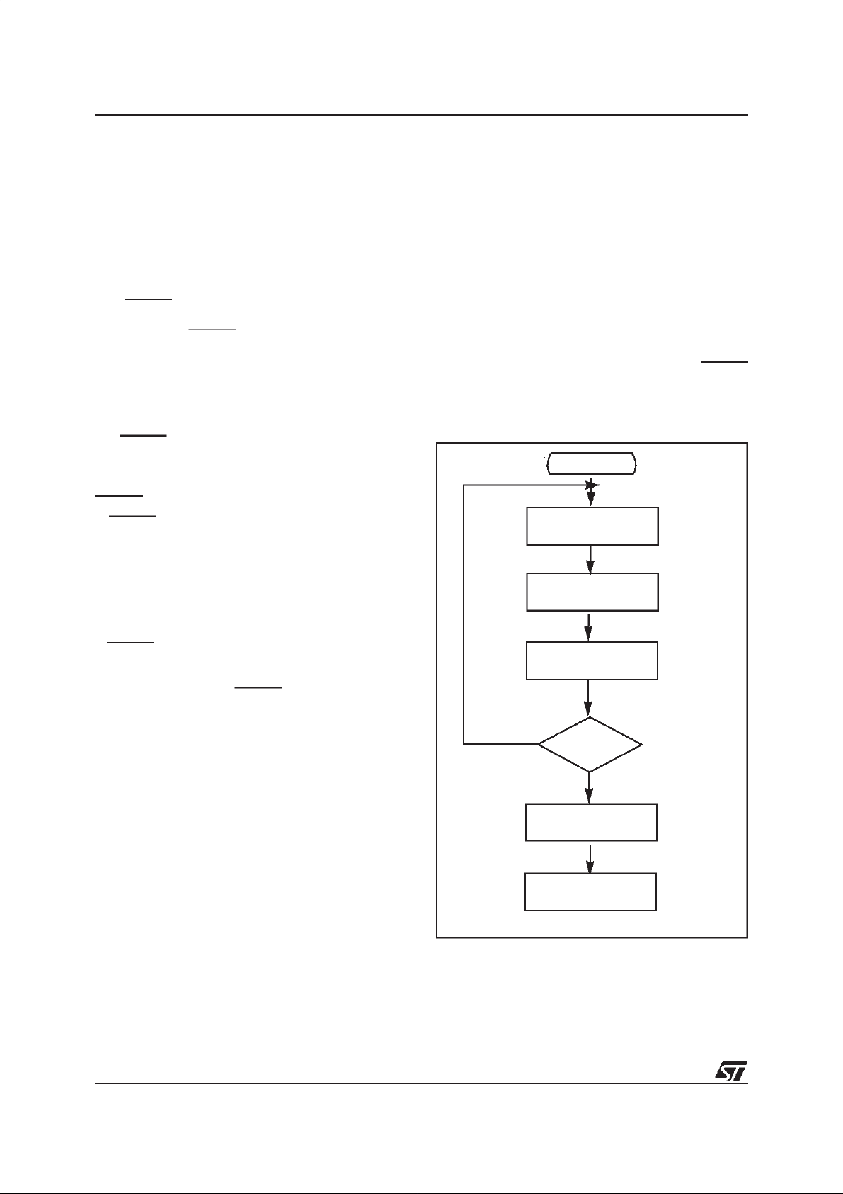
Figure 13. Reset and Interrupt Processing
RESET
NMI MASKSET
INT LATCH CLEARED
( IFPRESENT )
SELECT
NMI MODE FLAGS
PUT FFEH
ON ADDRESSBUS
YES
IS RESETSTILL
PRESENT?
NO
LOAD PC
FROM RESETLOCATIONS
FFE/FFF
FETCH INSTRUCTION
VA000427
22/78
21
RESETS (Cont’d)
3.2.3 Watchdog Reset
The MCU provides a Watchdog timer function in
order to ensure graceful recovery from software
upsets. If the Watchdog register is not refreshed
before an end-of-count condition is reached, the
internal reset will be activated. This, amongst other things, resets the watchdog counter.
ues, allowing hysteresiseffect. Reference value in
case of voltage drop has been set lower than the
reference value for power-on in order to avoid any
parasitic Reset when MCU start’s running and
sinking current on the supply.
As long as the supply voltage is below the reference value, there is a internal and static RESET
command. The MCU can start only when the sup-
The MCU restarts just as though the Reset had
been generated by the RESET pin, including the
built-in stabilisation delay period.
3.2.4 LVD Reset
The on-chip Low Voltage Detector, selectable as
user option, features static Reset when supply
voltage is below a reference value. Thanks to this
feature, external reset circuit can be removed
while keeping the application safety. This SAFE
RESET is effective as well in Power-on phase as
ply voltage rises over the reference value. Therefore, only two operating mode exist for the MCU:
RESET active below the voltage reference, and
running mode over the voltage reference as
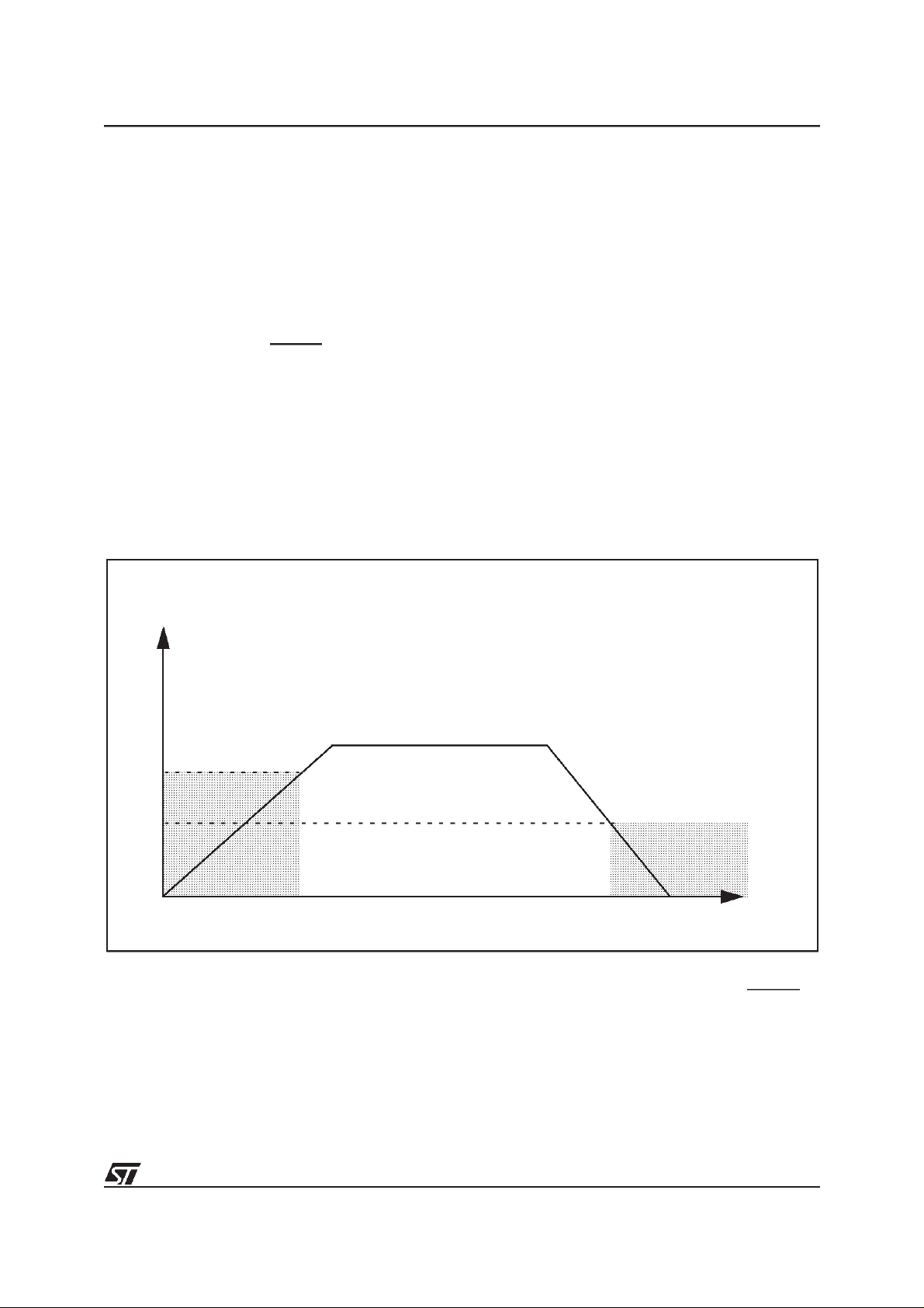
shown on the Figure 14., that represents a powerup, power-down sequence.
Note: When the RESET state is controlled by one
of the internal RESET sources (Low Voltage Detector, Watchdog, Power on Reset), the RESET
pin is tied to low logic level.
in power supply drop with different reference val-
Figure 14. LVD Reset on Power-on and Power-down (Brown-out)
ST62T52C ST62T62C/E62C
V
DD
V
Up
V
dn
RESET
3.2.5 Application Notes
No external resistor is required between VDDand
the Reset pin, thanks to the built-in pull-up device.
RESET
time
VR02106A
Direct external connection of the pin RESET to
VDDmust be avoided in order to ensure safe behaviour of the internal reset sources (AND.Wired
structure).
22
23/78
ST62T52C ST62T62C/E62C
RESETS (Cont’d)
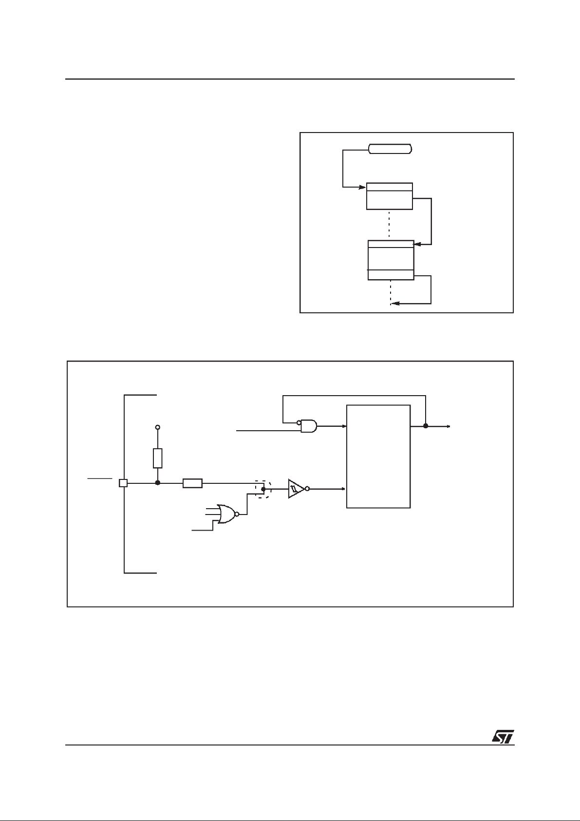
3.2.6 MCU Initialization Sequence
When a reset occurs the stack is reset, the PC is
loaded with the address of the Reset Vector (located in programROM starting at address 0FFEh). A
jump tothe beginning oftheuser programmustbe
coded at this address. Following a Reset, the Interrupt flag is automatically set, so that the CPU is
in NonMaskable Interrupt mode; this prevents the
initialisation routinefrom being interrupted. The initialisation routine should therefore be terminated
by a RETI instruction, in order to revert to normal
mode and enable interrupts. If nopendinginterrupt
is present at the endof theinitialisationroutine,the
MCU will continue by processing the instruction
immediately following the RETIinstruction.If,however, a pending interrupt is present, it will be serviced.
Figure 16. Reset Block Diagram
Figure 15. Reset and Interrupt Processing
RESET
JP:2 BYTES/4 CYCLES
RESET
VECTOR
INITIALIZATION
ROUTINE
JP
RETI: 1 BYTE/2 CYCLES
RETI
VA00181
V
DD
R
PU
R
RESET
POWER
WATCHDOGRESET
LVD RESET
1) Resistive ESD protection. Value not guaranteed.
ESD
ON RESET
f
OSC
1)
AND. Wired
RESET
CK
COUNTER
RESET
ST6
INTERNAL
RESET
VR02107A
24/78
23
 Loading...