

SGS Thomson Microelectronics ST62T01B6-SWD, ST62T01B6-HWD Datasheet
Rev. 3.0
June 2000 1/104
ST6200C/ST6201C/ST6203C
8-BIT MCUs WITH A/D CONVERTER,
TWO TIMERS, OSCILLATOR SAFEGUARD & SAFE RESET
■ Memories
– 1K or 2K bytes Program memory (OTP,
EPROM, FASTROM or ROM) with read-out
protection
– 64 bytes RAM
■ Clock, Reset and Supply Management
– Enhanced reset system
– Low Voltage Detector (LVD) for Safe Reset
– Clock sources: crystal/ceramic resonator or
RC network, external clock, backup oscillator
(LFAO)
– Oscillator Safeguard (OSG)
– 2 Power SavingModes: Wait and Stop
■ Interrupt Management
– 4 interrupt vectors plus NMI and RESET
– 9 external interruptlines (on 2 vectors)
■ 9 I/O Ports
– 9 multifunctional bidirectional I/O lines
– 4 alternate function lines
– 3 high sink outputs (20mA)
■ 2 Timers
– Configurable watchdog timer
– 8-bit timer/counter with a 7-bit prescaler
■ 1 Analog peripheral
– 8-bit ADC with 4 input channels (except on
ST6203C)
■ Instruction Set
– 8-bit data manipulation
– 40 basic instructions
– 9 addressing modes
– Bit manipulation
■ Development Tools
– Full hardware/software development package
Device Summary
(See Section 12.5 for Ordering Information)
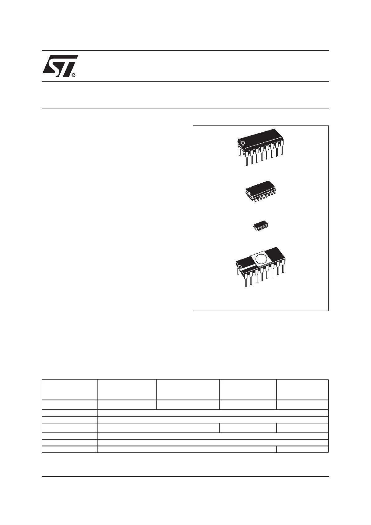
PDIP16
SO16
CDIP16W
SSOP16
Features
ST62T00C(OTP)
ST6200C(ROM)
ST62P00C(FASTROM)
ST62T01C(OTP)
ST6201C(ROM)
ST62P01C(FASTROM)
ST62T03C(OTP)
ST6203C(ROM)
ST62P03C(FASTROM)
ST62E01C(EPROM)
Program memory - bytes 1K 2K 1K 2K
RAM - bytes 64
Operating Supply 3.0V to 6V
Analog Inputs 4 - 4
Clock Frequency 8MHz Max
Operating Temperature -40°C to +125°C
Packages PDIP16 / SO16 / SSOP16 CDIP16W
1

Table of Contents
104
2/104
2
1 INTRODUCTION . . . . . . . . . . . . . . . . . . . . . .........................................6
2 PIN DESCRIPTION . . . . . . . . . . . . ................................................ 7
3 MEMORY MAPS, PROGRAMMING MODES AND OPTION BYTES . . . . . . . . . . . . . . . . . . . . . . 8
3.1 MEMORY AND REGISTER MAPS . ......................................... 8
3.1.1 Introduction . . . ..................................................... 8
3.1.2 Program Space . . . . . . . . . . . . . . . . . . . . ................................10
3.1.3 Readout Protection . . . . . . ...........................................10
3.1.4 Data Space . . . . . . . . . . . . . . . . . . . . . . . . . .............................. 10
3.1.5 Stack Space . . . . . . . . . . . . ........................................... 10
3.1.6 Data ROM Window . . ............................................... 12
3.2 PROGRAMMING MODES . ............................................... 14
3.2.1 Program Memory . . . ................................................ 14
3.2.2 EPROM Erasing .................................................... 14
3.3 OPTION BYTES . . . ....................................................15
4 CENTRAL PROCESSING UNIT . . ............................................... 16
4.1 INTRODUCTION . ...................................................... 16
4.2 MAIN FEATURES . . . . . . . . . . . . . . . . . . . . . . . . . . . . . . . . . . .................... 16
4.3 CPU REGISTERS . . . . . . . . . . . . . . . . . . . . . ................................. 16
5 CLOCKS, SUPPLY AND RESET . . . . . . . . . . . . . . . . . . . . . . . . . . . . . . . . . . . . . . . . . . . . . . . . 18
5.1 CLOCK SYSTEM . ...................................................... 18
5.1.1 Main Oscillator . .. . . . . . . . . . . . . . . . . . ................................. 19
5.1.2 Oscillator Safeguard (OSG) . . . ........................................ 20
5.1.3 Low Frequency Auxiliary Oscillator (LFAO) . . . . . . . . . . . .. . . . . . . . . . . . . . . . . . . 21
5.1.4 Register Description . . . . . . ........................................... 21
5.2 LOW VOLTAGE DETECTOR (LVD) . . . . . . . . ................................22
5.3 RESET . . . . . . . . . . . . . . . . . . . . . . . ........................................ 23
5.3.1 Introduction . . . .................................................... 23
5.3.2 RESET sequence . . . ............................................... 23
5.3.3 RESET Pin . . . . . . . . . ............................................... 24
5.3.4 Watchdog Reset . . . . . . . . . . . . . . . . . . ................................. 25
5.3.5 LVD Reset . . . . . . . . . ...............................................25
6 INTERRUPTS . . ............................................................. 26
6.1 INTERRUPT RULES AND PRIORITY MANAGEMENT . . . . . . . . . . . . . . . . . . . . . . . . . 27
6.2 INTERRUPTS AND LOW POWER MODES . . . . . . . . . . . . . . . . . . . . . . . . . . . . . . . . . . 27
6.3 NON MASKABLE INTERRUPT . . . . . . . . . . ..................................27
6.4 PERIPHERAL INTERRUPTS . . ...........................................27
6.5 EXTERNAL INTERRUPTS (I/O PORTS) . . . .................................28
6.5.1 Notes on using External Interrupts .. . . . . . . .............................. 28
6.6 INTERRUPT HANDLING PROCEDURE . . . . . . . . . . . . . . . . . . . . . . . . . . . . . ........ 29
6.6.1 Interrupt Response Time . . . . . . . . . . . .................................. 29
6.7 REGISTER DESCRIPTION . . . . . . . . . . . . . . . . . . . . . . . . . . . . . . . . . . . . . . . ........ 30

Table of Contents
3/104
3
7 POWER SAVING MODES . . . . . . . . . . ...........................................31
7.1 INTRODUCTION . ...................................................... 31
7.2 WAIT MODE . . . . . . . . . . . ............................................... 32
7.3 STOP MODE . . . . . . .................................................... 33
7.4 NOTES RELATED TO WAIT AND STOP MODES .............................35
7.4.1 Exit from Wait and Stop Modes . . . . ....................................35
7.4.2 Recommended MCU Configuration . . . . . . . . . . . . . . . . . . . . . . . . . . . . . ........ 35
8 I/O PORTS . . . . . . . . . . . . . . . . . . . . . . . . . . ........................................ 36
8.1 INTRODUCTION . ...................................................... 36
8.2 FUNCTIONAL DESCRIPTION . . . . ........................................36
8.2.1 Digital input modes . . . . . . ...........................................36
8.2.2 Analog inputs . . . . . . . ...............................................36
8.2.3 Output modes . . . . . . ............................................... 36
8.2.4 Alternate functions . . . ...............................................36
8.2.5 Instructions NOT to be used to access Port Data registers (SET, RES, INC and DEC) 38
8.2.6 Recommendations . . . . . . . ...........................................38
8.3 LOW POWER MODES . . . . . . . . . . ........................................38
8.4 INTERRUPTS . . . . . . . . . . . . . . . . . . . . . . . . ................................. 38
8.5 REGISTER DESCRIPTION . . . . . . . . . . . . . . . . . . . . . . . . . . . . . . . . . . . . . . . ........ 40
9 ON-CHIP PERIPHERALS . . . . . . . . . . . ........................................... 41
9.1 WATCHDOG TIMER (WDG) . . . . . . . . . . . . . . . . . . . ........................... 41
9.1.1 Introduction . . . .................................................... 41
9.1.2 Main Features . . . . . . ...............................................41
9.1.3 Functional Description . . . . ...........................................42
9.1.4 Recommendations . . . . . . . ...........................................42
9.1.5 Low Power Modes . . . ............................................... 43
9.1.6 Interrupts . . . . . . . . . . . . . . . . . . . . . . . . ................................. 43
9.1.7 Register Description . . . . . . ........................................... 44
9.2 8-BIT TIMER . . . . ...................................................... 45
9.2.1 Introduction . . . .................................................... 45
9.2.2 Main Features . . . . . . ...............................................45
9.2.3 Counter/Prescaler Description . . . . . . . . . . . . . . . . . . . . . . . . . . . . . . . . . ........ 46
9.2.4 Functional Description . . . . ...........................................47
9.2.5 Low Power Modes . . . ............................................... 49
9.2.6 Interrupts . . . . . .................................................... 49
9.2.7 Register Description . . . . . . ........................................... 50
9.3 A/D CONVERTER (ADC) . . . . . . . . . . . . . . . . . . . . . ........................... 51
9.3.1 Introduction . . . .................................................... 51
9.3.2 Main Features . . . . . . ...............................................51
9.3.3 Functional description . . . . . . . . . . . . . . . . . . . . ........................... 52
9.3.4 Recommendations . . . . . . . ...........................................53
9.3.5 Low power modes . . . . . . . . . . . . . . . . . . ................................54
9.3.6 Interrupts . . . . . . . . . . . . . . . . . . . . . . . . ................................. 54
9.3.7 Register description . . . . . . ...........................................54

Table of Contents
104
4/104
10 INSTRUCTION SET . . . . . . . . . . . . . . . . . . . . . . . . ................................. 55
10.1 ST6 ARCHITECTURE . . . . . . . . . . . . . . . . . .................................. 55
10.2 ADDRESSING MODES . . . . . . . . . . . . . . . . . . ................................55
10.3 INSTRUCTION SET . . . . . . . . . . . . . . . . . . . ................................. 56
11 ELECTRICAL CHARACTERISTICS . . . . ......................................... 61
11.1 PARAMETER CONDITIONS . . . . . . . . . . . . . . . . .............................. 61
11.1.1Minimum and Maximum values ........................................61
11.1.2Typical values . . . . . . . . . . ...........................................61
11.1.3Typical curves . . . . . . . . . . . . . ........................................ 61
11.1.4Loading capacitor . . . . . . . . . . . . . . . . . .................................. 61
11.1.5Pin input voltage . . . . . . . . . . . . . . . . . . . . . . . . . . . . . . . . . . . . . . . . . . . . . . . . . . . 61
11.2 ABSOLUTE MAXIMUM RATINGS . . . . . . . . . . . . . . . . . . . . . . . . . . . . . . . . . . . . . . . . . 62
11.2.1Voltage Characteristics . . . . . . . . . . . . . . . . . . . . . . . . . . . . . . . . . . . . . . . . . . . . . . 62
11.2.2Current Characteristics . . . . . . . . . . . . . . . . .............................. 62
11.2.3Thermal Characteristics . . . . . . . . . .................................... 62
11.3 OPERATING CONDITIONS . . . . . . . . . . .................................... 63
11.3.1General Operating Conditions . . . . .................................... 63
11.3.2Operating Conditions with Low Voltage Detector (LVD) . .................... 64
11.4 SUPPLY CURRENT CHARACTERISTICS . . . ................................65
11.4.1RUN Modes . . . . . . . . . . . . . . . . . . . . . . . . . . . . . . . . . . .................... 65
11.4.2WAIT Modes . . . . . . . . . . . ........................................... 66
11.4.3STOP Mode . . . ................................................... 69
11.4.4Supply and Clock System . . . . . . . . . . . . . . . . . . . . . . . . . . . . . . . . . . . . . . . . . . . . 70
11.4.5On-Chip Peripherals . . . . . ...........................................70
11.5 CLOCK AND TIMING CHARACTERISTICS . . . . . . . . . . . . . . . . . . . . . . . ...........71
11.5.1General Timings . . . . . . . . . . . . . . . . . . . . . . . . . . . . . . . . . . . . . . . . . . . . . . . . . . . 71
11.5.2External Clock Source . . . . . . . . . . . ....................................71
11.5.3Crystal and Ceramic Resonator Oscillators . . . . ........................... 72
11.5.4RC Oscillator . . .................................................... 73
11.5.5Oscillator Safeguard (OSG) and Low Frequency Auxiliary Oscillator (LFAO) . . . . . 74
11.6 MEMORY CHARACTERISTICS . . . ........................................75
11.6.1RAM and Hardware Registers . . . . . . . . . . . . . . . . . . . . . . . . . ............... 75
11.6.2EPROM Program Memory . . . . . . . . . . ................................. 75
11.7 EMC CHARACTERISTICS . . . . . . . . . . . . . . . . . . . . . . . . . . . . . . . . . . . . . . . . . . . . . . . 76
11.7.1Functional EMS . . . . . ............................................... 76
11.7.2Absolute Electrical Sensitivity . . . . . . . . . . . . . . ........................... 77
11.7.3ESD Pin Protection Strategy . . . . . . . . . . . . . . . . . . . . . . . . . . . . . . . . . . . . . . . . . . 79
11.8 I/O PORT PIN CHARACTERISTICS ........................................80
11.8.1General Characteristics . . . . . . . . . . . . ..................................80
11.8.2Output Driving Current . . . . ........................................... 81
11.9 CONTROL PIN CHARACTERISTICS . . . . . .................................. 84
11.9.1Asynchronous RESET Pin . . . . . . . . . . . . . . . . . ........................... 84
11.9.2NMI Pin . . . . . . . . . . . . . . . ...........................................85
1

Table of Contents
5/104
11.10 TIMER PERIPHERAL CHARACTERISTICS . . . . . . . . . . . . . . . . . . . . . . . . . . ........86
11.10.1Watchdog Timer .. . . . . . . . . . . . . . . . . . . . . . . . . . . . . . . . . . . . . . . . . ........ 86
11.10.28-Bit Timer . . . . . . . . . . . . ...........................................86
11.11 8-BIT ADC CHARACTERISTICS .. . . . . . . .................................. 87
12 GENERAL INFORMATION .................................................... 89
12.1 PACKAGE MECHANICAL DATA . . . . . . . . . . . . .............................. 89
12.2 THERMAL CHARACTERISTICS . . . . . . . . . . . . . . . . . . . . . . .................... 91
12.3 SOLDERING AND GLUEABILITY INFORMATION . . . . . . . . . . . . . . . . . . . . . ........92
12.4 PACKAGE/SOCKET FOOTPRINT PROPOSAL . . . . . . . . . . . .................... 93
12.5 ORDERING INFORMATION . . . . . . . . .. . . . . . . .............................. 94
12.6 TRANSFER OF CUSTOMER CODE . . . . . . . . . . . . . . . . . . . . . . . . . . . . . . . ........95
12.6.1FASTROM version . . . ............................................... 95
12.6.2ROM VERSION .................................................... 97
13 DEVELOPMENT TOOLS . . . . . . . . . . ........................................... 99
14 ST6 APPLICATION NOTES . . . . . . . . . . . . . . . . . . . . . ............................. 101
15 SUMMARY OF CHANGES . .................................................. 103
16 TO GET MORE INFORMATION . .............................................. 103
1
ST6200C/ST6201C/ST6203C
6/104
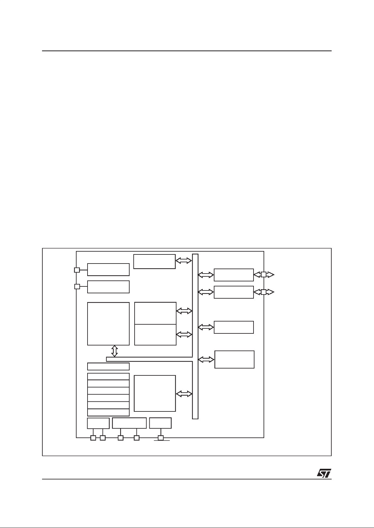
1 INTRODUCTION
The ST6200C, 01C and 03C devices are low cost
members of theST62xx 8-bit HCMOS family of microcontrollers, which is targeted at low to medium
complexity applications. All ST62xx devices are
based on a building block approach: a common
core is surrounded by a number of on-chip peripherals.
The ST62E01C isthe erasable EPROM versionof
the ST62T00C,T01 and T03Cdevices, which may
be used during the development phase for the
ST62T00C, T01 and T03C target devices, as well
as the respective ST6200C, 01C and 03C ROM
devices.
OTP and EPROM devices are functionally identical. OTP devices offer all the advantages of user
programmability at low cost, which make them the
ideal choice in a wide range of applications where
frequent code changes, multiple code versions or
last minute programmability are required.
The ROM based versions offer the same functionality, selecting the options defined in the program-
mable option bytes of the OTP/EPROM versions
in the ROM option list (See Section 12.6 on page
95).
The ST62P00C, P01C and P03C are the Factory
Advanced Service Technique ROM (FASTROM)
versions of ST62T00C, T01 and T03COTP devices.
They offer the same functionality as OTP devices,
but they do not have to be programmed by the
customer (See Section 12 on page 89).
These compact low-cost devices feature a Timer
comprising an 8-bit counter with a 7-bit programmable prescaler, an 8-bit A/D Converter with 4 analog inputs (depending on device, see device
summary on page 1) and a Digital Watchdog timer, making them well suited for a wide range of automotive, appliance and industrial applications.
For easy reference, all parametric dataare located
in Section 11 on page 61.
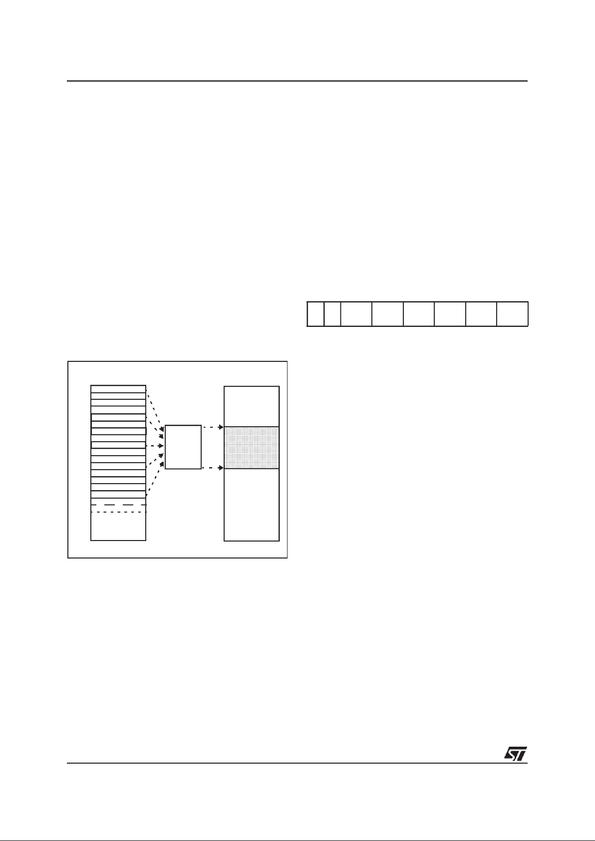
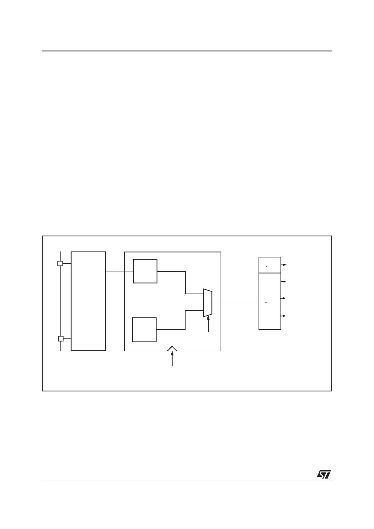
Figure 1. Block Diagram
TEST
NMI INTERRUPTS
PROGRAM
PC
STACKLEVEL 1
STACKLEVEL 2
STACKLEVEL 3
STACKLEVEL 4
STACKLEVEL 5
STACKLEVEL 6
POWER
SUPPLY
OSCILLATOR
RESET
DATA ROM
USER
SELECTABLE
DATA RAM
64 Bytes
PORT A
PORT B
TIMER
8-BIT CORE
TEST/V
PP
8-BIT *
A/D CONVERTER
PA1..PA3 (20mA Sink)
PB0..PB1
V
DDVSS
OSCin OSCout RESET
WATCHDOG
:
MEMORY
TIMER
(1K or 2K Bytes)
PB3, PB5..PB7 / Ain*
* Depending on device. See device summary on page 1.
4
ST6200C/ST6201C/ST6203C
7/104
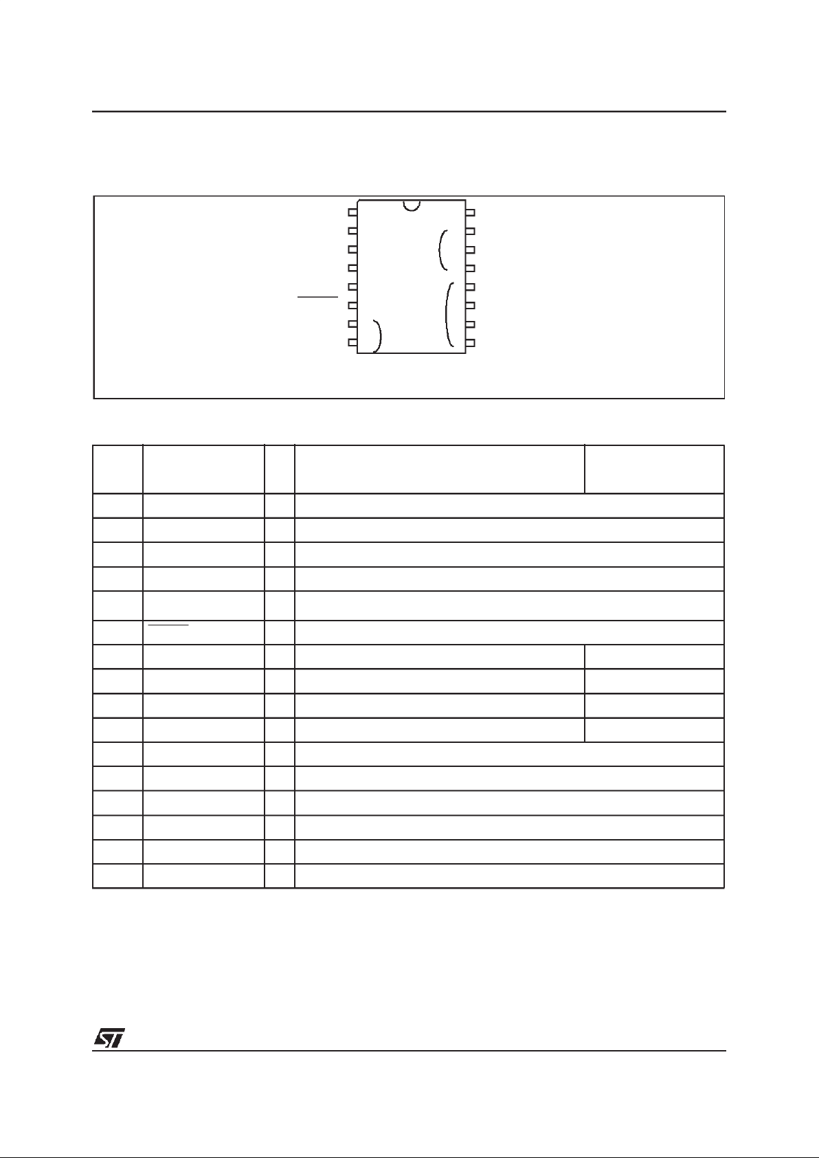
2 PIN DESCRIPTION
Figure 2. 16-Pin Package Pinout
Table 1. Device Pin Description
Legend / Abbreviations for Table 1:
* Depending on device. See device summary on page 1.
I = input, O = output, S = supply, IPU = input pull-up
The input with pull-up configuration (reset state) is valid as long as the user software does not change it.
Refer to Section 8 ”I/O PORTS” onpage 36 for more detailson the software configuration of the I/O ports.
16
15
14
13
12
11
10
9
1
2
3
4
5
6
7
8
V
DD
PB5/Ain*
Ain*/PB6
Ain*/PB7
RESET
V
PP
/TEST
NMI
OSCout
OSCin
V
SS
PB3/Ain*
PB1
PB0
PA3/20mA Sink
PA2/20mA Sink
PA1/20mA Sink
it2
it1
itX associated interrupt vector
* Depending on device. See device summary on page1.
it2
Pin n° Pin Name
Type
Main Function
(after Reset)
Alternate Function
1V
DD
S Main power supply
2 OSCin I External clock input or resonator oscillator inverter input
3 OSCout O Resonator oscillator inverter output or resistor input for RC oscillator
4 NMI I Non maskable interrupt (falling edge sensitive)
5V
PP
/TEST
Must be held at Vss for normal operation, if a 12.5V level is applied to the pin
during the reset phase, the device enters EPROM programming mode.
6 RESET I/O Top priority non maskable interrupt (active low)
7 PB7/Ain* I/O Pin B7 (IPU) Analog input
8 PB6/Ain* I/O Pin B6 (IPU) Analog input
9 PB5/Ain* I/O Pin B5 (IPU) Analog input
10 PB3/Ain* I/O Pin B3 (IPU) Analog input
11 PB1 I/O Pin B1 (IPU)
12 PB0 I/O Pin B0 (IPU)
13 PA3/ 20mA Sink I/O Pin A3 (IPU)
14 PA2/ 20mA Sink I/O Pin A2 (IPU)
15 PA1/ 20mA Sink I/O Pin A1 (IPU)
16 V
SS
S Ground
ST6200C/ST6201C/ST6203C
8/104
3 MEMORY MAPS, PROGRAMMING MODES AND OPTION BYTES
3.1 MEMORY AND REGISTER MAPS
3.1.1 Introduction
The MCU operates in three separate memory
spaces: Program space, Data space, and Stack
space. Operation in thesethree memory spaces is
described in the following paragraphs.
Briefly, Program space contains user program
code in OTP and user vectors; Data space contains user data in RAM and in OTP, and Stack
space accommodates six levels of stack for subroutine and interrupt service routine nesting.
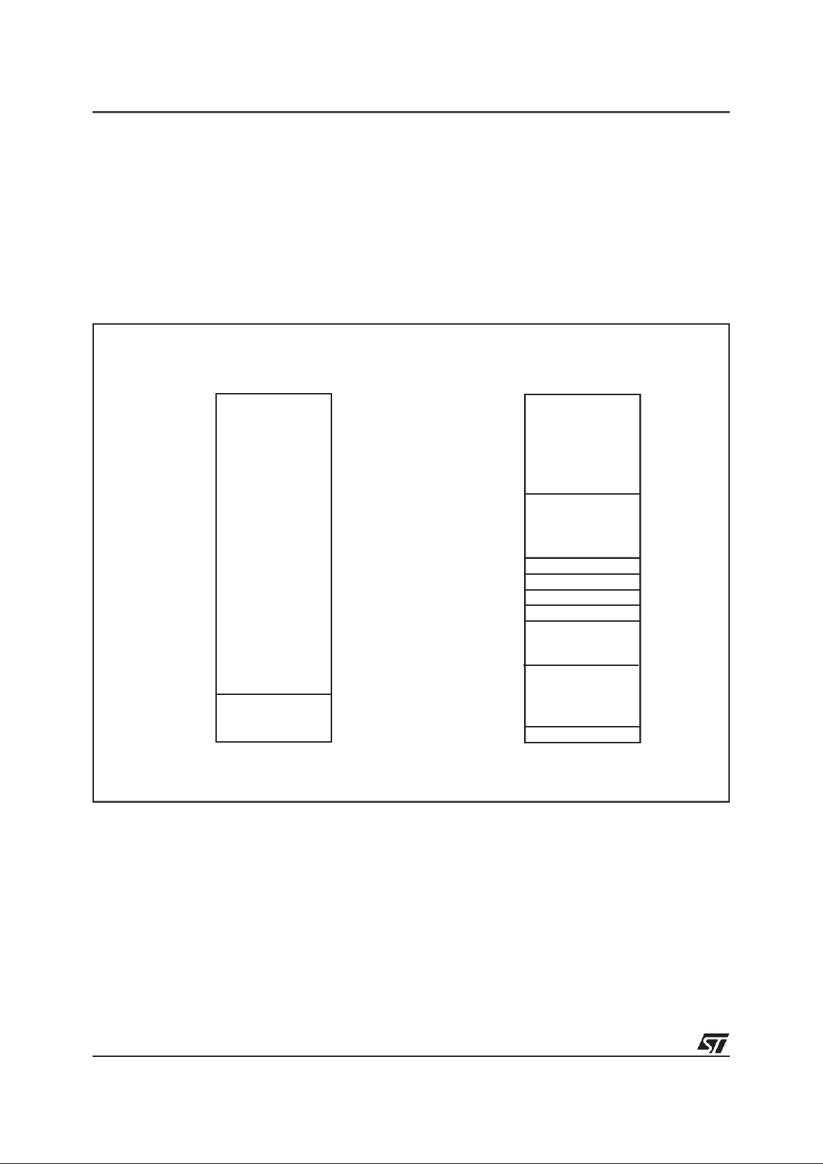
Figure 3. Memory Addressing Diagram
PROGRAM SPACE
PROGRAM
INTERRUPT &
RESET VECTORS
ACCUMULATOR
RAM
X REGISTER
Y REGISTER
V REGISTER
W REGISTER
000h
03Fh
040h
07Fh
080h
081h
082h
083h
084h
0C0h
0FFh
DATA SPACE
000h
0FF0h
0FFFh
MEMORY
WINDOW
DATA ROM
RESERVED
HARDWARE
CONTROL
REGISTERS
0BFh
(see Table 2)
(see Figure 4)
1

ST6200C/ST6201C/ST6203C
9/104
MEMORY MAP (Cont’d)
Figure 4. Program Memory Map
RESERVED
*
0000h
07FFh
0800h
087Fh
NOT IMPLEMENTED
RESERVED
*
USER
PROGRAM MEMORY
1024 BYTES
0880h
0F9Fh
0FA0h
0FEFh
0FF0h
0FF7h
0FF8h
0FFBh
0FFCh
0FFDh
0FFEh
0FFFh
RESERVED
*
INTERRUPT VECTORS
NMI VECTOR
USER RESET VECTOR
(*) Reserved areas should be filled with 0FFh
ST6200C, ST6203C
0000h
07FFh
0800h
087Fh
NOT IMPLEMENTED
RESERVED
*
USER
PROGRAM MEMORY
1824 BYTES
0880h
0F9Fh
0FA0h
0FEFh
0FF0h
0FF7h
0FF8h
0FFBh
0FFCh
0FFDh
0FFEh
0FFFh
RESERVED
*
RESERVED
*
INTERRUPT VECTORS
NMI VECTOR
USER RESET VECTOR
ST6201C
1

ST6200C/ST6201C/ST6203C
10/104
MEMORY MAP (Cont’d)
3.1.2 Program Space
Program Space comprises the instructions to be
executed, the data required for immediate addressing mode instructions, the reserved factory
test area and the user vectors. Program Space is
addressed via the 12-bit ProgramCounter register
(PC register). Thus, the MCU is capable of addressing 4K bytes of memory directly.
3.1.3 Readout Protection
The Program Memory in in OTP, EPROM or ROM
devices can be protected against external readout
of memory by setting the Readout Protectionbit in
the option byte (Section 3.3 on page 15).
In the EPROM parts, Readout Protection option
can be desactivated only by U.V. erasure that also
results in the whole EPROM context being erased.
Note: Once the Readout Protection is activated, it
is no longer possible, even for STMicroelectronics,
to gain access to the OTP or ROM contents. Returned parts can therefore not be accepted if the
Readout Protection bit is set.
3.1.4 Data Space
Data Space accommodates all the data necessary
for processing the user program. This space comprises the RAM resource, the processor core and
peripheral registers, as well as read-only data
such as constants and look-up tables in OTP/
EPROM.
3.1.4.1 Data ROM
All read-only data is physically stored in program
memory, which also accommodates the Program
Space. The program memory consequently contains the program code to be executed, as well as
the constants and look-up tables required by the
application.
The Data Space locations in which the different
constants and look-up tables are addressed bythe
processor core may be thought of as a 64-byte
window through which it is possible to access the
read-only data stored in OTP/EPROM.
3.1.4.2 Data RAM
The data space includes the user RAM area, the
accumulator (A), the indirect registers (X), (Y), the
short direct registers (V), (W), the I/O port registers, the peripheral data and control registers, the
interrupt option register and the Data ROM Window register (DRWR register).
3.1.5 Stack Space
Stack space consists of six 12-bit registers which
are used to stack subroutine and interrupt return
addresses, as well as the current program counter
contents.
1

ST6200C/ST6201C/ST6203C
11/104
MEMORY MAP (Cont’d)
Table 2. Hardware Register Map
Legend:
x = undefined, R/W = Read/Write, Ro = Read-only Bit(s) in the register, Wo = Write-only Bit(s)
in the register.
Notes:
1. The contents of the I/O port DR registers are readable only in output configuration. In input configuration, the values of the I/O pins are returned instead of the DR register contents.
2. The bits associated with unavailable pins mustalways be kept at their reset value.
3. Do notuse single-bit instructions (SET, RES...) on Port Data Registersif anypin ofthe port is configured
in input mode (refer to Section 8 ”I/O PORTS” on page 36 for more details).
4. Depending on device. See device summary on page 1.
Address Block
Register
Label
Register Name
Reset
Status
Remarks
080h
to 083h
CPU X,Y,V,W
X,Y index registers
V,W short direct registers
xxh R/W
0C0h
0C1h
I/O Ports
DRA
1) 2) 3)
DRB
1) 2) 3)
Port A Data Register
Port B Data Register
00h
00h
R/W
R/W
0C2h
0C3h
Reserved (2 Bytes)
0C4h
0C5h
I/O Ports
DDRA
2)
DDRB
2)
Port A Direction Register
Port B Direction Register
00h
00h
R/W
R/W
0C6h
0C7h
Reserved (2 Bytes)
0C8h IOR Interrupt Option Register xxh Write-only
0C9h DRWR Data ROM Window register xxh Write-only
0CAh
0CBh
Reserved (2 Bytes)
0CCh
0CDh
I/O Ports
ORA
2)
ORB
2)
Port A Option Register
Port B Option Register
00h
00h
R/W
R/W
0CEh
0CFh
Reserved (2 bytes)
0D0h
0D1h
ADC
ADR
ADCR
A/D Converter Data Register
A/D Converter Control Register
xxh
40h
Read-only
Ro/Wo
0D2h
0D3h
0D4h
Timer 1
PSCR
TCR
TSCR
Timer 1 Prescaler Register
Timer 1 Downcounter Register
Timer 1 Status Control Register
7Fh
0FFh
00h
R/W
R/W
R/W
0D5h
to 0D7h
Reserved (3 Bytes)
0D8h
Watchdog
Timer
WDGR Watchdog Register 0FEh R/W
0D9h
to 0FEh
Reserved (38 Bytes)
0FF CPU A Accumulator xxh R/W
1
ST6200C/ST6201C/ST6203C
12/104
MEMORY MAP (Cont’d)
3.1.6 Data ROM Window
The Data read-only memory window is located
from address 0040h to address 007Fh in Data
space. It allows direct reading of 64 consecutive
bytes located anywhere in program memory, between address 0000h and 0FFFh.
There are 64 blocks of 64 bytes in a 4K device:
– Block 0is related to the address range 0000h to
003Fh.
– Block 1is related to the address range 0040h to
007Fh.
and so on...
All the program memory can therefore be used to
store either instructions or read-only data. The
Data ROM window can be moved in steps of 64
bytes along the program memory by writing the
appropriate code inthe Data ROM WindowRegister (DRWR).
Figure 5. Data ROM Window
3.1.6.1 Data ROM Window Register (DRWR)
The DRWR can be addressed like any RAM location in the Data Space.
This register is used to select the 64-byte block of
program memory to be read in the Data ROM window (from address 40h to address 7Fh in Data
space). The DRWR register is not cleared on reset, therefore it must be written to before accessing the Data read-only memory window area for
the first time.
Address: 0C9h — Write Only
Reset Value = xxh (undefined)
Bits 6, 7 = Not used.
Bit 5:0 = DRWR[5:0]
Data read-only memory Win-
dow Register Bits.
These are the Data read-only
memory Window bits that correspondto the upper
bits of the data read-only memory space.
Caution:
This register is undefined on reset, it is
write-only, thereforedo notread it nor access it using single-bit instructions (SET, RES...).
0000h
0FFFh
000h
040h
07Fh
0FFh
DATA ROM
WINDOW
DATA SPACE
64-BYTE
ROM
PROGRAM
SPACE
70
- - DRWR5 DRWR4 DRWR3 DRWR2 DRWR1 DRWR0
1
ST6200C/ST6201C/ST6203C
13/104
MEMORY MAP (Cont’d)
3.1.6.2 Data ROM Window memory addressing
In cases where some data (look-up tables for example) are stored in program memory, reading
these data requires the use of the Data ROM window mechanism. To do this:
1. The DRWR register has to be loaded with the
64-byte block number where the data are located
(in program memory). This number also gives the
start address of the block.
2. Then, the offset address of the byte in the Data
ROM Window (corresponding to the offset in the
64-byte block in programmemory) has to be loaded in a register (A, X,...).
When the above two steps are completed, the
data can be read.
To understand how to determine the DRWR and
the content of the register, please refer to the example shown in Figure 6. In any case the calcula-
tion is automatically handled by the ST6 development tools.
Please refer to the user manual of the correspoding tool.
3.1.6.3 Recommendations
Care is required when handling the DRWR register as it is write only. For this reason, the DRWR
contents should not be changed while executing
an interrupt service routine, as the service routine
cannot save and then restore the register’s previous contents. If it is impossible to avoid writing to
the DRWR during the interrupt service routine, an
image of the register must be saved in a RAM location, and each time the program writes to the
DRWR, it must also write to the image register.
The image register must be written first so that, if
an interrupt occurs between the two instructions,
the DRWR is not affected.
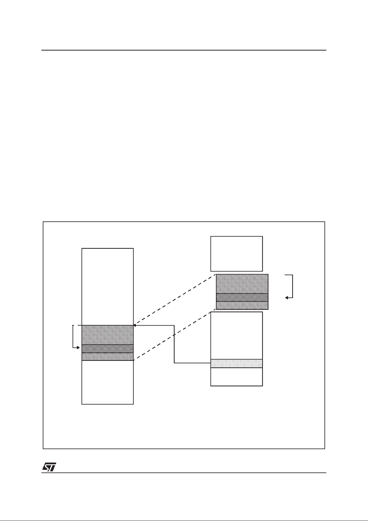
Figure 6. Data ROM Window Memory Addressing
DATA
PROGRAM SPACE
DATA SPACE
0000h
0400h
0421h
07FFh
64 bytes
OFFSET
000h
040h
061h
07Fh
OFFSET
21h
0FFh
DRWR
DATA address in Program memory : 421h
DRWR content : 421h / 3Fh (64) = 10H data is located in 64-bytes window number 10h
64-byte window start address : 10h x 3Fh = 400h
Register (A, X,...)content : Offset = (421h - 400h) + 40h ( Data ROM Window start address in data space) = 61h
10h
DATA
1

ST6200C/ST6201C/ST6203C
14/104
3.2 PROGRAMMING MODES
3.2.1 Program Memory
Table3.EPROM/OTP programmingmodeissetby
a +12.5Vvoltageapplied totheTEST/VPPpin.The
programmingflowofthe ST62T00C,T01/E01Cand
T03C is described in the User Manual of the
EPROM Programming Board.
Table 4. ST6200C/03C Program Memory Map
Table 5. ST6201C Program Memory Map
Note: OTP/EPROM devices can be programmed
with the development tools available from
STMicroelectronics (please refer to Section 13 on
page 99).
3.2.2 EPROM Erasing
The EPROM devices can be erased by exposure
to Ultra Violet light. The characteristics of the MCU
are such that erasure begins when the memory is
exposed to light with a wave lengths shorter than
approximately 4000Å. It should be noted that sunlight and some types of fluorescent lamps have
wavelengths in the range 3000-4000Å.
It is thus recommended that the window of the
MCU packages be covered by an opaque label to
prevent unintentional erasure problems when testing the application in such an environment.
The recommended erasure procedure is exposure
to short wave ultraviolet light which have a wavelength 2537Å. The integrated dose (i.e. U.V. intensity x exposure time) for erasure should be a minimum of 30W-sec/cm2. The erasure time with this
dosage is approximately30 to 40 minutes using an
ultraviolet lamp with 12000µW/cm2power rating.
The EPROM device should be placed within
2.5cm (1inch) of the lamp tubes during erasure.
Device Address Description
0000h-0B9Fh
0BA0h-0F9Fh
0FA0h-0FEFh
0FF0h-0FF7h
0FF8h-0FFBh
0FFCh-0FFDh
0FFEh-0FFFh
Reserved
User ROM
Reserved
Interrupt Vectors
Reserved
NMI Interrupt Vector
Reset Vector
Device Address Description
0000h-087Fh
0880h-0F9Fh
0FA0h-0FEFh
0FF0h-0FF7h
0FF8h-0FFBh
0FFCh-0FFDh
0FFEh-0FFFh
Reserved
User ROM
Reserved
Interrupt Vectors
Reserved
NMI Interrupt Vector
Reset Vector
1

ST6200C/ST6201C/ST6203C
15/104
3.3 OPTION BYTES
Each deviceis available for production in user programmable versions (OTP) as well as in factory
coded versions (ROM). OTP devices are shipped
to customers with a default content (00h), while
ROM factory coded parts contain the code supplied by the customer. This implies that OTP devices have to be configured by the customer using
the OptionBytes while the ROM devices are factory-configured.
The two option bytes allow the hardware configuration of the microcontroller to be selected.
The option bytes have no address in the memory
map and can be accessed only in programming
mode (for example using a standard ST6 programming tool).
In masked ROM devices, the option bytes are
fixed in hardware by the ROM code (see Section
12.6.2 ”ROM VERSION” on page 97).
The option bytes can be only programmed once. It
is not possible tochange theselected optionsafter
they have been programmed.
MSB OPTION BYTE
Bit 15:11 = Reserved, must be always cleared.
Bit 10 = Reserved, must be always set.
Bit 9 = EXTCNTL
External STOP MODE control.
0: EXTCNTL mode not available. STOP mode is
not available with the watchdog active.
1: EXTCNTL mode available. STOP mode is avail-
able with the watchdogactive by setting NMIpin
to one.
Bit 8 = LVD
Low Voltage Detector
on/off
.
This option bit enable or disable the Low Voltage
Detector (LVD) feature.
0: Low Voltage Detector disabled
1: Low Voltage Detector enabled.
LSB OPTION BYTE
Bit 7 = PROTECT
Readout Protection.
This option bit enables or disables external access
to the internal program memory.
0: Program memory not read-out protected
1: Program memory read-out protected
Bit 6 = OSC
Oscillator selection
.
This option bit selects the main oscillator type.
0: Quartz crystal, ceramic resonator or external
clock
1: RC network
Bit 5 = Reserved, must be always cleared.
Bit 4 = Reserved, must be always set.
Bit 3 = NMI PULL
NMI Pull-Up
on/off.
This option bitenables or disables the internalpullup on the NMI pin.
0: Pull-up disabled
1: Pull-up enabled
Bit 2 = Reserved, must be always set.
Bit 1 = WDACT
Hardware or software watchdog.
This option bit selects the watchdog type.
0: Software (watchdog to be enabled by software)
1: Hardware (watchdog always enabled)
Bit 0 = OSGEN
Oscillator Safeguard
on/off.
This option bit enables or disables the oscillator
Safeguard (OSG) feature.
0: Oscillator Safeguard disabled
1: Oscillator Safeguard enabled
MSB OPTION BYTE
15 8
LSB OPTION BYTE
70
Reserved
EXT
CTL
LVD
PRO-
TECT
OSC Res. Res.
NMI
PULL
Res.
WD
ACT
OSG
EN
Default
Value
XXXXXXXXXXXXX X X X
1
ST6200C/ST6201C/ST6203C
16/104
4 CENTRAL PROCESSING UNIT
4.1 INTRODUCTION
The CPU Coreof ST6devicesisindependent ofthe
I/O or Memory configuration. As such, it may be
thought of as an independent central processor
communicating with on-chip I/O, Memory and Peripherals via internal address, data, and control
buses.
4.2 MAIN FEATURES
■ 40 basic instructions
■ 9 main addressing modes
■ Two 8-bit index registers
■ Two 8-bit short direct registers
■ Low power modes
■ Maskable hardware interrupts
■ 6-level hardware stack
4.3 CPU REGISTERS
TheST6FamilyCPUcorefeaturessixregisters and
three pairs of flags available to the programmer.
These are described in the following paragraphs.
Accumulator (A). The accumulator is an 8-bit
general purpose register used in all arithmetic calculations, logical operations, and data manipula-
tions. The accumulator can be addressed in Data
Space as a RAM location at address FFh. Thus
the ST6 can manipulate the accumulator just like
any other register in Data Space.
Index Registers (X, Y). These two registers are
used in Indirect addressing mode as pointers to
memory locations in Data Space. They can also
be accessed in Direct, Short Direct, or Bit Direct
addressing modes. They are mapped in Data
Space at addresses 80h (X) and 81h (Y) and can
be accessed like any other memory location.
Short Direct Registers (V, W). These two registers are used in Short Direct addressing mode.
This means that the data stored in V or W can be
accessed with aone-byte instruction (four CPU cycles). V and W can also be accessed using Direct
and Bit Direct addressing modes. They are
mapped in Data Space at addresses 82h (V) and
83h (W) and canbe accessed like any other memory location.
Note: The X and Y registers can also be used as
Short Directregisters inthe same way as V and W.
Program Counter (PC). Theprogram counter is a
12-bit register which contains the address of the
next instruction to be executed by the core. This
ROM location may be an opcode, an operand, or
the address of an operand.
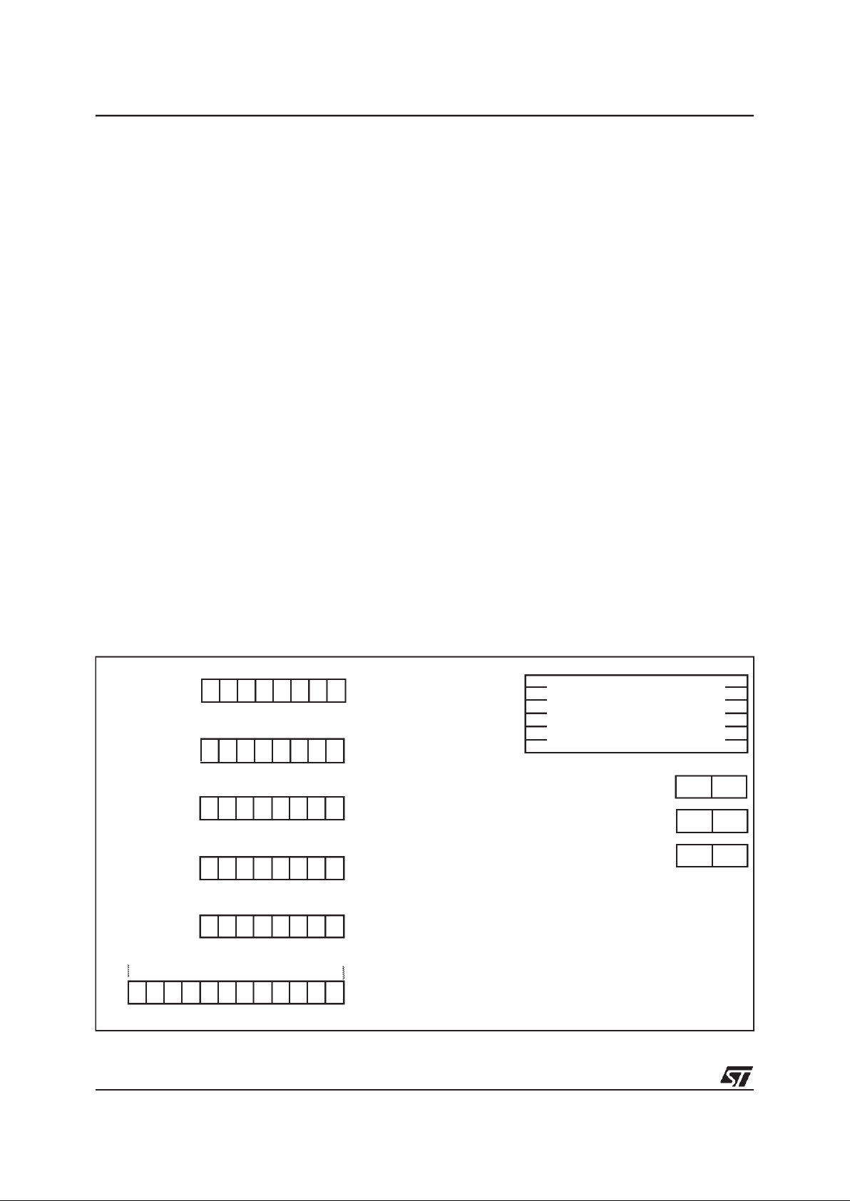
Figure 7. CPU Registers
ACCUMULATOR
X INDEX REGISTER
Y INDEX REGISTER
PROGRAM COUNTER
RESET VALUE = RESET VECTOR @ 0FFEh-0FFFh
70
70
70
0
11
RESET VALUE = xxh
RESET VALUE = xxh
RESET VALUE = xxh
x = Undefined value
V SHORT INDIRECT
70
RESET VALUE = xxh
W SHORTINDIRECT
70
RESET VALUE = xxh
NORMAL FLAGS
CN ZN
CI ZI
CNMI ZNMI
INTERRUPT FLAGS
NMI FLAGS
SIX LEVEL
STACK
REGISTER
REGISTER
1
ST6200C/ST6201C/ST6203C
17/104
CPU REGISTERS (Cont’d)
The 12-bit length allows the direct addressing of
4096 bytes in Program Space.
However, ifthe program space contains more than
4096 bytes, the additional memory in program
space can be addressed by using the Program
ROM Page register.
The PC value is incremented after reading the address of the current instruction.To execute relative
jumps, the PC and the offset are shifted through
the ALU, where they are added; the result is then
shifted back into the PC.The program counter can
be changedin the following ways:
– JP (Jump) instruction PC = Jump address
– CALL instruction PC = Call address
– Relative Branch InstructionPC = PC +/- offset
– Interrupt PC = Interrupt vector
– Reset PC = Reset vector
– RET & RETI instructions PC = Pop (stack)
– Normal instruction PC = PC + 1
Flags (C, Z). The ST6 CPU includes three pairs of
flags (Carry and Zero), each pair beingassociated
with one of the three normal modes of operation:
Normal mode, Interrupt mode and Non Maskable
Interrupt mode. Each pair consists of a CARRY
flag and a ZERO flag. One pair (CN, ZN) is used
during Normal operation, another pair is usedduring Interrupt mode (CI, ZI), and a third pair is used
in the Non Maskable Interrupt mode (CNMI, ZNMI).
The ST6 CPU uses the pair of flags associated
with the current mode: as soon as an interrupt (or
a Non Maskable Interrupt) is generated, the ST6
CPU uses the Interrupt flags (or the NMI flags) instead of the Normal flags. When the RETI instruction is executed, the previously used set of flags is
restored. It should be noted that each flag set can
only be addressed in its own context (Non Maskable Interrupt, Normal Interrupt or Main routine).
The flags are not cleared during context switching
and thus retain their status.
C : Carry flag.
This bit is set when acarry or aborrow occurs dur-
ing arithmetic operations; otherwise it is cleared.
The Carry flag is also set to the value of the bit
tested in a bit test instruction; it also participates in
the rotate left instruction.
0: No carry has occured
1: A carry has occured
Z : Zero flag
This flag is set if the result of the last arithmetic or
logical operation was equal to zero; otherwise it is
cleared.
0: The result of the last operation is different from
zero
1: The result of the last operation is zero
Switching between the three sets of flags is per-
formed automatically whenan NMI, an interrupt or
a RETI instruction occurs. As NMI mode is automatically selected after the reset of the MCU, the
ST6 core uses the NMI flags first.
Stack. The ST6 CPU includes a true LIFO (Last In
First Out) hardware stack which eliminates the
need for a stackpointer. The stack consists of six
separate 12-bit RAM locations that do not belong
to the data space RAM area. When a subroutine
call (or interrupt request) occurs, the contents of
each level are shifted into the next level down,
while the content of the PC is shifted into the first
level (the original contents of the sixth stack level
are lost). When a subroutine or interrupt return occurs (RET or RETI instructions), the first level register is shifted back into the PC and the value of
each level is popped back into the previous level.
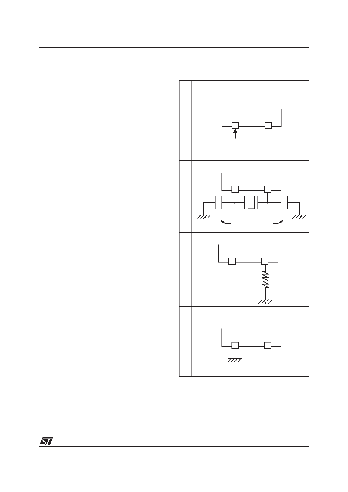
Figure 8. Stack manipulation
Since the accumulator, in common with all other
data space registers, is not stored in this stack,
management of these registers should be performed within the subroutine.
Caution: The stack will remain in its“deepest” position if more than 6 nested calls or interrupts are
executed, and consequently the last return address will be lost.
It will also remain in its highest position if the stack
is empty and a RET or RETI is executed. In this
case the next instruction will be executed.
LEVEL 1
LEVEL 2
LEVEL 3
LEVEL 4
LEVEL 5
LEVEL 6
ON
INTERRUPT,
OR
SUBROUTINE
CALL
ON RETURN
FROM
INTERRUPT,
OR
SUBROUTINE
PROGRAM
COUNTER
1
ST6200C/ST6201C/ST6203C
18/104
5 CLOCKS, SUPPLY AND RESET
5.1 CLOCK SYSTEM
The main oscillator of the MCU can be driven by
any of these clock sources:
– external clock signal
– external AT-cut parallel-resonant crystal
– external ceramic resonator
– external RC network (R
NET
).
In addition, an on-chip Low Frequency Auxiliary
Oscillator (LFAO) is available as a back-up clock
system or to reduce power consumption.
An optional Oscillator Safeguard (OSG) filters
spikes from the oscillator lines, and switches to the
LFAO backup oscillator in the event of main oscillator failure. It also automatically limits the internal
clock frequency(f
INT
) as a function of VDD, in order
to guarantee correct operation. These functions
are illustrated in Figure 10, and Figure 11.
Table 6 illustrates various possible oscillator configurations using an external crystal or ceramic
resonator, an external clock input, an external resistor (R
NET
), or the lowestcost solution using only
the LFAO.
For more details on configuring the clock options,
refer to the Option Bytes section of this document.
The internal MCU clock frequency (f
INT
) is divided
by 12 to drive the Timer, the Watchdog timer and
the A/D converter (if available), and by 13 to drive
the CPU core, as shown in Figure 9.
With an 8 MHz oscillator, the fastest CPU cycle is
therefore 1.625µs.
A CPU cycle is the smallest unit of time needed to
execute any operation (for instance, to increment
the Program Counter). An instruction may require
two, four, or five CPU cycles for execution.
Figure 9. Clock Circuit Block Diagram
MAIN
OSCILLATOR
OSG
LFAO
CORE
:13
:12
8-BIT TIMER
WATCHDOG
f
INT
OSCOFF BIT
ADC
0
1
filtering
OSCILLATOR SAFEGUARD (OSG)
OSG ENABLEOPTION BIT (See OPTION BYTE SECTION)
(ADCR REGISTER)
f
OSC
* Depending on device. See device summary on page 1.
*
*
1
ST6200C/ST6201C/ST6203C
19/104
CLOCK SYSTEM (Cont’d)
5.1.1 Main Oscillator
The oscillator configuration is specified by selecting the appropriate option in the option bytes (refer
to the Option Bytes section of this document).
When the CRYSTAL/RESONATOR option is selected, it must be used with a quartz crystal, a ceramic resonator or an external signal provided on
the OSCin pin. When theRC NETWORK option is
selected, the system clock is generated by an external resistor (the capacitor is implemented internally).
The main oscillator can be turned off (when the
OSG ENABLED option is selected) by setting the
OSCOFF bit of the ADC Control Register (not
available onsome devices). This will automatically
start the Low Frequency Auxiliary Oscillator
(LFAO).
The main oscillator can be turned off by resetting
the OSCOFFbit of the A/D Converter Control Register or by resetting the MCU. When the main oscillator starts there is a delay made up of the oscillator start-up delay period plus the duration of the
software instruction at a clock frequency f
LFAO
.
Caution: It should be noted that when the RC network option is selected, the accuracy of the frequency is about 20% so it may not be suitable for
some applications (For more details, please refer
to the Electrical Characteristics Section).
Table 6. Oscillator Configurations
Notes:
1. To select the options shown in column 1 of the above
table, refer to the Option Byte section.
2.This schematic are given for guidance only and are subject to the schematics given by the crystal or ceramic resonator manufacturer.
3. For more details, please refer to the Electrical Characteristics Section.
Hardware Configuration
Crystal/Resonator Option
1)
Crystal/Resonator Option
1)
RC Network Option
1)
OSG Enabled Option
1)
OSCin OSCout
EXTERNAL
ST6
CLOCK
NC
External Clock
OSCin OSCout
LOAD
CAPACITORS
3)
ST6
C
L2
C
L1
Crystal/Resonator Clock
2)
OSCin OSCout
ST6
R
NET
NC
RC Network
OSCin OSCout
ST6
LFAO
NC
1
ST6200C/ST6201C/ST6203C
20/104
CLOCK SYSTEM (Cont’d)
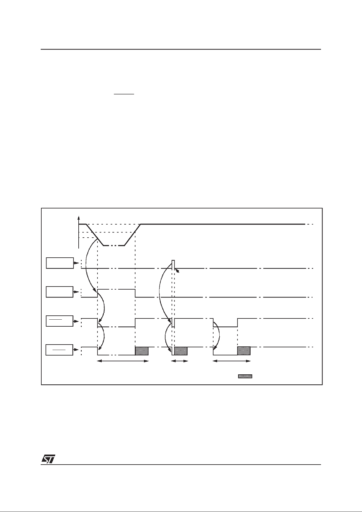
5.1.2 Oscillator Safeguard (OSG)
The Oscillator Safeguard (OSG) feature is a
means of dramatically improving the operational
integrity of the MCU. It is available when the OSG
ENABLED option is selected in the option byte (refer to the Option Bytes section of this document).
The OSG acts as a filter whose cross-over frequency is device dependent and provides three
basic functions:
– Filtering spikes on the oscillator lines which
would result in driving the CPU at excessive frequencies
– Management of the Low Frequency Auxiliary
Oscillator (LFAO), (useable as low cost internal
clock source, backup clockin case of main oscillator failure or for low power consumption)
– Automaticallylimiting thef
INT
clockfrequency as
a function of supply voltage, to ensure correct
operation even if the power supply drops.
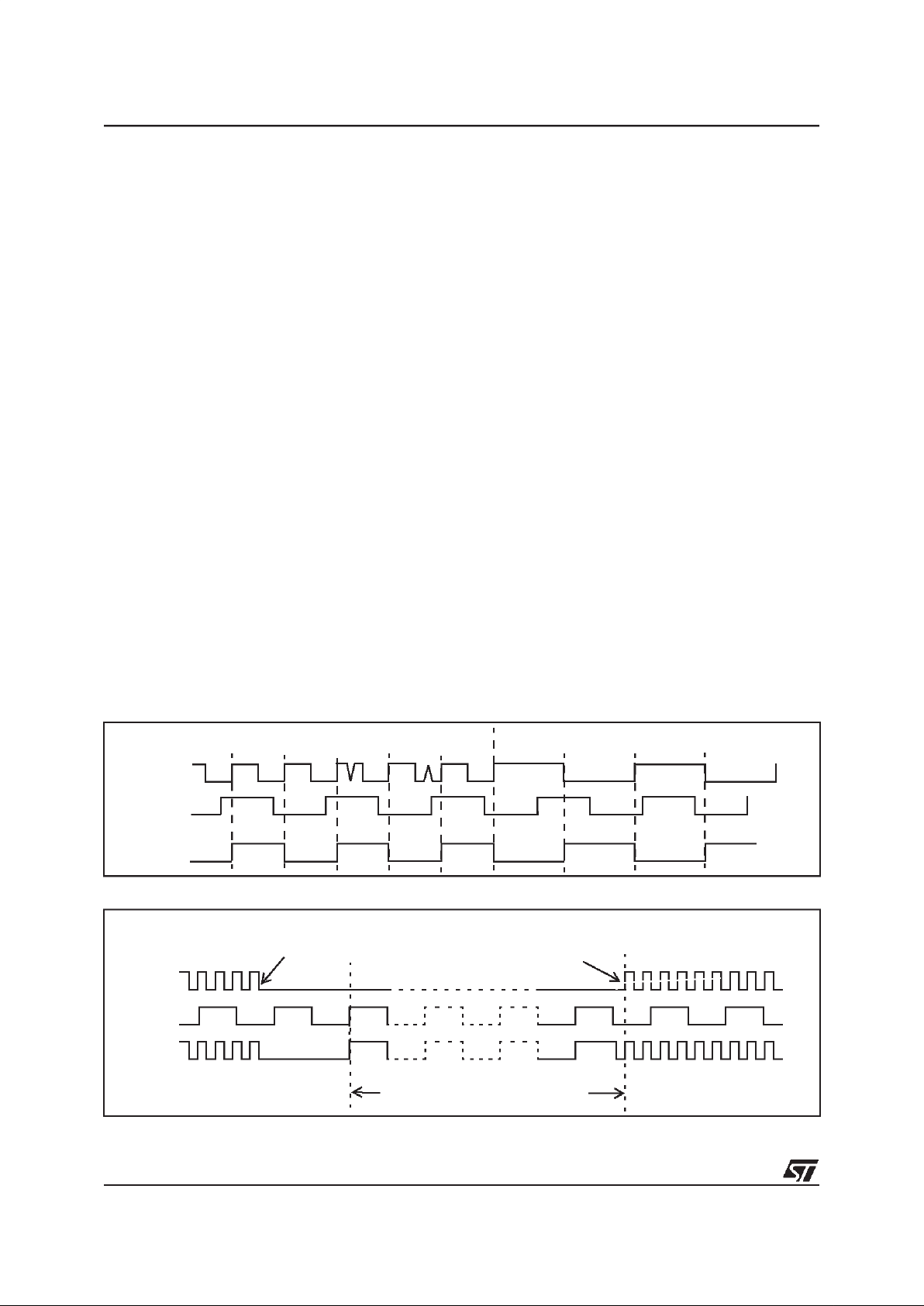
5.1.2.1 Spike Filtering
Spikes onthe oscillator lines result in an effectively
increased internal clock frequency. In the absence
of an OSG circuit, this may lead to an over frequency for a given power supply voltage. The
OSG filters out such spikes (asillustrated inFigure
10). In all cases, when theOSG isactive, the max-
imum internal clock frequency, f
INT
, is limited to
f
OSG
, which is supply voltage dependent.
5.1.2.2 Management of Supply Voltage
Variations
Over-frequency, at a given power supply level, is
seen by the OSG as spikes; it therefore filters out
some cycles in order that the internal clock frequency of the device is kept within the range the
particular device can stand (depending on VDD),
and below f
OSG
: the maximum authorised frequen-
cy with OSG enabled.
5.1.2.3 LFAO Management
When the OSG is enabled, the Low Frequency
Auxiliary Oscillator can be used (see Section
5.1.3).
Note:The OSG should be used wherever possible
as it provides maximum security for the application. It should be noted however, that it can increase power consumption and reduce the maximum operating frequency to f
OSG
(see Electrical
Characteristics section).
Caution: Care has to be taken when using the
OSG, as the internal frequency is defined between
a minimum and a maximum value and may vary
depending on bothVDDand temperature. For precise timing measurements, it is not recommended
to use the OSG.
Figure 10. OSG Filtering Function
Figure 11. LFAO Oscillator Function
f
OSC
f
OSG
f
INT
f
OSC<fOSG
f
OSC>fOSG
MAIN OSCILLATOR
STOPS
MAIN OSCILLATOR
RESTARTS
INTERNAL CLOCK DRIVEN BY LFAO
f
OSC
f
INT
f
LFAO
1

ST6200C/ST6201C/ST6203C
21/104
CLOCK SYSTEM (Cont’d)
5.1.3 Low Frequency Auxiliary Oscillator
(LFAO)
The Low Frequency Auxiliary Oscillator has three
main purposes. Firstly, it can be used to reduce
power consumption in non timing critical routines.
Secondly, it offers a fully integrated system clock,
without anyexternal components. Lastly, it acts as
a backup oscillator in case of main oscillator failure.
This oscillator is available when the OSG ENABLED option is selected in the option byte (referto
the Option Bytes section of this document). In this
case, it automatically starts one of its periodsafter
the first missing edge of the main oscillator, whatever the reason for the failure (main oscillator defective, no clock circuitry provided, main oscillator
switched off...). See Figure 11.
User code, normal interrupts, WAIT and STOP instructions, are processed as normal, at the reduced f
LFAO
frequency.The A/D converter accuracy is decreased, since the internalfrequency is below 1.2 MHz.
At power on, until the main oscillator starts, the
2048 clock cycle counter is driven by the LFAO. If
the mainoscillator starts before the 2048 cycle delay has elapsed, it takes over.
The Low Frequency Auxiliary Oscillator is automatically switched off as soon as the main oscillator starts.
5.1.4 Register Description
ADC CONTROL REGISTER (ADCR)
Address: 0D1h — Read/Write
Reset value: 0100 0000 (40h)
Bit 7:3, 1:0 = ADCR[7:3], ADCR[1:0]
ADC Control
Register
.
These bits are used to control theA/D converter (if
available on the device) otherwise they are not
used.
Bit 2 = OSCOFF
Main Oscillator Off.
0: Main oscillator enabled
1: Main oscillator disabled
Note: The OSG must be enabled using the OSGEN option in the Option Byte, otherwise the OSCOFF setting has no effect.
70
ADCR7ADCR6ADCR5ADCR4ADCR3OSC
OFF
ADCR1ADCR
0
1
ST6200C/ST6201C/ST6203C
22/104
5.2 LOW VOLTAGE DETECTOR (LVD)
The on-chip Low Voltage Detector is enabled by
setting a bit in the option bytes (refer to the Option
Bytes section of this document).
The LVD allows the device to be used without any
external RESET circuitry. In this case, the RESET
pin should be left unconnected.
If the LVD is notused, an external circuit is mandatory to ensure correct Power On Reset operation,
see figure in the Reset section. For more details,
please refer to the application note AN669.
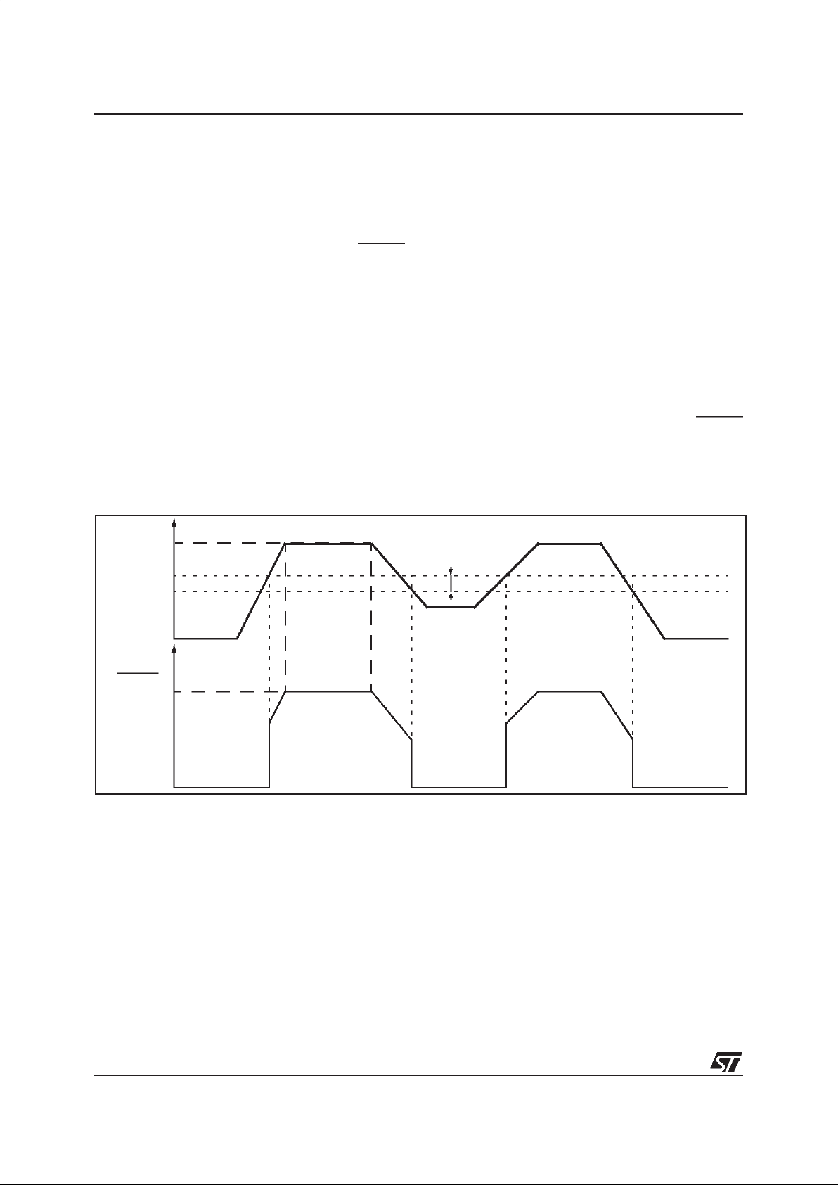
The LVD generatesa staticReset when thesupply
voltage is below a reference value. This means
that it secures the power-up as well as the powerdown keeping the ST6 in reset.
The V
IT-
referencevalue for a voltage drop is lower
than the V
IT+
reference value for power-on in order
to avoid a parasiticreset when theMCU starts running and sinks current on the supply (hysteresis).
The LVD Reset circuitry generates a reset when
VDDis below:
–V
IT+
when VDDis rising
–V
IT-
when VDDis falling
The LVD function is illustrated in Figure 12.
If the LVD is enabled, the MCU can be in only one
of two states:
– Overthe input thresholdvoltage, it is running un-
der full software control
– Below the input threshold voltage, it is in static
safe reset
In these conditions, secure operation is guaranteed without the need for external reset hardware.
During a Low Voltage Detector Reset, the RESET
pin is held low, thus permitting the MCU to reset
other devices.
Figure 12. Low Voltage Detector Reset
V
DD
V
IT+
RESET
V
IT-
V
hyst
1
ST6200C/ST6201C/ST6203C
23/104
5.3 RESET
5.3.1 Introduction
The MCU can be reset in three ways:
■ A low pulse input on the RESET pin
■ Internal Watchdog reset
■ Internal Low Voltage Detector (LVD) reset
5.3.2 RESET sequence
The basic RESET sequence consists of 3 main
phases:
■ Internal (watchdog or LVD) or external Reset
event
■ A delay of 2048 clock (f
INT
) cycles
■ RESET vector fetch
The 2048 clock cycle delay allows the oscillator to
stabilise and ensures that recovery has taken
place from the Reset state.
The RESET vector fetch phase duration is 2 clock
cycles.
When a reset occurs:
– The stack is cleared
– The PC is loaded with the address of the Reset
vector. It is located in program ROM starting at
address 0FFEh.
A jump to the beginning of the user program must
be coded at this address.
– Theinterrupt flagis automatically set,so that the
CPU is in Non Maskable Interrupt mode. This
prevents the initialization routine from being interrupted. The initialization routine should therefore beterminated by a RETIinstruction, inorder
to go back to normal mode.
Figure 13. RESET Sequence
V
DD
RESET PIN
WATCHDOG
V
IT+
V
IT-
WATCHDOG UNDERFLOW
RESET
2048 CLOCK CYCLE (f
INT
) DELAY
LVD
RESET
INTERNAL
RUN
RESET
RUN RUN RUN
RESET RESET
RESET
1
ST6200C/ST6201C/ST6203C
24/104
RESET (Cont’d)
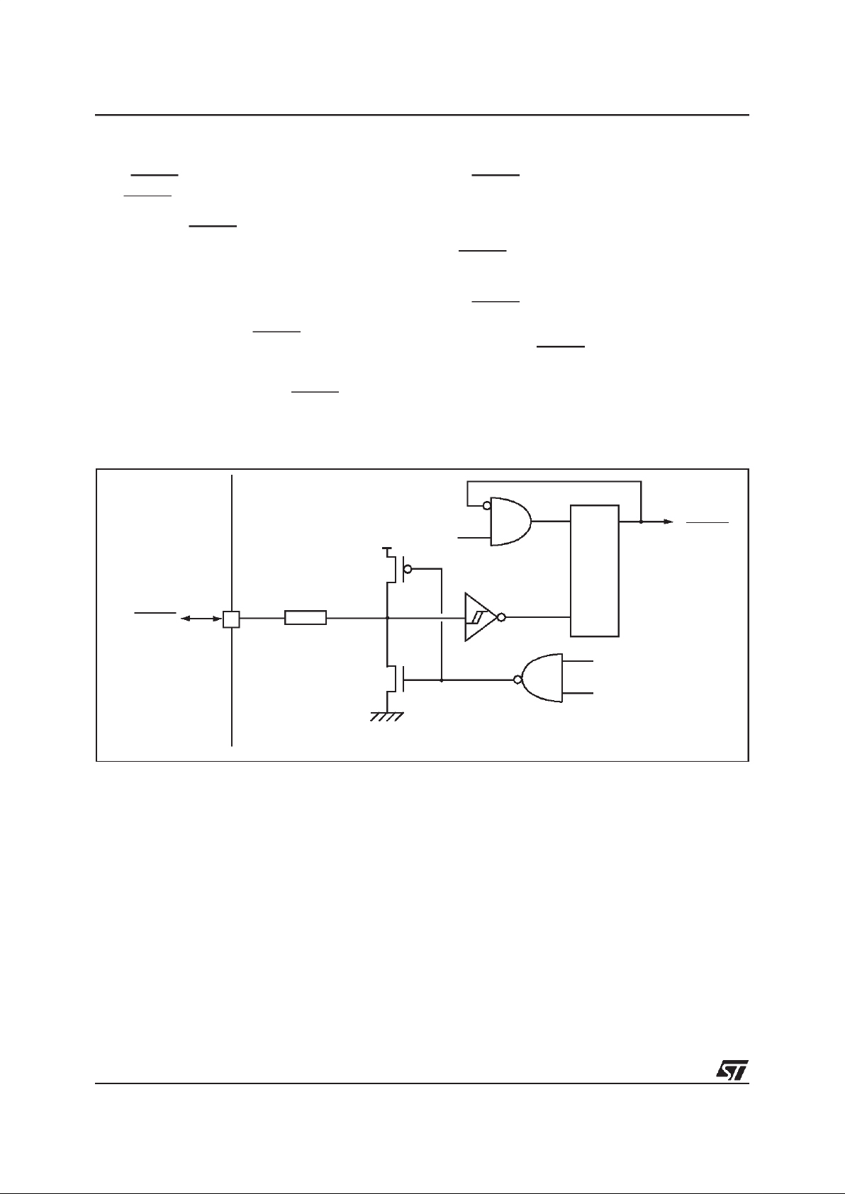
5.3.3 RESET Pin
The RESET pin may be connected to a device on
the application board in order to reset the MCU if
required. The RESET pin may be pulled low in
RUN, WAIT or STOP mode. This input can be
used toreset the internal state of the MCU and ensure it starts-up correctly. The pin, which is connected toan internal pull-up, is active low and features a Schmitt trigger input. A delay (2048 clock
cycles) added to the external signal ensures that
even short pulses on the RESET pin are accepted
as valid, provided VDDhas completed its rising
phase and that the oscillator is running correctly
(normal RUN or WAIT modes). The MCU is kept in
the Reset state as long as the RESET pin is held
low.
If the RESET pin is grounded while the MCU is in
RUN or WAIT modes, processing of the user program is stopped (RUN mode only), the I/O ports
are configured as inputs with pull-up resistors and
the main oscillator is restarted. When the level on
the RESET pinthen goes high, the initializationsequence is executed at the end of the internal delay
period.
If the RESET pin is grounded while the MCU is in
STOP mode, the oscillator startsup and all the I/O
ports are configured as inputs with pull-up resistors. When the RESET pin level then goes high,
the initialization sequence is executed at the end
of the internal delay period.
A simple external RESET circuitry isshown in Figure 15. For more details, please refer to the application note AN669.
Figure 14. Reset Block Diagram
f
INT
COUNTER
RESET
WATCHDOG RESET
LVD RESET
INTERNAL
RESET
R
ESD
1)
1) Resistive ESD protection
V
DD
R
PU
2048 clock cycles
1
ST6200C/ST6201C/ST6203C
25/104
RESET (Cont’d)
5.3.4 Watchdog Reset
The MCU provides a Watchdog timer function in
order to be able to recover from software hangups. If the Watchdog register is not refreshed before an end-of-count condition is reached, a
Watchdog reset is generated.
After a Watchdog reset, the MCU restarts in the
same way as if a Reset was generated by the RESET pin.
Note: When a watchdog reset occurs, the RESET
pin is tied low for very short time period, to flag the
reset phase. This time is not long enough to reset
external circuits.
For more details refer to the Watchdog Timer
chapter.
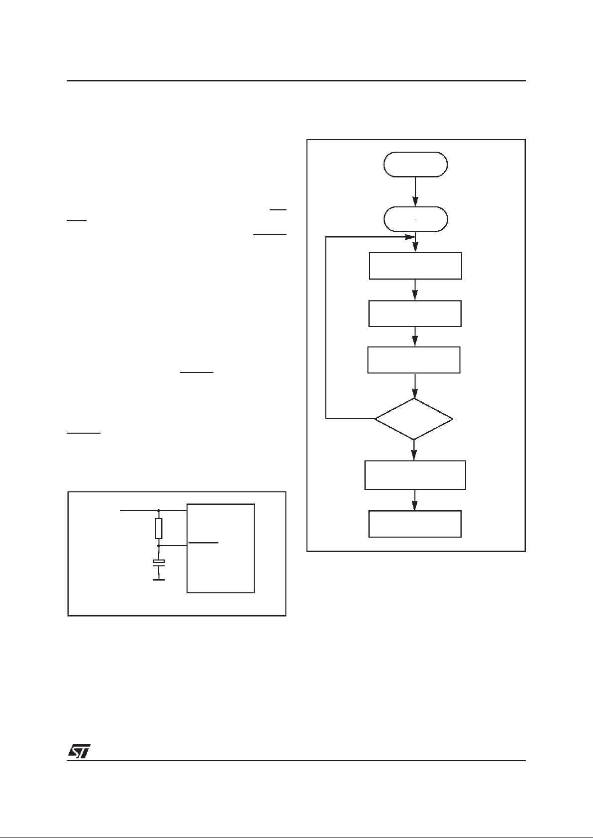
5.3.5 LVD Reset
Two different RESET sequences caused bythe internal LVD circuitry can be distinguished:
■ Power-On RESET
■ Voltage Drop RESET
During an LVD reset, the RESET pin is pulled low
when VDD<V
IT+
(rising edge) or VDD<V
IT-
(falling
edge).
For more details, refer to the LVD chapter.
Caution: Do not externally connect directly the
RESET pin to VDD, this may cause damage to the
component in case of internal RESET (Watchdog
or LVD).
Figure 15. Simple external Reset Circuitry
Figure 16. Reset Processing
ST62xx
RESET
V
DD
V
DD
R
C
Typical: R = 10K
C = 10nF
R > 4.7 K
INT LATCH CLEARED
NMI MASK SET
(IF PRESENT)
SELECT
NMI MODE FLAGS
IS RESET STILL
PRESENT?
YES
PUT FFEh
ON ADDRESS BUS
FROM RESET LOCATIONS
FFEh/FFFh
NO
FETCH INSTRUCTION
LOAD PC
INTERNAL
RESET
RESET
2048
CLOCK CYCLE
DELAY
1
ST6200C/ST6201C/ST6203C
26/104
6 INTERRUPTS
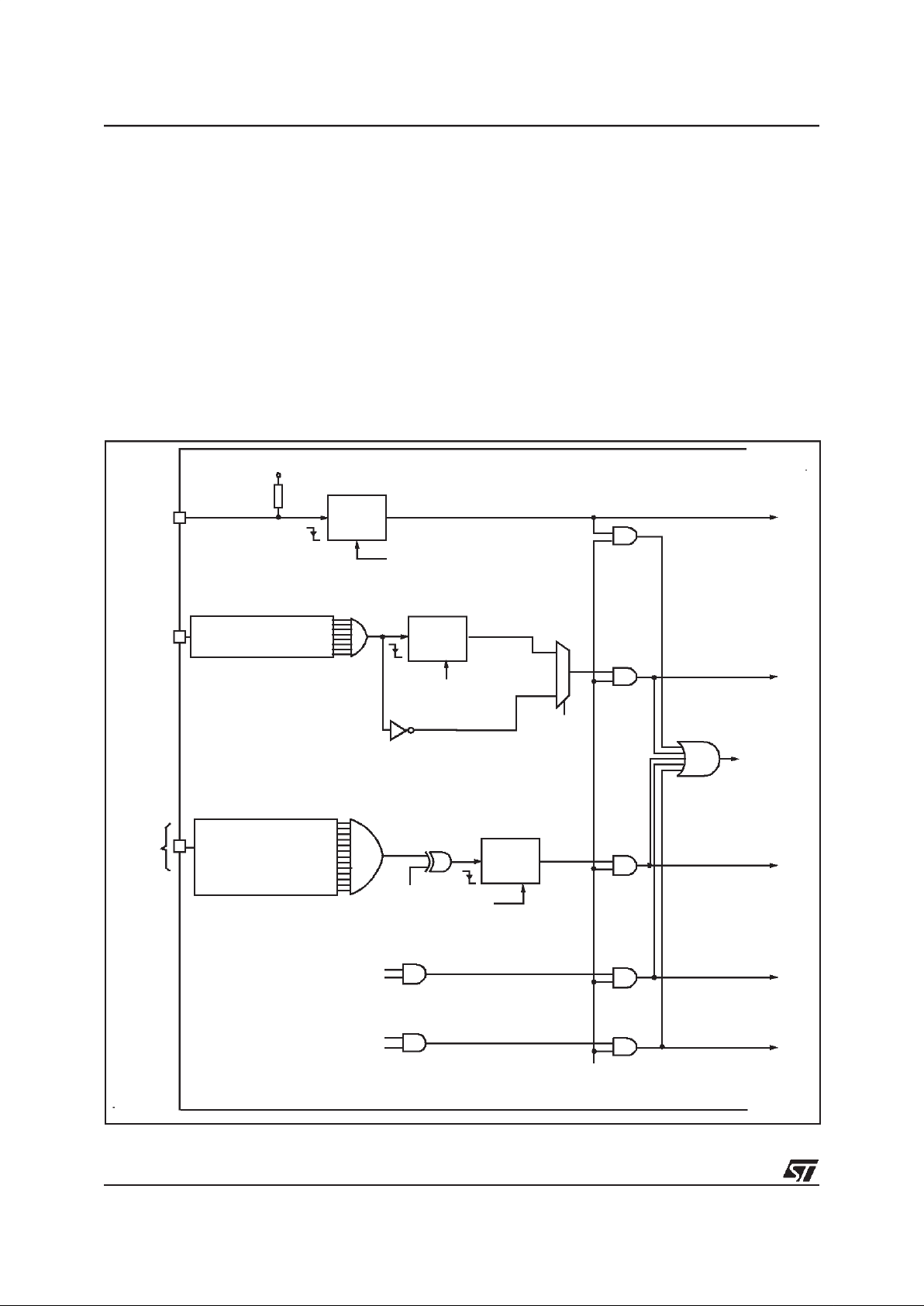
The ST6 core may be interrupted by four maskable interrupt sources, in addition to a Non Maskable Interrupt (NMI) source. The interrupt processing flowchartis shown in Figure 18.
Maskable interrupts must be enabled by setting
the GEN bit in the IOR register. However, even if
they are disabled (GEN bit = 0), interrupt events
are latchedand may be processed as soon as the
GEN bit is set.
Each source is associated with a specific Interrupt
Vector, locatedin Program space (seeTable 8). In
the vector location, the user must write a Jump in-
struction to the associated interrupt service routine.
When an interrupt source generates an interrupt
request, the PC register is loaded with the address
of the interrupt vector, which then causes a Jump
to the relevant interrupt service routine, thus servicing the interrupt.
Interrupt are triggered byevents either on external
pins, or from the on-chip peripherals. Several
events can be ORed on the same interrupt vector.
On-chip peripherals have flag registers to determine which event triggered the interrupt.
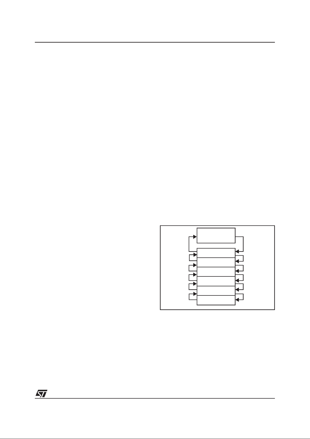
Figure 17. Interrupts Block Diagram
NMI
ESB BIT
V
DD
LATCH
CLEARED BY H/W
AT START OF VECTOR #0 ROUTINE
VECTOR #0
LES BIT
1
0
LATCH
CLEARED BY H/W
AT START OF
VECTOR #1
VECTOR#2
VECTOR #3
VECTOR #4
LATCH
CLEARED
BY H/W AT START OF
VECTOR #2 ROUTINE
I/O PORT REGISTER
CONFIGURATION
“INPUT WITH INTERRUPT”
I/O PORT REGISTER
CONFIGURATION
“INPUT WITH INTERRUPT”
EXIT FROM
STOP/WAI T
VECTOR #1 ROUTINE
TIMER
A/D CONVERTER *
TMZ BIT
ETI BIT
EAI BIT
EOC BIT
GEN BIT
PB0..PB1
PA1..PA3
(TSCR REGISTER)
(ADCR REGISTER)
(IOR REGISTER)
(IOR REGISTER)
(IOR REGISTER)
PB3
PB5..PB7
* Depending on device. See device summary on page 1.
1

ST6200C/ST6201C/ST6203C
27/104
6.1 INTERRUPT RULES AND PRIORITY
MANAGEMENT
■ A Reset can interrupt the NMI and peripheral
interrupt routines
■ The Non Maskable Interrupt request has the
highest priority and can interrupt any peripheral
interrupt routine at any time but cannot interrupt
another NMI interrupt.
■ No peripheral interrupt can interrupt another. If
more than one interrupt request is pending,
these are processed by the processor core
according to their priority level: vector#1 has the
highest priority while vector #4 the lowest. The
priority of each interrupt source is fixed by
hardware (see Interrupt Mapping table).
6.2 INTERRUPTS AND LOW POWER MODES
All interrupts cause the processor to exit from
WAIT mode. Only the external and some specific
interrupts from the on-chip peripherals cause the
processor to exit from STOP mode (refer to the
“Exit from STOP“ column in the Interrupt Mapping
Table).
6.3 NON MASKABLE INTERRUPT
This interrupt is triggered when a falling edge occurs on the NMI pin regardless of the state of the
GEN bit in the IOR register. An interrupt request
on NMI vector #0 is latched by a flip flop which is
automatically reset by the core at the beginning of
the NMI service routine.
6.4 PERIPHERAL INTERRUPTS
Different peripheral interrupt flags in the peripheral
control registers are able to cause an interrupt
when they are active if both:
– The GEN bit of the IOR register is set
– Thecorresponding enable bit is set in the periph-
eral control register.
Peripheral interrupts are linked to vectors #3 and
#4. Interrupt requests are flagged by a bit in their
corresponding control register. This means that a
request cannot be lost, because the flag bit must
be cleared by user software.
1

ST6200C/ST6201C/ST6203C
28/104
6.5 EXTERNAL INTERRUPTS (I/O Ports)
External interrupt vectors can be loaded into the
PC register if the corresponding external interrupt
occurred and if the GEN bit is set. These interrupts
allow the processor to exit from STOP mode.
The external interrupt polarity is selected through
the IOR register.
External interrupts are linked to vectors #1 and #
2.
Interrupt requests on vector #1 can be configured
either as edge or level-sensitive using the LES bit
in the IOR Register.
Interrupt requests from vector #2 are always edge
sensitive. The edge polarity can be configured using the ESB bit in the IOR Register.
In edge-sensitive mode, a latch is set when a edge
occurs on the interrupt source line and is cleared
when the associated interrupt routine is started.
So, an interrupt request can be stored until completion of the currently executing interrupt routine,
before being processed. If several interrupt requests occurs before completion of the current interrupt routine, only the first request is stored.
Storing ofinterrupt requests is not possible in level
sensitive mode. To be taken into account, the low
level must be present on the interrupt pin when the
MCU samples the line after instruction execution.
6.5.1 Notes on using External Interrupts
ESB bit Spurious Interrupt on Vector #2
If a pin associated with interrupt vector #2 is configured as interrupt with pull-up, whenever vector
#2 is configured tobe rising edge sensitive (by setting the ESB bit in the IOR register), an interrupt is
latched although a rising edge may not have occured on the associated pin.
This is due to the vector #2 circuitry.The workaround is to discard this first interrupt request in the
routine (using a flag for example).
Masking of One Interrupt by Another on Vector
#2.
When two or moreport pins (associated with interrupt vector #2) are configured together as input
with interrupt (falling edge sensitive), as long as
one pin is stuck at ’0’,the other pin cannever generate an interrupt even if an active edge occurs at
this pin. The same thing occurs when one pin is
stuck at ’1’and interrupt vector #2 is configured as
rising edge sensitive.
To avoid this the first pin must input a signal that
goes back upto ’1’ right after the falling edge. Otherwise, in the interrupt routine for the first pin, deactivate the “input with interrupt” mode using the
port control registers (DDR, OR, DR). An active
edge on another pin can then be latched.
I/O port Configuration Spurious Interrupt on
Vector #2
If a pin associated with interrupt vector #2 is in ‘input with pull-up’ state, a ‘0’ level is present on the
pin and the ESB bit= 0, when the I/O pin is configured as interrupt with pull-up by writing to the
DDRx, ORx and DRx register bits, an interrupt is
latched although a falling edge may not have occurred on the associated pin.
In the opposite case, if the pin is in interrupt with
pull-up state , a 0 level is present on the pin and
the ESB bit =1, when the I/O port is configured as
input with pull-up by writing to the DDRx, ORxand
DRx bits, an interrupt is latched although a rising
edge may not have occurred on the associated
pin.
1
ST6200C/ST6201C/ST6203C
29/104
6.6 INTERRUPT HANDLING PROCEDURE
The interrupt procedure isvery similar to a callprocedure, in fact the user can consider the interrupt
as an asynchronous call procedure. As this is an
asynchronous event, the user cannot know the
context and the time at which it occurred. As a result, the user should save all Data space registers
which may be used within the interrupt routines.
The following list summarizes the interrupt procedure:
When an interrupt request occurs, the following
actions are performed by the MCU automatically:
– The core switches from the normal flags to the
interrupt flags (or the NMI flags).
– ThePC contents arestored inthe top level ofthe
stack.
– The normal interrupt lines are inhibited (NMI still
active).
– The internal latch (if any) is cleared.
– TheassociatedinterruptvectorisloadedinthePC.
When an interrupt request occurs, the following
actions must be performed by the user software:
– User selected registers have to be saved within
the interrupt service routine (normally ona soft-
ware stack).
– The source of the interrupt must be determined
by polling the interrupt flags (if more than one
source is associated with the same vector).
– The RETI (RETurn from Interrupt) instruction
must end the interrupt service routine.
After the RETI instruction isexecuted, the MCU re-
turns to the main routine.
Caution: When a maskable interrupt occurs while
the ST6 core is in NORMAL mode and during the
execution of an “ldi IOR, 00h”instruction (disabling
all maskable interrupts): if the interrupt request occurs during the first 3 cycles of the “ldi” instruction
(which is a 4-cycle instruction) the core will switch
to interrupt mode BUT the flags CN and ZN will
NOT switch to the interrupt pair CI and ZI.
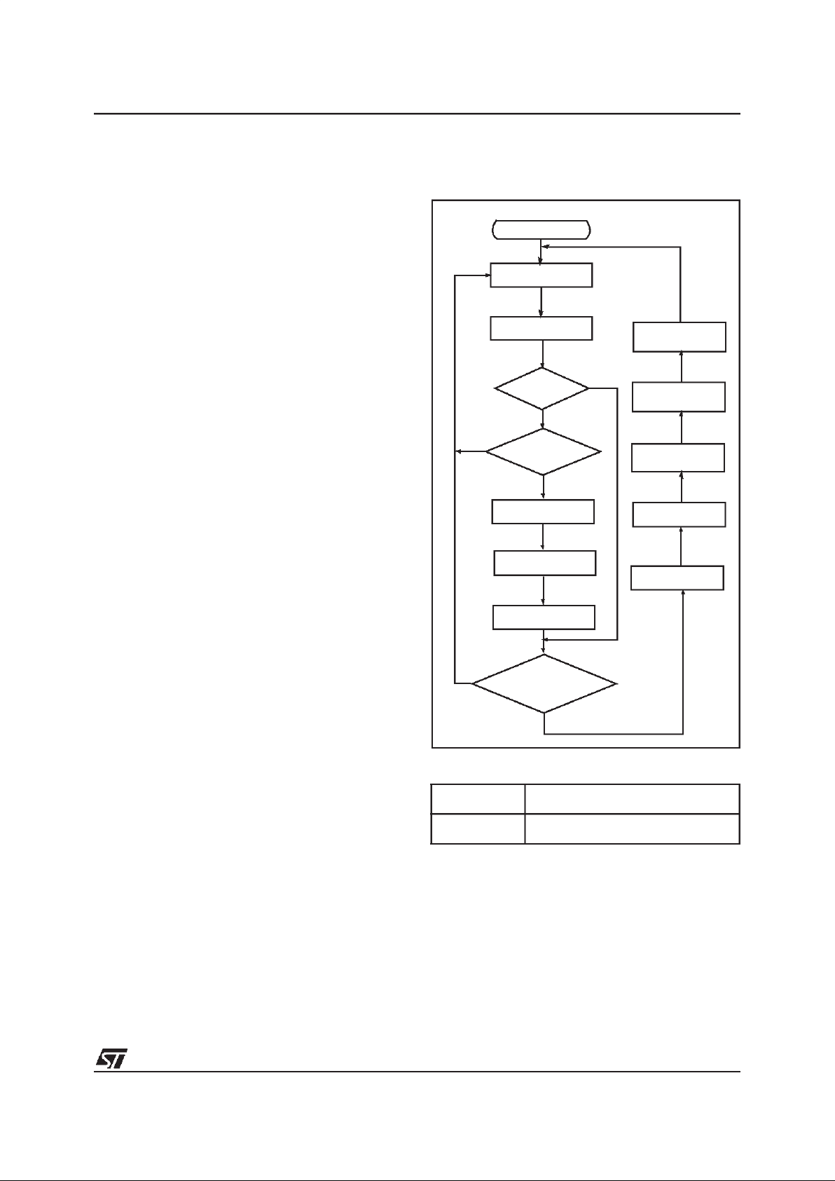
6.6.1 Interrupt Response Time
This is defined as the time between the moment
when the Program Counter is loaded with the interrupt vector and when the program has jump to
the interrupt subroutine and is ready to execute
the code. It depends on when the interrupt occurs
while the core is processing an instruction.
Figure 18. Interrupt Processing Flow Chart
Table 7. Interrupt Response Time
One CPU cycle is 13 external clock cycles thus 11
CPU cycles = 11 x (13 /8M) = 17.875 µs with an 8
MHz external quartz.
Minimum 6 CPU cycles
Maximum 11 CPU cycles
INSTRUCTION
FETCH
INSTRUCTION
EXECUTE
INSTRUCTION
WAS
THE INSTRUCTION
A RETI?
ENABLE
MASKABLE INTERRUPTS
SELECT
NORMAL FLAGS
“POP”
THE STACKED PC
IS THERE AN
AN INTERRUPT REQUEST
AND INTERRUPT MASK?
SELECT
INTERRUPT FLAGS
PUSH THE
PC INTO THE STACK
LOAD PC FROM
INTERRUPT VECTOR
DISABLE
MASKABLE INTERRUPT
NO
NO
YES
IS THE CORE
ALREADY IN
NORMAL MODE?
YES
NO
YES
CLEAR
INTERNAL LATCH
*)
*)
If a latch is present on the interrupt source line
1
ST6200C/ST6201C/ST6203C
30/104
6.7 REGISTER DESCRIPTION
INTERRUPT OPTION REGISTER (IOR)
Address: 0C8h — Write Only
Reset status: 00h
Caution: This register is write-only and cannot be
accessed by single-bit operations (SET, RES,
DEC,...).
Bit 7 =Reserved, must be cleared.
Bit 6 = LES
Level/Edge Selection bit
.
0: Falling edge sensitivemode is selected for inter-
rupt vector #1
1: Low level sensitive mode is selected for inter-
rupt vector #1
Bit 5 = ESB
Edge Selection bit
.
0: Falling edge mode on interrupt vector #2
1: Rising edge mode on interrupt vector #2
Bit 4 = GEN
Global Enable Interrupt
.
0: Disable all maskable interrupts
1: Enable all maskable interrupts
Note: When the GEN bit iscleared, the NMI interrupt isactive but cannot be used toexit from STOP
or WAIT modes.
Bits 3:0 = Reserved, must be cleared.
Table 8. Interrupt Mapping
* Depending on device. See device summary on page 1.
70
- LES ESB GEN - - - -
Vector
number
Source
Block
Description
Register
Label
Flag
Exit
from
STOP
Vector
Address
Priority
Order
RESET Reset N/A N/A yes FFEh-FFFh
Vector #0 NMI Non Maskable Interrupt N/A N/A yes FFCh-FFDh
NOT USED
FFAh-FFBh
FF8h-FF9h
Vector #1 Port A Ext. Interrupt Port A N/A N/A yes FF6h-FF7h
Vector #2 Port B Ext. Interrupt Port B N/A N/A yes FF4h-FF5h
Vector #3 TIMER Timer underflow TSCR TMZ yes FF2h-FF3h
Vector #4 ADC * End Of Conversion ADCR EOC no FF0h-FF1h
Priority
Lowest
Highest
Priority
1
 Loading...