

SGS Thomson Microelectronics ST3384ECDR, ST3384ECD, ST3384EBPR, ST3384EBDR, ST3384EBD Datasheet
±15KV ESD-PROTECTED, 3 TO 5.5V, LOW POWER,
UP TO 250KBPS, RS-232 TRANSCEIVER
■ ESD PROTECTIO FOR RS-232I/O PINS
±15KV (HUMAN BODY MODEL)
■ LATCHUP FREE
■ 1µA LOW P OWER SHUTDOWN
■ 300µA SUP PLY CURRE NT
■ 250Kbps GUARENTEED DATA RATE
■ 20µs TYPICAL TIME TO EXIT SHUTDOWN
■ 6V/µs G UARANTEED SLEW RATE
■ MEET EIA/TIA-232 SPECIFICATIONSDOWN
TO 3V
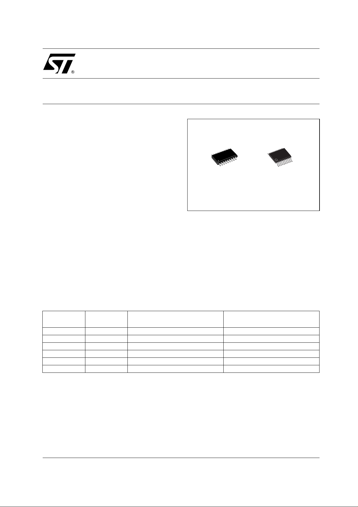
■ PACKAGES: SO-18 AND SSOP-20
DESCRIPTION
The S T3384E is a 3V powered EIA/TIA-232 and
V.28/V.24 communications interface with low
power requirements, high data-rate capabilities
and enhanced electrostatic discharge (ESD)
protection. All transmitter outputs and receiver
inputs are protected to ±15kV using the Human
Body Model. The ST3384E has a proprietary low
dropout transmitter output stage enabling true
RS-232 performance from 3 to 5.5V supplies with
a dual charge pump. The charge pump require
only four small 0.1µF external capacitors for
operation from a 3.3V supply.
ST3384E
SO-18 SSOP20
The device is guaranteed to run at data rates of
250Kbps while maintaining RS-232 output levels.
The ST3384E has two receive rs and two drivers. It
features a 1µA shutdown mode that reduces
power consumption and ext ends battery life in
portable systems.
Typical applications are in Notebook,
Sub-notebook, and Palmtop Computers, Battery
Powered Equipment, Hand-Held Equipment,
Peripherals, Printers.
ORDERING CODES
Type
ST3384ECD 0 to 70 °C SO-18 (Tube) 50 parts per tube / 20 tube per box
ST3384EBD -40 to 85 °C SO-18 (Tube) 50 parts per tube / 20 tube per box
ST3384ECDR 0 to 70 °C SO-18 (Tape & Reel) 1000 parts per reel
ST3384EBDR -40 to 85 °C SO-18 (Tape & Reel) 1000 parts per reel
ST3384ECPR 0 to 70 °C SSOP20 (Tape & Reel) 1350 parts per reel
ST3384EBPR -40 to 85 °C SSOP20 (Tape & Reel) 1350 parts per reel
Temperature
Range
Package Comments
1/11July 2003

ST3384E
PIN CONFIGURATION
PIN DESCRIPTION
SO-18 SSOP20
PlN N°
(SO-18)
PlN N°
(SSOP20)
SYMBOL NAME AND FUNCTION
1 1, 10, 11 N.C. Not Connected
22
+
C
1
Positive Terminal for the first Charge Pump
Capacitor
3 3 V+ 5.5V Generated By The Charge Pump
44
55
66
-
C
1
+
C
2
-
C
2
Negative Terminal for the first Charge Pump
Capacitor
Positive Terminal for the second Charge Pump
Capacitor
Negative Terminal for the second Charge Pump
Capacitor
7 7 V- -5.5V Generated By The Charge Pump
88
99
10 12
11 13
12 14
13 15
14 16
15 17
T2
R2
R1
T1
R2
T2
T1
R1
OUT
IN
OUT
IN
IN
OUT
IN
OUT
Second Transmitter Output Voltage
Second Receiver Input Voltage
Second Receiver Output Voltage
Second Transmitter Input Voltage
First Transmitter Input Voltage
First Receiver Output Voltage
First Receiver Input Voltage
First Transmitter Output Voltage
16 18 GND Ground
17 19
V
CC
18 20 SHDN
3V to 5.5V Supply Voltage. Connect a 0.1µF
capacitor to GND
Active Low Shutdown Control Input. Drive Low To
Shut-down Transmitters, receiver and Charge
Pump
2/11
ST3384E
ABSOLUTE MAXIMUM RATINGS
Symbol Parameter Value Unit
V
V+
V- Inverted Voltage Terminal (V- to GND) (Note 1) 0.3 to -7 V
V+ +|V-| (Note 1) 13 V
T
SHDN
R
T
OUT
R
OUT
t
SHORT
Absolute Maximum Ratings are those values beyond which damage to the device may occur. Functional operation under these condition is
not implied. V+ and V- can have a maximum magnitude of +7V, but their absolute addition cannot exceed 13 V.
Note 1: V+ and V- can have maximum magnitude of 7V, but their absolute difference cannot exceed 13V.
SHUTDOWN TRUTH TABLE
Supply Voltage (VCCto GND)
CC
Doubled Voltage Terminal (V+ to GND) (Note 1) (V
Transmitter Input Voltage
IN
-0.3 to 6 V
-0.3)to7
CC
-0.3 to 6 V
Shutdown Input Voltage (SHDN to GND) -0.3 to 6 V
Receiver Input Voltage (RINto GND)
IN
Transmitter Output Voltage (T
OUT
to GND)
± 25 V
± 13.2 V
Receiver Output Voltage -0.3 to (VCC+ 0.3)
Transmitter Output Short to GND Time
Continuous
V
V
SHDN
T-OUT R-OUT
L High Z High Z
H Active Active
ELECTRICAL CHARACTERISTICS
(C
±10% -40°C < T
Symbol Parameter Test Conditions Min. Typ. Max. Unit
=0.1µF, VCC= 3V to 5.5V, tested at 3.3V ±10% C1= 0.047µF, C2-C4=0.33µFtestedat5V
1-C4
< 85°C unl es s otherwise noted. Typical values are referred to TA= 25°C)
A
I
VCCPower Supply Current SHDN = NO LOAD 0.3 1 mA
CC
I
SHDN
SHUTDOWN Supply
Current
ESD R-IN, T-OUT Electrostatic
SHDN =GND 1 10 µA
Human Body Model ±15 kV
Discharge Immunity
LOGIC INPUT ELECTRICAL CHARACTERISTICS
(C
±10% -40°C < T
Symbol Parameter Test Conditions Min. Typ. Max. Unit
=0.1µF, VCC= 3V to 5.5V, tested at 3.3V ±10% C1= 0.047µF, C2-C4=0.33µFtestedat5V
1-C4
< 85°C unl es s otherwise noted. Typical values are referred to TA= 25°C)
A
Input Logic Threshold Low T-IN, SHDN 0.8 V
V
IL
Input Logic Threshold High T-IN, SHDN VCC= 3.3V 2 V
V
IH
T-IN, SHDN
V
Transmitter Input
HYS
Hysteresis
Input Leakage Current T-IN, SHDN ± 0.01 ± 1 µA
I
IL
VCC= 5.0V 2.4
0.5 V
3/11
ST3384E
TRANSMITTER ELECTRICAL CHARACTERISTICS
(C
±10% -40°C < T
Symbol Parameter Test Conditions Min. Typ. Max. Unit
V
R
RECEIVER DC TARGET ELECTRICAL CHARACT ERISTICS
(C
±10% -40°C < T
Symbol Parameter Test Conditions Min. Typ. Max. Unit
=0.1µF, VCC= 3V to 5.5V, tested at 3.3V ±10% C1= 0.047µF, C2-C4=0.33µFtestedat5V
1-C4
< 85°C unl es s otherwise noted. Typical values are referred to TA= 25°C)
A
TOUT
TOUT
I
TSC
I
TOL
Output Voltage Swing All Transmitter outputs loaded with 3 KΩ
to GND
Transmitter Output
Resistance
VCC=V+=V-=0V
Transmitter output = ± 2V
Output Short Circuit Current ± 50 mA
Output Leakage Current VCC= 0V or 3V to 5.5V V
OUT
= ± 12V
± 5 ± 5.4 V
300 10M Ω
Transmitters Disabled
=0.1µF, VCC= 3V to 5.5V, tested at 3.3V ±10% C1= 0.047µF, C2-C4=0.33µFtestedat5V
1-C4
I
OL
V
RIN
V
RIL
V
RITH
V
RIH
R
RIN
V
ROL
V
ROH
Output Leakage Current R-OUT, Receiver Disabled ± 0.05 ± 10 µA
Input Voltage Operating
Range
Input Threshold Low TA= 25°C VCC= 3.3V 0.6 1.2 V
Input Threshold High TA= 25°C VCC= 3.3V 1.5 2.4 V
Input Hysteresis 0.5 V
Input Resistance TA= 25°C 3 5 7 KΩ
TTL/CMOS Output Voltage
Low
TTL/CMOS Output Voltage
High
< 85°C unl es s otherwise noted. Typical values are referred to TA= 25°C)
A
-25 ± 25 V
= 25°C VCC= 5.5V 0.8 1.5
T
A
= 25°C VCC= 5.5V 1.8 2.4
T
A
I
= 2 mA 0.4 V
OUT
I
=-1mA VCC-0.6 VCC-0.1 V
OUT
± 25 µA
TIMING TARGET ELECTRICAL CHARACTER ISTICS
(C
±10% -40°C < T
Symbol Parameter Test Conditions Min. Typ. Max. Unit
-t
|t
-t
(Note 1) Transmitter Skew is measured at the transmitter zero cross points.
4/11
=0.1µF, VCC= 3V to 5.5V, tested at 3.3V ±10% C1= 0.047µF, C2-C4=0.33µFtestedat5V
1-C4
< 85°C unl es s otherwise noted. Typical values are referred to TA= 25°C)
A
Maximum Data Rate RL=3KΩ CL2= 1000pF
D
R
250 Kbps
one transmitter switching
t
PHLR
t
PLHR
|t
PHLT
PLHT
PHLR
PLHR
t
EX
S
Receiver Propagation Delay R
Transmitter Propagation
Delay Difference (Note 1)
|
Receiver Propagation Delay
Difference
|
Time to Exit Shutdown V
Transition Slew Rate TA= 25°C RL=3KΩto 7KΩ VCC= 3.3V
RT
XIN
to R
XOUT
CL= 150pF 0.15 µs
(Note 1) 150 ns
100 ns
OUT
≥ 3V, R
at V+ = 3 KΩ 20 µs
LOAD
Measured from +3V to -3V or -3V to +3V
= 150pF to 1000pF
C
L
C
= 150pF to 2500pF
L
6
4
8
8
30
30
V/µs
V/µs
 Loading...