ST1305
High Endurance CMOS 192 bit EEPROM
With Secure Logic Access Control
BRIEF DATA
■
Single 5 V Supply Voltage
■
Programming Time: 5 ms
■
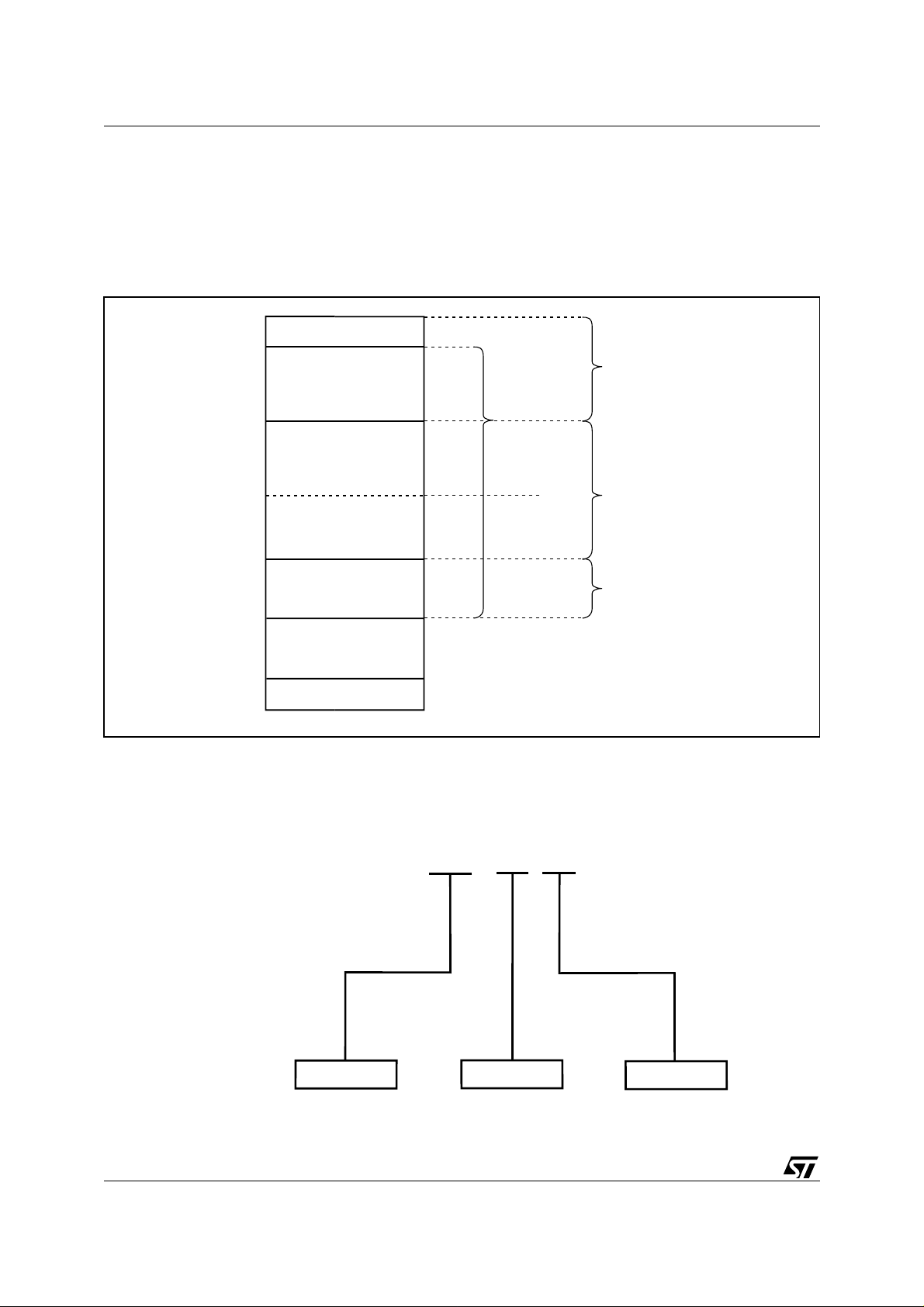
Memory Divided Into:
– 16 bits of Circuit Identification
– 48 bits of Card Identification
– 48 bits of Count Data
– 16 bits of Certificate
– 48 bits of Transport Code
– 64 bits of Issuer Data
■
Counting Capability up to 262,144 Units
■
Circuit Protected by Transport Code for Delivery
from ST to the Customer
■
5 External Contacts Only (ISO 7816 Compatible)
■
Answer to Reset (Fully Compatible with ISO 7816-3)
■
E.S.D. Protection Greater Than 4000 V
■
Power-On and Low VCC Reset
■
10 Years Data Retention
■
1 Million Erase/Write Cycles Endurance
DESCRIPTION
The ST1305 is a 192-bit EEPROM device with associated security logic to control memory access. The circuit
includes counting capabilities and thus is very well
adapted to prepaid card applications.
The ST1305 is protected by hard-wired security logic
and special fuses. The memory is arranged as a m at rix
of 24x8 cells, accessed in a serial bit-wise fashion for
reading and programming, and in a byte-wise fashion
for internal erasing.
The device recognises t hree comm ands issue d via the
RST and CLK pins (as described in the full data sheet):
– RESET: to reset the internal address register to 00d
– READ: to increment the internal address register,
and read the data bit at that address
– PROG: to program the bit at the current address.
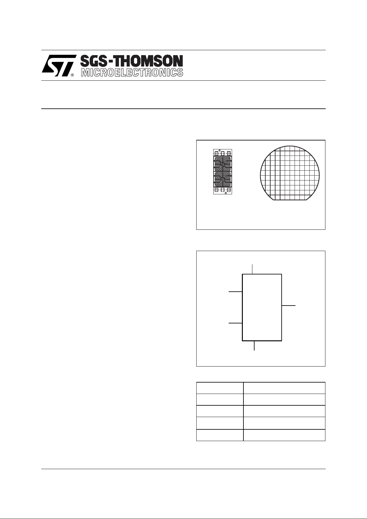
Figure 1. Del iv ery Forms
Micromodule Wafer
Figure 2. Pin Co nn e ct i on
V
CC
RST
ST1305
CLK
GND
Table 1. Signal Names
CLK Clock
RST Reset
I/O Serial Data Input/Output
V
CC
GND Ground
Supply Voltage
I/O
AI01032
1/2BD.05/9803V1

ST1305
The device offers two distinct configurations:
– ISSUER: for the card manufacturer, allowing special data to be written to the chip, during initialisation
– USER: for the end user of the card, restricting access to the chip.
Before delivery, from ST to the card issuer, the device is placed in the ISS UE R c onfigurat ion. Th is oper-
ation is performed by blowing the “test fuse”.
Figure 3. Me m ory Map
In USER Configuration
000d
016d
064d
Circuit Identification
Card Identification
16 bits
48 bits
EEPROM
Cells
Matrix
READ
ONLY
Counters / Transport Code
112d
Certificate / Transport Code
128d
Issuer Defined Area
192d
260d
Unused
Fuses
48 bits
16 bits
64 bits
READ, WRITE,
ERASE
READ
ONLY
DS0502
ORDERING INFORMATION SCHEME
For a full list of the available options, please see the current Memory Shortform Catalogue.
For further information on any aspect of this device, please contact your nearest ST Sales Office.
Example:
ST1305 - W2 / XX YY
DS0501
2/2
Delivery Form
U: Micromodule on reel
W2: Wafer 280 µm thickness
Customer Code
Transport Code
Given by ST
 Loading...