

Page 1
GENERAL DESCRIPTION
ST16C450
UNIVERSAL ASYNCHRONOUS
RECEIVER/TRANSMITTER (UART)
September 2003
The ST16C450 is a universal asynchronous receiver
and transmitter. The ST16C450 is an improved version of the NS16450 UART with higher operating
speed and lower access time. A programmable baud
rate generator is provided to select transmit and
receive clock rates from 50 Bps to 1.5 Mbps.
The ST16C450 on board status registers provides the
error conditions, type and status of the transfer
operation being performed. Included is complete
MODEM control capability, and a processor interrupt
system that may be software tailored to the user’s
requirements. The ST16C450 provides internal loopback capability for on board diagnostic testing.
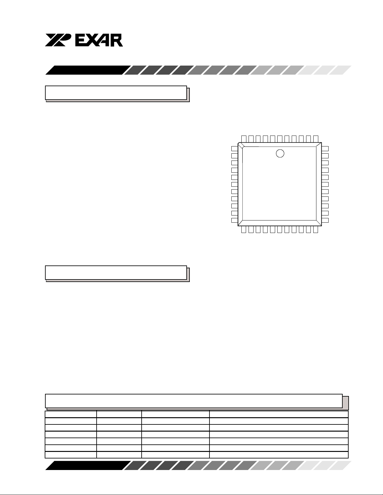
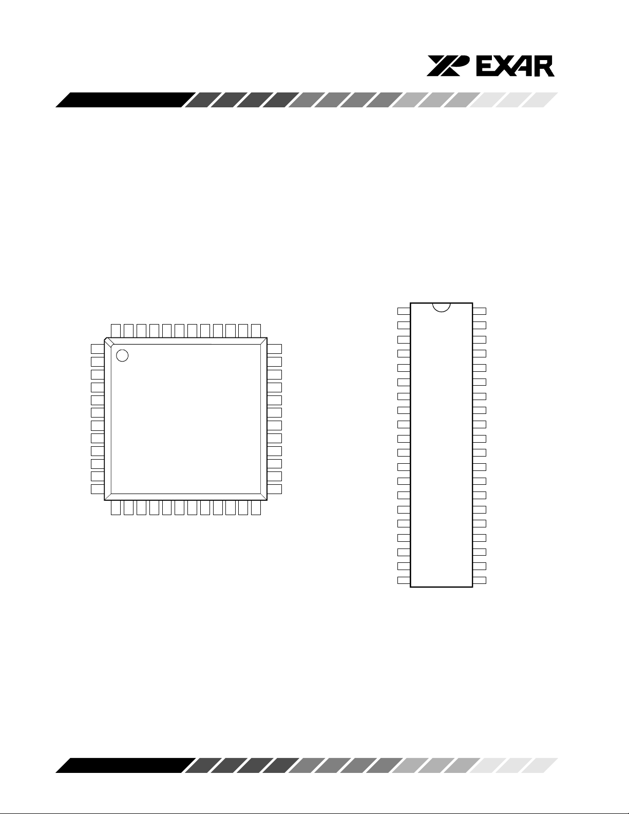
The ST16C450 is available in 40 pin PDIP, 44 pin
PLCC, and 48 pin TQFP packages. It is fabricated in
an advanced CMOS process to achieve low drain
power and high speed requirements.
FEATURES
RCLK
N.C.
CS0
CS1
-CS2
-BAUDOUT
PLCC Package
D4D3D2D1D0
6
5
4
7
D5
8
D6
9
D7
10
11
RX
12
13
TX
14
15
16
17
1819202122232425262728
-IOW
XTAL1
XTAL2
N.C.
VCC
321
ST16C450CJ44
IOW
N.C.
GND
4443424140
-IOR
-RI
IOR
-CD
-DSR
-CTS
39
RESET
38
-OP1
37
-DTR
36
-RTS
35
-OP2
34
N.C.
33
INT
32
N.C.
31
A0
30
A1
29
A2
-AS
-DDIS
CSOUT
• Pin to pin and functionally compatible to the Industry Standard 16450
• 2.97 to 5.5 volt operation
• 1.5 Mbps transmit/receive operation (24MHz)
• Programmable word lengths (5, 6, 7, 8)
• Even, odd, force, or no parity generation and
detection
• Independent transmit and receive control
• Standard modem interface
• Low operating current ( 1.2mA typ.)
ORDERING INFORMATION
Part number Package Operating temperature Device Status
ST16C450CP40 40-Lead PDIP 0° C to + 70° C Active. See the ST16C450CQ48 for new designs.
ST16C450CJ44 44-Lead PLCC 0° C to + 70° C Active
ST16C450CQ48 48-Lead TQFP 0° C to + 70° C Active
ST16C450IP40 40-Lead PDIP -40° C to + 85° C Active. See the ST16C450IQ48 for new designs.
ST16C450IJ44 44-Lead PLCC -40° C to + 85° C Active
ST16C450IQ48 48-Lead TQFP -40° C to + 85° C Active
Rev. 4.20
EXAR Corporation, 48720 Kato Road, Fremont, CA 94538 • (510) 668-7000 • FAX (510) 668-7017
Page 2
ST16C450
48 Pin TQFP Package 40 Pin DIP Package
Figure 1, PACKAGE DESCRIPTION, ST16C450
N.C.
RCLK
N.C.
CS0
CS1
-CS2
-BAUDOUT
1
N.C.
D4D3D2D1D0
4847464544434241403938
1
2
D5
3
D6
4
D7
5
6
7
RX
8
TX
9
10
11
12
1314151617181920212223
N.C.
XTAL1
XTAL2
ST16C450CQ48
-IOW
VCC
-RI
-CD
-DSR
-CTS
N.C.
37
N.C.
36
RESET
35
-OP1
34
-DTR
33
-RTS
32
-OP2
31
INT
30
N.C.
29
A0
28
A1
27
A2
26
N.C.
25
24
N.C.
IOR
-IOR
GND
IOW
-AS
-DDIS
CSOUT
D0
D1
D2
D3
D4
D5
D6
D7
RCLK
RX
TX
CS0
CS1
-CS2
-BAUDOUT
XTAL1
XTAL2
-IOW
IOW
GND
2
3
4
5
6
7
8
9
10
11
12
ST16C450CP40
13
14
15
16
17
18
19
20
VCC
40
-RI
39
-CD
38
-DSR
37
-CTS
36
RESET
35
-OP1
34
-DTR
33
-RTS
32
-OP2
31
INT
30
N.C.
29
A0
28
A1
27
A2
26
-AS
25
CSOUT
24
-DDIS
23
IOR
22
-IOR
21
Rev. 4.20
2
Page 3
D0-D7
-IOR,IOR
-IOW,IOW
RESET
ST16C450
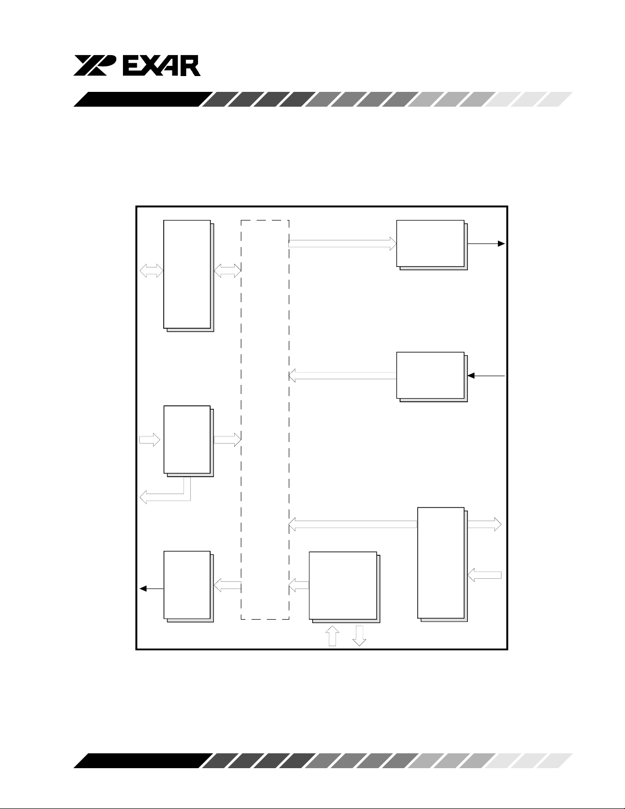
Figure 2, BLOCK DIAGRAM
Transmit
Shift
Register
&
Data bus
Control Logic
Receive
Shift
Register
TX
RX
A0-A2
-AS
CS0,CS1
-CS2
-DDIS
CSOUT
INT
Register
Interrupt
Select
Control
Logic
Logic
&
Control signals
Inter Connec t Bus Lines
-DTR,-RTS
-OP1,-OP2
Clock
&
Baud Rate
Generator
RCLK
XTAL1
Modem
Control
Logic
XTAL2
-BAUDOUT
-CTS
-RI
-CD
-DSR
Rev. 4.20
3
Page 4
ST16C450
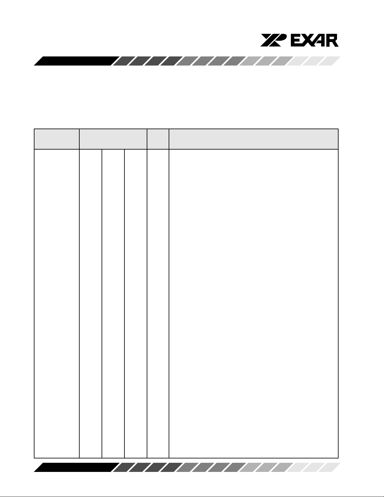
SYMBOL DESCRIPTION
Symbol Pin Signal Pin Description
40 44 48 type
A0 2 8 3 1 2 8 I Address-0 Select Bit Internal registers address selection.
A1 27 30 27 I Address-1 Select Bit Internal registers address selection.
A2 26 29 26 I Address-2 Select Bit Internal registers address selection.
IOR 22 25 20 I Read data strobe. Its function is the same as -IOR (see -
IOR), except it is active high. Either an active -IOR or IOR
is required to transfer data from 16C450 to CPU during a
read operation.
CS0 12 14 9 I Chip Select-0. Logical 1 on this pin provides the chip select-
0 function.
CS1 13 15 10 I Chip Select-1. Logical 1 on this pin provides the chip select-
1 function.
-CS2 14 16 11 I Chip Select -2. Logical 0 on this pin provides the chip select2 function.
IO W 19 21 17 I Write data strobe. Its function is the same as -IOW (see -
IOW), but it acts as an active high input signal. Either -IOW
or IOW is required to transfer data from the CPU to
ST16C450 during a write operation.
-AS 25 28 24 I Address Strobe. A logic 0 transition on -AS latches the state
of the chip selects and the register select bits, A0-A2. This
input is used when address and chip selects are not stable
for the duration of a read or write operation, i.e., a microprocessor that needs to de-multiplex the address and data bits.
If not required, the -AS input can be permanently tied to a
logic 0 (it is edge triggered).
D0-D7 1-8 2-9 43-47
2-4 I/ O Data Bus (Bi-directional) - These pins are the eight bit, tri-
state data bus for transferring information to or from the
controlling CPU. D0 is the least significant bit and the first
data bit in a transmit or receive serial data stream.
GN D 2 0 22 18 Pw r Signal and Power Ground.
Rev. 4.20
4
Page 5
ST16C450
SYMBOL DESCRIPTION
Symbol Pin Signal Pin Description
40 44 48 type
-IOR 21 24 19 I Read data strobe (active low strobe). A logic 0 on this pin
transfers the contents of the ST16C450 data bus to the
CPU.
-IOW 18 20 16 I Write data strobe (active low strobe). A logic 0 on this pin
transfers the contents of the CPU data bus to the addressed
internal register.
INT 30 33 30 O Interrupt Request (active high). Interrupts are enabled in the
interrupt enable register (IER), and when an interrupt condition exists. Interrupt conditions include: receiver errors,
available receiver buffer data, transmit buffer empty, or
when a modem status flag is detected.
CSOUT 24 27 23 O Chip select out. A high on this pin indicates that the
ST16C450 has been enabled by the chip select pin.
-BAUDOUT 15 17 12 O Baud Rate Generator Output. This pin provides the 16X
clock of the selected data rate from the baud rate generator.
The RCLK pin must be connected externally to -BAUDOUT
when the receiver is operating at the same data rate.
-DDIS 23 26 22 O Drive Disable. This pin goes to a logic 0 when the external
CPU is reading data from the ST16C450. This signal can be
used to disable external transceivers or other logic functions.
-OP1 34 38 34 O Output-1 (User Defined) - See bit-2 of modem control
register (MCR bit-2).
RESET 35 39 35 I Reset. (active high) - A logic 1 on this pin will reset the
internal registers and all the outputs. The UART transmitter
output and the receiver input will be disabled during reset
time. (See ST16C450 External Reset Conditions for initialization details.)
RCLK 9 10 5 I Receive Clock Input. This pin is used as external 16X clock
input to the receiver section. External connection to Baudout pin is required in order to utilize the internal baud
rate generator.
Rev. 4.20
5
Page 6
ST16C450
SYMBOL DESCRIPTION
Symbol Pin Signal Pin Description
40 44 48 type
-OP2 31 35 31 O Output-2 (User Defined). This pin provides the user a general
purpose output. See bit-3 modem control register (MCR bit-
3).
VCC 40 44 42 Pwr Power Supply Input.
XTAL1 16 18 14 I Crystal or External Clock Input - Functions as a crystal input
or as an external clock input. A crystal can be connected
between this pin and XTAL2 to form an internal oscillator
circuit. An external 1 MW resistor is required between the
XTAL1 and XTAL2 pins (see figure 3). Alternatively, an
external clock can be connected to this pin to provide
custom data rates (Programming Baud Rate Generator
section).
XTAL2 17 19 15 O Output of the Crystal Oscillator or Buffered Clock - (See also
XTAL1). Crystal oscillator output or buffered clock output.
-CD 38 42 40 I Carrier Detect (active low) - A logic 0 on this pin indicates
that a carrier has been detected by the modem.
-CTS 36 40 38 I Clear to Send (active low) - A logic 0 on the -CTS pin
indicates the modem or data set is ready to accept transmit
data from the ST16C450. Status can be tested by reading
MSR bit-4. This pin has no effect on the UART’s transmit or
receive operation.
-DSR 37 41 39 I Data Set Ready (active low) - A logic 0 on this pin indicates
the modem or data set is powered-on and is ready for data
exchange with the UART. This pin has no effect on the
UART’s transmit or receive operation.
-DTR 33 37 33 O Data Terminal Ready (active low) - A logic 0 on this pin
indicates that the ST16C450 is powered-on and ready. This
pin can be controlled via the modem control register.
Writing a logic 1 to MCR bit-0 will set the -DTR output to
logic 0, enabling the modem. This pin will be a logic 1 after
writing a logic 0 to MCR bit-0, or after a reset. This pin has
no effect on the UART’s transmit or receive operation.
Rev. 4.20
6
Page 7
ST16C450
SYMBOL DESCRIPTION
Symbol Pin Signal Pin Description
40 44 48 type
-R I 39 43 41 I Ring Indicator (active low) - A logic 0 on this pin indicates the
modem has received a ringing signal from the telephone
line. A logic 1 transition on this input pin will generate an
interrupt.
-RTS 32 36 32 O Request to Send (active low) - A logic 0 on the -RTS pin
indicates the transmitter has data ready and waiting to send.
Writing a logic 1 in the modem control register (MCR bit-1)
will set this pin to a logic 0 indicating data is available. After
a reset this pin will be set to a logic 1. This pin has no effect
on the UART’s transmit or receive operation.
RX 10 11 7 I Receive Data - This pin provides the serial receive data
input to the ST16C450. The RX signal will be a logic 1 during
reset, idle (no data). During the local loop-back mode, the
RX input pin is disabled and TX data is internally connected
to the UART RX Input, internally, see figure 12.
TX 11 13 8 O Transmit Data - This pin provides the serial transmit data
from the ST16C450, the TX signal will be a logic 1 during
reset, idle (no data). During the local loop-back mode, the
TX input pin is disabled and TX data is internally connected
to the UART RX Input, see figure 12.
GENERAL DESCRIPTION
provide all these functions is fairly complex especially
The ST16C450 provides serial asynchronous receive
data synchronization, parallel-to-serial and serial-toparallel data conversions for both the transmitter and
receiver sections. These functions are necessary for
converting the serial data stream into parallel data that
is required with digital data systems. Synchronization
for the serial data stream is accomplished by adding
start and stops bits to the transmit data to form a data
character (character orientated protocol). Data integrity is insured by attaching a parity bit to the data
character. The parity bit is checked by the receiver for
any transmission bit errors. The electronic circuitry to
when manufactured on a single integrated silicon chip.
The ST16C450 represents such an integration with
greatly enhanced features. The ST16C450 is fabricated
with an advanced CMOS process. The ST16C450 is
designed to work with high speed modems and shared
network environments.
The ST16C450 is capable of operation to 1.5Mbps
with a 24 MHz crystal or external clock input.
With a crystal of 14.7464 MHz and through a software
option, the user can select data rates up to 460.8Kbps
or 921.6Kbps.
Rev. 4.20
7
Page 8
ST16C450
FUNCTIONAL DESCRIPTIONS
Internal Registers
The ST16C450 provides 11 internal registers for
monitoring and control. These registers are shown in
Table 2 below. These registers function as data holding
registers (THR/RHR), interrupt status and control
registers (IER/ISR), line status and control registers,
(LCR/LSR), modem status and control registers (MCR/
MSR), programmable data rate (clock) control registers
(DLL/DLM), and a user assessable scratchpad register
(SPR).
Table 2, INTERNAL REGISTER DECODE
A2 A1 A0 READ MODE WRITE MODE
General Register Set (THR/RHR, IER/ISR, MCR/MSR, LCR/LSR, SPR):
0 0 0 Receive Holding Register Transmit Holding Register
0 0 1 Interrupt Enable Register
0 1 0 Interrupt Status Register
0 1 1 Line Control Register
1 0 0 Modem Control Register
1 0 1 Line Status Register
1 1 0 Modem Status Register
1 1 1 Scratchpad Register Scratchpad Register
Baud Rate Register Set (DLL/DLM): Note *3
0 0 0 LSB of Divisor Latch LSB of Divisor Latch
0 0 1 MSB of Divisor Latch MSB of Divisor Latch
Note *3: These registers are accessible only when LCR bit-7 is set to a logic 1.
Rev. 4.20
8
Page 9
ST16C450
Programmable Baud Rate Generator
The ST16C450 supports high speed modem technologies that have increased input data rates by
employing data compression schemes. For example
a 33.6Kbps modem that employs data compression
may require a 115.2Kbps input data rate. A 128.0Kbps
ISDN modem that supports data compression may
need an input data rate of 460.8Kbps. The ST16C450
can support a standard data rate of 921.6Kbps.
The programmable Baud Rate Generator is capable of
accepting an input clock up to 24 MHz, as required for
supporting a 1.5Mbps data rate. The ST16C450 can be
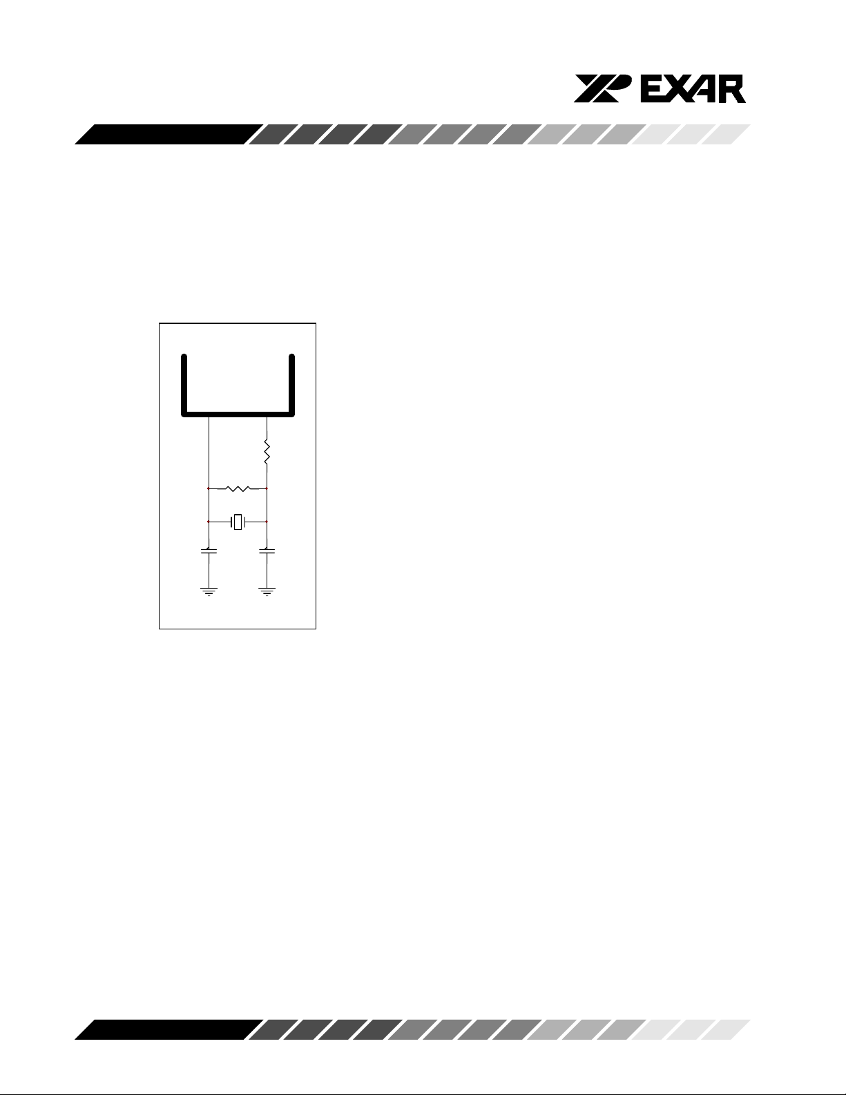
configured for internal or external clock operation. For
internal clock oscillator operation, an industry standard
microprocessor crystal (parallel resonant/ 22-33 pF
load) is connected externally between the XTAL1 and
XTAL2 pins, with an external 1 MΩ resistor across it.
Table 3, BAUD RATE GENERATOR PROGRAMMING TABLE (1.8432 MHz CLOCK):
Alternatively, an external clock can be connected to the
XTAL1 pin to clock the internal baud rate generator for
standard or custom rates. See figure 3 for crystal
oscillator connection.
The generator divides the input 16X clock by any
divisor from 1 to 216 -1. The ST16C450 divides the
basic crystal or external clock by 16. The frequency of
the -BAUDOUT output pin is exactly 16X (16 times) of
the selected baud rate (-BAUDOUT =16 x Baud Rate).
Customized Baud Rates can be achieved by selecting
the proper divisor values for the MSB and LSB sections
of baud rate generator.
Programming the Baud Rate Generator Registers DLM
(MSB) and DLL (LSB) provides a user capability for
selecting the desired final baud rate. The example in
Table 3 below.
Output User User DLM DLL
Baud Rate 16 x Clock 16 x Clock Program Program
Divisor Divisor Value Value
(Decimal) (HEX) (HEX) (HEX)
50 2304 900 09 00
75 1536 600 06 00
150 768 300 03 00
300 384 180 01 80
600 192 C0 00 C0
1200 96 60 00 60
2400 48 30 00 30
4800 24 18 00 18
7200 16 10 00 10
9600 12 0C 00 0C
19.2k 6 06 00 06
38.4k 3 03 00 03
57.6k 2 02 00 02
115.2k 1 01 00 01
Rev. 4.20
9
Page 10
ST16C450
Figure 3, EXTERNAL CRYSTAL OSCILLATOR
CONNECTION
XTAL1
C1
22pF
R2
1M
X1
1.8432 MHz
XTAL2
R1
50-120
C2
33pF
associated interface pins, and instead are connected
together internally (See Figure 4). The -CTS, -DSR, -CD,
and -RI are disconnected from their normal modem
control inputs pins, and instead are connected internally to -DTR, -RTS, -OP1 and -OP2. Loop-back test
data is entered into the transmit holding register via the
user data bus interface, D0-D7. The transmit UART
serializes the data and passes the serial data to the
receive UART via the internal loop-back connection. The
receive UART converts the serial data back into parallel
data that is then made available at the user data
interface, D0-D7. The user optionally compares the
received data to the initial transmitted data for verifying
error free operation of the UART TX/RX circuits.
In this mode , the receiver and transmitter interrupts are
fully operational. The Modem Control Interrupts are also
operational. However, the interrupts can only be read
using lower four bits of the Modem Control Register
(MCR bits 0-3) instead of the four Modem Status
Register bits 4-7. The interrupts are still controlled by
the IER.
Loopback Mode
The internal loop-back capability allows onboard diagnostics. In the loop-back mode the normal modem
interface pins are disconnected and reconfigured for
loop-back internally. In this mode MSR bits 4-7 are
also disconnected. However, MCR register bits 0-3
can be used for controlling loop-back diagnostic testing. In the loop-back mode -OP1 and -OP2 in the MCR
register (bits 0-1) control the modem -RI and -CD
inputs respectively. MCR signals -DTR and -RTS (bits
0-1) are used to control the modem -CTS and -DSR
inputs respectively. The transmitter output (TX) and
the receiver input (RX) are disconnected from their
Rev. 4.20
10
Page 11
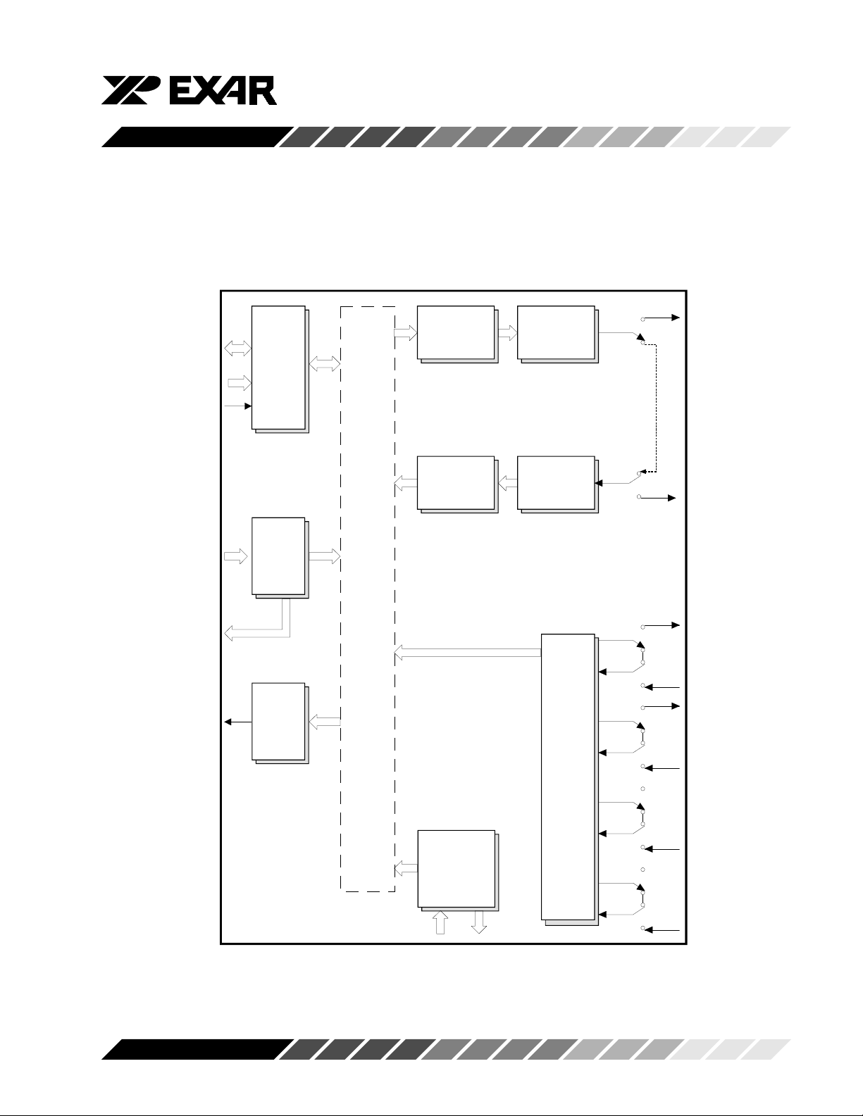
Figure 4, INTERNAL LOOPBACK MODE DIAGRAM
ST16C450
D0-D7
-IOR,IOR
-IOW,I OW
RESET
A0-A2
-AS
CS0,CS1
-CS2
-DDIS
CSOUT
INT
Transmit
Holding
Registers
&
Data bus
Control Logic
Receive
Holding
Registers
Logic
Select
Register
&
C on trol signals
Inter C o nn ect B u s L ines
Logic
Control
Interrupt
Transmit
Shift
Register
Receive
Shift
Register
TX
MCR Bit-4=1
RX
-RTS
-CD
-DTR
Rev. 4.20
Clock
&
Baud Rate
Generator
RCLK
XTAL1
11
-RI
-OP1
Modem Control Logic
-DSR
-OP2
-CTS
XTAL2
-BAUDOUT
Page 12
ST16C450
REGISTER FUNCTIONAL DESCRIPTIONS
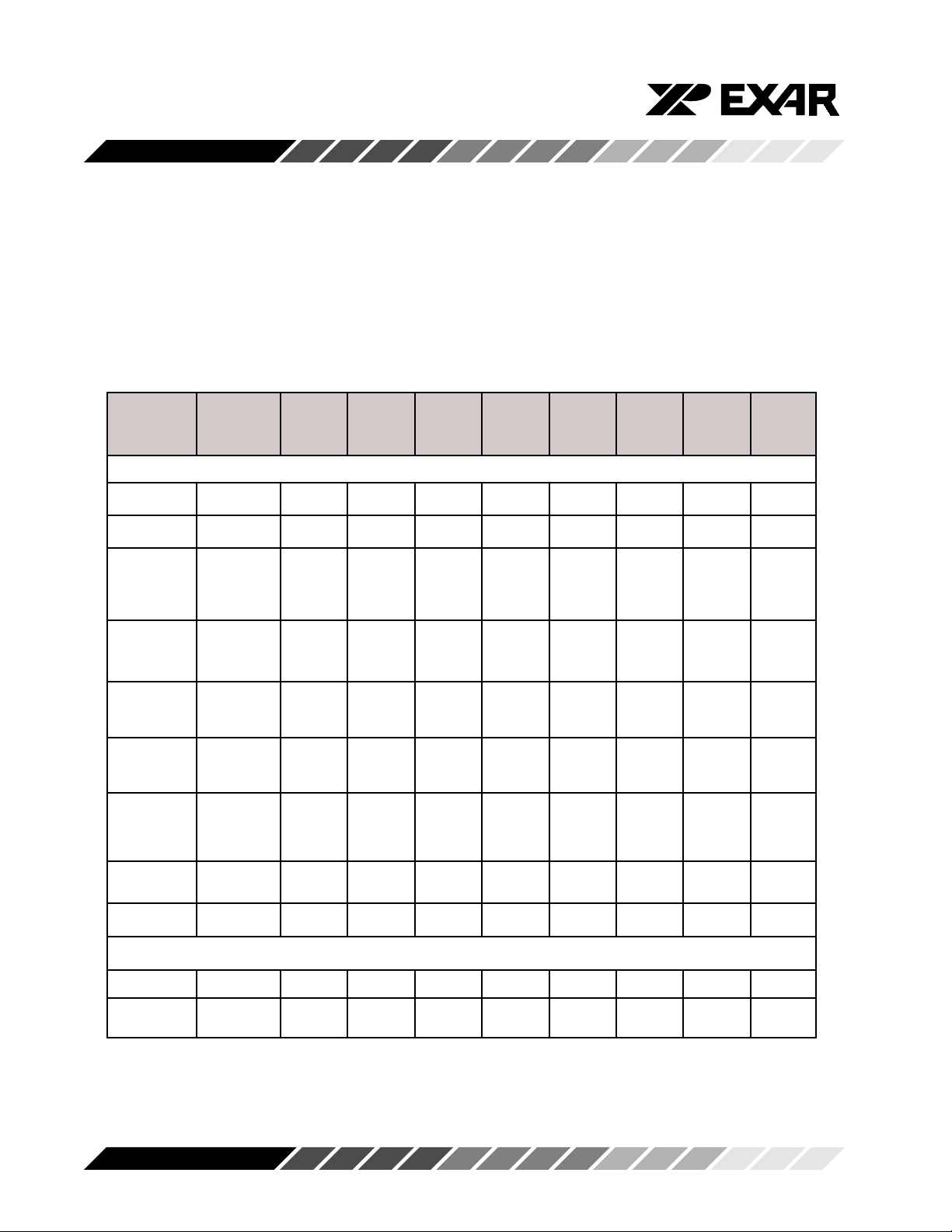
The following table delineates the assigned bit functions for the twelve ST16C450 internal registers. The assigned bit functions are more fully defined in the following paragraphs.
Table 4, ST16C450 INTERNAL REGISTERS
A2 A1 A0 Register BIT-7 BIT-6 BIT-5 BIT-4 BIT-3 BIT-2 BIT-1 BIT-0
[Default]
Note *5
General Register Set
0 0 0 RHR [XX] bit-7 bit-6 bit-5 bit-4 bit-3 bit-2 bit-1 bit-0
0 0 0 THR [XX] bit-7 bit-6 bit-5 bit-4 bit-3 bit-2 bit-1 bit-0
0 0 1 IER [00] 0000modem receive transmit receive
0 1 0 ISR [01] 0000INTINTINTINT
0 1 1 LCR [00] divisor set set even parity stop word word
latch break parity parity enable bits length length
enable bit-1 bit-0
1 0 0 MCR [00] 0 0 0 loop -OP2 -OP1 -RTS -DTR
back
1 0 1 LSR [60] 0 trans. trans. break framing parity overrun receive
empty holding interrupt error error error data
empty ready
status line holding holding
interrupt status register register
interrupt
priority priority priority status
bit-2 bit-1 bit-0
1 1 0 MSR [X0] CD RI DSR CTS delta delta delta delta
1 1 1 SPR [FF] bit-7 bit-6 bit-5 bit-4 bit-3 bit-2 bit-1 bit-0
-CD -RI -DSR -CTS
Special Register Set: Note *3
0 0 0 DLL [XX] bit-7 bit-6 bit-5 bit-4 bit-3 bit-2 bit-1 bit-0
0 0 1 DLM [XX] bit-15 bit-14 bit-13 bit-12 bit-11 bit-10 bit-9 bit-8
Note *3: The Special register set is accessible only when LCR bit-7 is set to a logic 1.
Note *5: The value represents the register’s initialized HEX value. An “X” signifies a 4-bit un-initialized nibble.
Rev. 4.20
12
Page 13

ST16C450
Transmit and Receive Holding Register
The serial transmitter section consists of an 8-bit
Transmit Hold Register (THR) and Transmit Shift
Register (TSR). The status of the THR is provided in
the Line Status Register (LSR). Writing to the THR
transfers the contents of the data bus (D7-D0) to the
THR, providing that the THR or TSR is empty. The
THR empty flag in the LSR register will be set to a logic
1 when the transmitter is empty or when data is
transferred to the TSR. Note that a write operation can
be performed when the transmit holding register
empty flag is set.
The serial receive section also contains an 8-bit
Receive Holding Register, RHR. Receive data is
removed from the ST16C450 and receive by reading
the RHR register. The receive section provides a
mechanism to prevent false starts. On the falling edge
of a start or false start bit, an internal receiver counter
starts counting clocks at 16x clock rate. After 7 1/2
clocks the start bit time should be shifted to the center
of the start bit. At this time the start bit is sampled and
if it is still a logic 0 it is validated. Evaluating the start
bit in this manner prevents the receiver from assembling a false character. Receiver status codes will be
posted in the LSR.
Interrupt Enable Register (IER)
IER BIT-2:
Logic 0 = Disable the receiver line status interrupt.
(normal default condition)
Logic 1 = Enable the receiver line status interrupt.
IER BIT-3:
Logic 0 = Disable the modem status register interrupt.
(normal default condition)
Logic 1 = Enable the modem status register interrupt.
IER BIT 4-7:
Interrupt Status Register (ISR)
The ST16C450 provides four levels of prioritized
interrupts to minimize external software interaction.
The Interrupt Status Register (ISR) provides the user
with four interrupt status bits. Performing a read cycle
on the ISR will provide the user with the highest
pending interrupt level to be serviced. No other interrupts are acknowledged until the pending interrupt is
serviced. Whenever the interrupt status register is
read, the interrupt status is cleared. However it should
be noted that only the current pending interrupt is
cleared by the read. A lower level interrupt may be seen
after rereading the interrupt status bits. The Interrupt
Source Table 5 (below) shows the data values (bit 0-3)
for the four prioritized interrupt levels and the interrupt
sources associated with each of these interrupt levels:
Not used and set to “0”.
The Interrupt Enable Register (IER) masks the interrupts from receiver ready, transmitter empty, line
status and modem status registers. These interrupts
would normally be seen on the ST16C450 INT output
pin.
IER BIT-0:
Logic 0 = Disable the receiver ready interrupt. (normal
default condition)
Logic 1 = Enable the receiver ready interrupt.
IER BIT-1:
Logic 0 = Disable the transmitter empty interrupt.
(normal default condition)
Logic 1 = Enable the transmitter empty interrupt.
Rev. 4.20
13
Page 14
ST16C450
Table 5, INTERRUPT SOURCE TABLE
Priority [ISR]
Level B it-3 Bit-2Bit-1 Bit-0 Source of the interrupt
1 0 1 1 0 LSR (Receiver Line Status Register)
2 0 1 0 0 RXRDY (Received Data Ready)
3 0 0 1 0 TXRDY ( Transmitter Holding Register Empty)
4 0 0 0 0 MSR (Modem Status Register)
ISR BIT-0:
Logic 0 = An interrupt is pending and the ISR contents
may be used as a pointer to the appropriate interrupt
service routine.
Logic 1 = No interrupt pending. (normal default condition)
ISR BIT 1-3: (logic 0 or cleared is the default condition)
These bits indicate the source for a pending interrupt
at interrupt priority levels 1, 2, and 3 (See Interrupt
Source Table).
ISR BIT 4-7
Line Control Register (LCR)
The Line Control Register is used to specify the
asynchronous data communication format. The word
length, the number of stop bits, and the parity are
selected by writing the appropriate bits in this register.
LCR BIT 0-1: (logic 0 or cleared is the default condition)
These two bits specify the word length to be transmitted or received.
BIT-1 BIT-0 Word length
00 5
01 6
10 7
11 8
: Not used and set to “0”.
LCR BIT-2: (logic 0 or cleared is the default condition)
The length of stop bit is specified by this bit in conjunction with the programmed word length.
BIT-2 Word length Stop bit
length
(Bit time(s))
0 5,6,7,8 1
1 5 1-1/2
1 6,7,8 2
LCR BIT-3:
Parity or no parity can be selected via this bit.
Logic 0 = No parity (normal default condition)
Logic 1 = A parity bit is generated during the transmission, receiver checks the data and parity for transmission errors.
LCR BIT-4:
If the parity bit is enabled with LCR bit-3 set to a logic
1, LCR BIT-4 selects the even or odd parity format.
Logic 0 = ODD Parity is generated by forcing an odd
number of logic 1’s in the transmitted data. The
receiver must be programmed to check the same
format. (normal default condition)
Logic 1 = EVEN Parity is generated by forcing an even
the number of logic 1’s in the transmitted. The receiver
must be programmed to check the same format.
LCR BIT-5:
If the parity bit is enabled, LCR BIT-5 selects the
forced parity format.
Rev. 4.20
14
Page 15
ST16C450
LCR BIT-5 = logic 0, parity is not forced (normal default
condition)
LCR BIT-5 = logic 1 and LCR BIT-4 = logic 0, parity bit
is forced to a logical 1 for the transmit and receive
data.
LCR BIT-5 = logic 1 and LCR BIT-4 = logic 1, parity bit
is forced to a logical 0 for the transmit and receive
data.
LCR LCR LCR Parity selection
Bit-5 Bit-4 Bit-3
X X 0 No parity
0 0 1 Odd parity
0 1 1 Even parity
1 0 1 Force parity”1”
1 1 1 Forced parity “0”
LCR BIT-6:
When enabled the Break control bit causes a break
condition to be transmitted (the TX output is forced to
a logic 0 state). This condition exists until disabled by
setting LCR bit-6 to a logic 0.
Logic 0 = No TX break condition. (normal default
condition)
Logic 1 = Forces the transmitter output (TX) to a logic
0 for alerting the remote receiver to a line break
condition.
LCR BIT-7:
The internal baud rate counter latch and Enhance
Feature mode enable.
Logic 0 = Divisor latch disabled. (normal default
condition)
Logic 1 = Divisor latch and enhanced feature register
enabled.
Modem Control Register (MCR)
This register controls the interface with the modem or a
peripheral device.
MCR BIT-0:
Logic 0 = Force -DTR output to a logic 1. (normal
default condition)
Logic 1 = Force -DTR output to a logic 0.
MCR BIT-1:
Logic 0 = Force -RTS output to a logic 1. (normal default
condition)
Logic 1 = Force -RTS output to a logic 0.
MCR BIT-2:
Logic 0 = Set -OP1 output to a logic 1. (normal default
condition)
Logic 1 = Set -OP1 output to a logic 0.
MCR BIT-3:
Logic 0 = Set -OP2 output to a logic 1. (normal default
condition)
Logic 1 = Set -OP2 output to a logic 0.
MCR BIT-4:
Logic 0 = Disable loop-back mode. (normal default
condition)
Logic 1 = Enable local loop-back mode (diagnostics).
MCR BIT 5-7:
Line Status Register (LSR)
This register provides the status of data transfers
between. the ST16C450 and the CPU.
Not used and set to “0”.
LSR BIT-0:
Logic 0 = No data in receive holding register. (normal
default condition)
Logic 1 = Data has been received and is saved in the
receive holding register.
LSR BIT-1:
Logic 0 = No overrun error. (normal default condition)
Logic 1 = Overrun error. A data overrun error occurred
in the receive shift register. This happens when additional data arrives while the RHR is full. In this case the
previous data in the shift register is overwritten. Note
that under this condition the data byte in the receive
shift register is not transfer into the RHR, therefore the
data in the RHR is not corrupted by the error.
LSR BIT-2:
Logic 0 = No parity error (normal default condition)
Logic 1 = Parity error. The receive character does not
have correct parity information and is suspect.
Rev. 4.20
15
Page 16

ST16C450
LSR BIT-3:
Logic 0 = No framing error (normal default condition).
Logic 1 = Framing error. The receive character did not
have a valid stop bit(s).
LSR BIT-4:
Logic 0 = No break condition (normal default condition)
Logic 1 = The receiver received a break signal.
LSR BIT-5:
This bit indicates that the ST16C450 is ready to accept
new characters for transmission. This bit causes the
ST16C450 to issue an interrupt to the CPU when the
transmit holding register is empty and the interrupt
enable is set.
Logic 0 = Transmit holding register is not empty.
(normal default condition)
Logic 1 = Transmit holding register is empty. When
this bit is a logic 1, the CPU can load a new characters
into the Transmit Holding Register for transmission.
LSR BIT-6:
Logic 0 = Transmitter holding and shift registers are
full.
Logic 1 = Transmitter holding and shift registers are
empty.
LSR BIT-7:
Modem Status Register (MSR)
This register provides the current state of the control
interface signals from the modem, or other peripheral
device that the ST16C450 is connected to. Four bits
of this register are used to indicate the changed
information. These bits are set to a logic 1 whenever
a control input from the modem changes state. These
bits are set to a logic 0 whenever the CPU reads this
register.
Not used and set to “0”.
MSR BIT-1:
Logic 0 = No -DSR Change (normal default condition)
Logic 1 = The -DSR input to the ST16C450 has
changed state since the last time it was read. A
modem Status Interrupt will be generated.
MSR BIT-2:
Logic 0 = No -RI Change (normal default condition)
Logic 1 = The -RI input to the ST16C450 has changed
from a logic 0 to a logic 1. A modem Status Interrupt
will be generated.
MSR BIT-3:
Logic 0 = No -CD Change (normal default condition)
Logic 1 = Indicates that the -CD input to the has
changed state since the last time it was read. A
modem Status Interrupt will be generated.
MSR BIT-4:
CTS (active high, logical 1). Normally this bit is the
compliment of the -CTS input. In the loop-back mode,
this bit is equivalent to the RTS bit in the MCR register.
MSR BIT-5:
DSR (active high, logical 1). Normally this bit is the
compliment of the -DSR input. In the loop-back mode,
this bit is equivalent to the DTR bit in the MCR register.
MSR BIT-6:
RI (active high, logical 1). Normally this bit is the
compliment of the -RI input. In the loop-back mode this
bit is equivalent to the OP1 bit in the MCR register.
MSR BIT-7:
CD (active high, logical 1). Normally this bit is the
compliment of the -CD input. In the loop-back mode
this bit is equivalent to the OP2 bit in the MCR register.
MSR BIT-0:
Logic 0 = No -CTS Change (normal default condition)
Logic 1 = The -CTS input to the ST16C450 has
changed state since the last time it was read. A
modem Status Interrupt will be generated.
Rev. 4.20
16
Page 17
Scratchpad Register (SPR)
The ST16C450 provides a temporary data register to
store 8 bits of user information.
ST16C450 EXTERNAL RESET CONDITIONS
REGISTERS RESET STATE
IER IER BITS 0-7 = logic 0
ISR ISR BIT-0=1, ISR BITS 1-7 = logic
0
LCR, MCR BITS 0-7 = logic 0
LSR LSR BITS 0-4 = logic 0,
LSR BITS 5-6 = logic 1 LSR, BIT
7 = logic 0
MSR MSR BITS 0-3 = logic 0,
MSR BITS 4-7 = logic levels of the
input signals
ST16C450
SIGNALS RESET STATE
TX Logic 1
-OP1 Logic 1
-OP2 Logic 1
-RTS Logic 1
-DTR Logic 1
CSOUT Logic 0
I N T Logic 0
Rev. 4.20
17
Page 18
ST16C450
AC ELECTRICAL CHARACTERISTICS
TA=0° - 70°C (-40° - +85°C for Industrial grade packages), Vcc=3.3 - 5.0 V ± 10% unless otherwise specified.
Symbol Parameter Limits Limits Units Conditions
3.3 5.0
Min Max Min Max
T1w,T2wClock pulse duration 1 7 17 ns
T
3w
T4w Address strobe width 35 2 5 ns
T5s Address setup time 5 0 ns
T5h Address hold time 5 5 ns
T
6s
T6h Chip select hold time 0 0 ns
T
7d
T
7w
T
7h
T
8d
T
9d
T
10d
T
11d
T
12d
T
12h
T
13d
T
13w
T
13h
T
14d
T
15d
T
16s
T
16h
T
17d
T
18d
T
19d
T
20d
T
21d
T
22d
T
23d
T
24d
T
R
N Baud rate devisor 1 216-1 1 216-1 Rclk
Oscillator/Clock frequency 8 2 4 MHz
Address setup time 5 0 ns
-IOR delay from chip select 10 10 ns Note 1:
-IOR strobe width 35 25 ns
Chip select hold time from -IOR 0 0 ns Note 1:
-IOR delay from address 10 10 ns Note 1:
Read cycle delay 40 30 ns
CSOUT delay from chip select 15 10 ns 100 pF load
-IOR to -DDIS delay 15 10 ns 100 pF load
Delay from -IOR to data 35 25 ns
Data disable time 25 15 ns
-IOW delay from chip select 10 10 ns Note 1:
-IOW strobe width 40 25 ns
Chip select hold time from -IOW 0 0 ns
-IOW delay from address 10 10 ns Note 1:
Write cycle delay 40 30 ns
Data setup time 20 15 ns
Data hold time 5 5 ns
Delay from -IOW to output 50 40 ns 100 pF load
Delay to set interrupt from MODEM 40 35 ns 100 pF load
input
Delay to reset interrupt from -IOR 40 35 ns 100 pF load
Delay from stop to set interrupt 1 1 Rclk
Delay from -IOR to reset interrupt 45 40 ns 100 pF load
Delay from stop to interrupt 45 40 ns
Delay from initial INT reset to transmit 8 24 8 24 Rclk
start
Delay from -IOW to reset interrupt 45 40 ns
Reset pulse width 40 40 ns
Note 1: Applicable only when -AS is tied low.
Rev. 4.20
18
Page 19
ST16C450
ABSOLUTE MAXIMUM RATINGS
Supply range 7 Volts
Voltage at any pin GND - 0.3 V to VCC +0.3 V
Operating temperature -40° C to +85° C
Storage temperature -65° C to 150° C
Package dissipation 500 mW
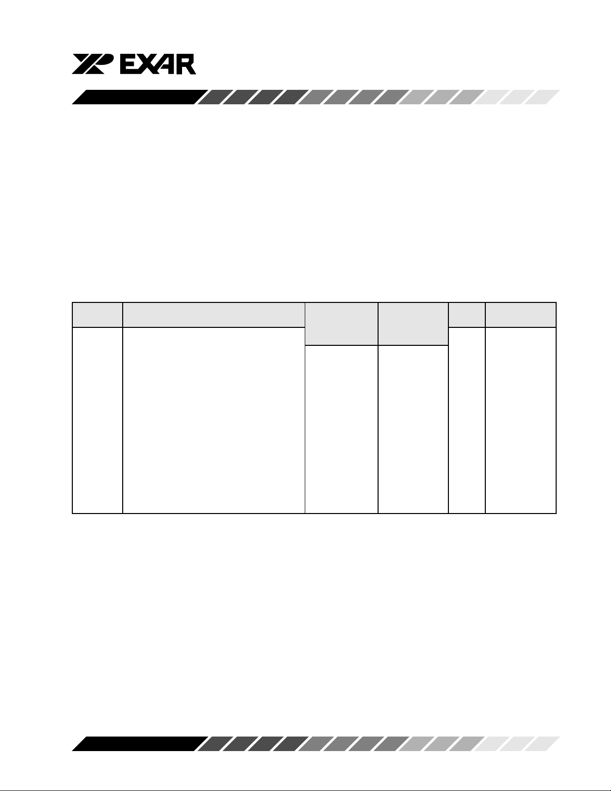
DC ELECTRICAL CHARACTERISTICS
TA=0° - 70°C (-40° - +85°C for Industrial grade packages), Vcc=3.3 - 5.0 V ± 10% unless otherwise specified.
Symbol Parameter Limits Limits Units Conditions
3.3 5.0
Min Max Min Max
V
ILCK
V
IHCK
V
IL
V
IH
V
OL
V
OL
V
OH
V
OH
I
IL
I
CL
I
CC
C
P
Clock input low level -0.3 0.6 -0.5 0.6 V
Clock input high level 2.4 VCC 3.0 VCC V
Input low level -0.3 0.8 -0.5 0.8 V
Input high level 2.0 2.2 VCC V
Output low level on all outputs 0.4 V IOL= 5 mA
Output low level on all outputs 0.4 V IOL= 4 mA
Output high level 2.4 V IOH= -5 mA
Output high level 2.0 V IOH= -1 mA
Input leakage ±10 ±10 µA
Clock leakage ±10 ±10 µA
Avg power supply current 1.3 3 mA
Input capacitance 5 5 pF
Rev. 4.20
19
Page 20
ST16C450
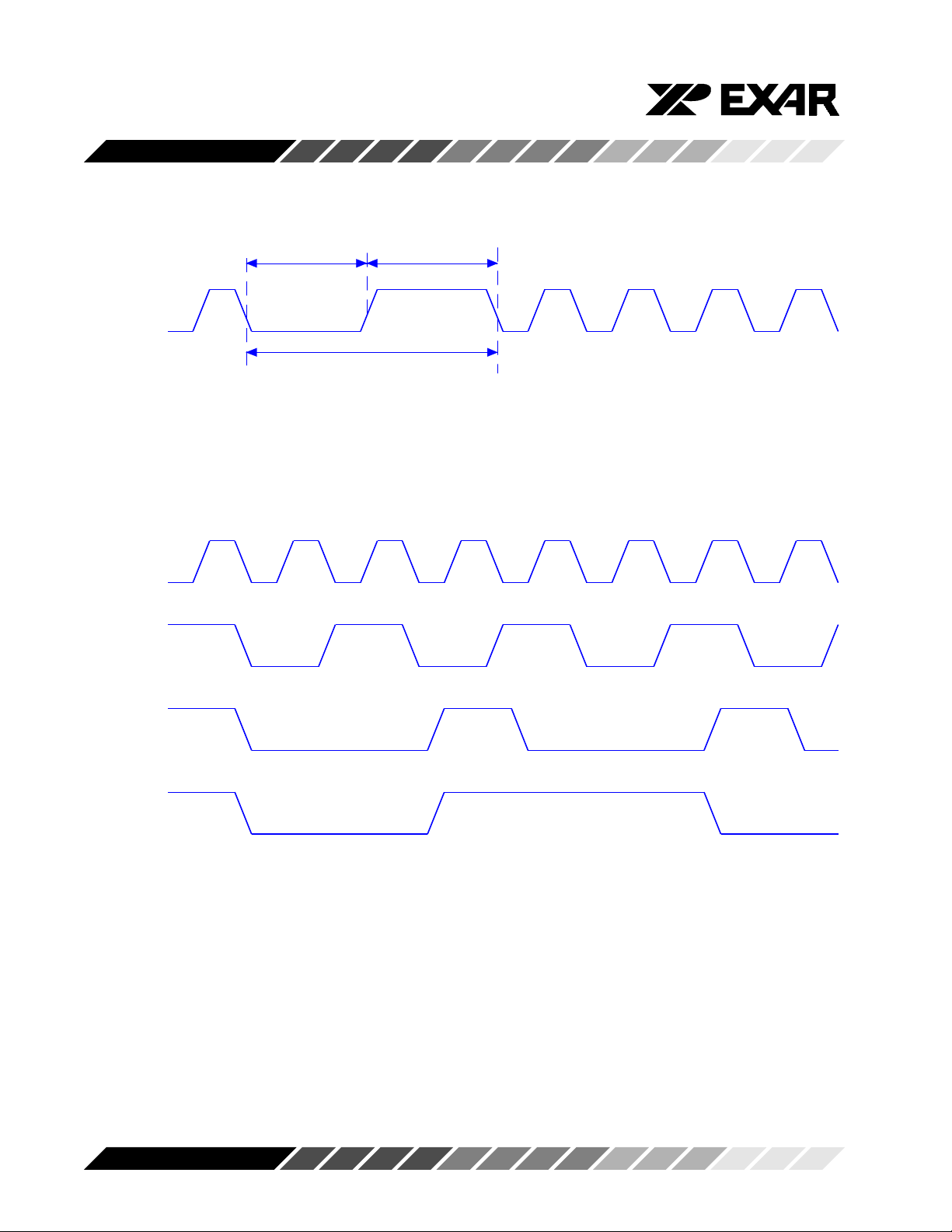
EXTERNAL
CLOCK
-BAUDOUT
1/2 -BAUDOUT
T2w
T1w
T3w
1/3 -BAUDOUT
1/3> -BAUDOUT
Rev. 4.20
X450-CK-1
Clock timing
20
Page 21
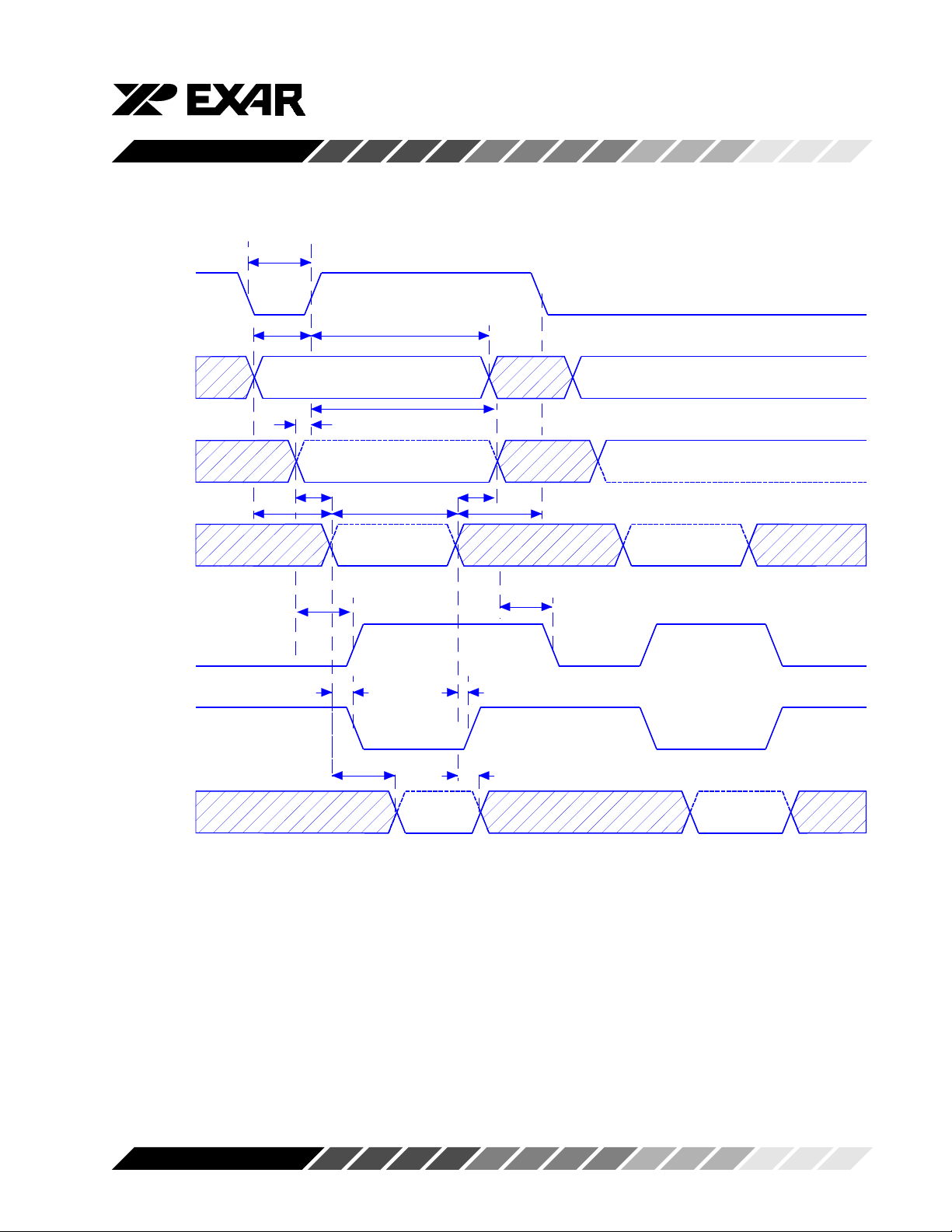
-AS
ST16C450
T4w
A0-A2
-CS2
CS1-CS0
-IOR
IOR
CSOUT
-DDIS
T8d
T5s
Valid
Address
T6s
Valid
T7d T7h
T10d
T11d
T12d
T7w
Active
Active
Active
T5h
T6h
T9d
T10d
T11d
T12h
D0-D7
Rev. 4.20
Data
X450-RD-1
General read timing
21
Page 22
ST16C450
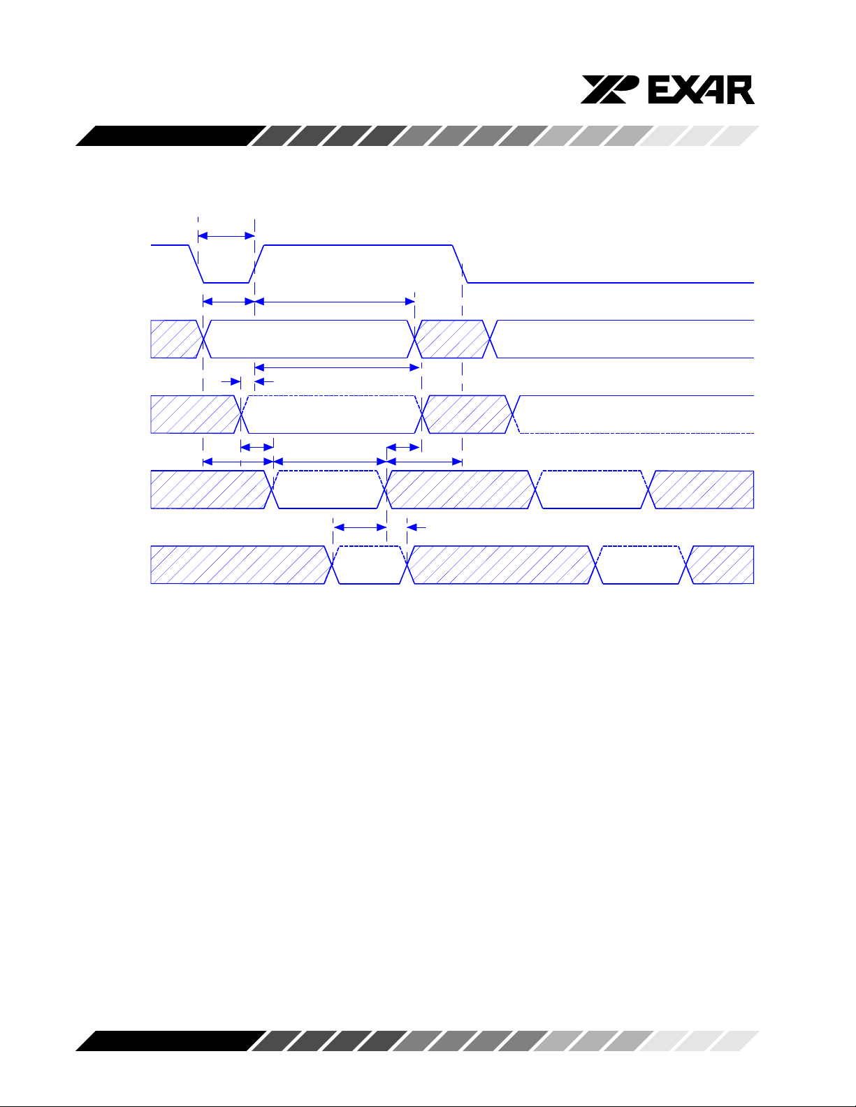
T4w
-AS
A0-A2
-CS2
CS1-CS0
-IOW
IOW
D0-D7
T5s
T14d
T5h
Valid
Address
T6s
Valid
T13d T13h
T13w
Active
T16s
Data
T6h
T16h
General write timing
T15d
X550-WD-1
Rev. 4.20
22
Page 23
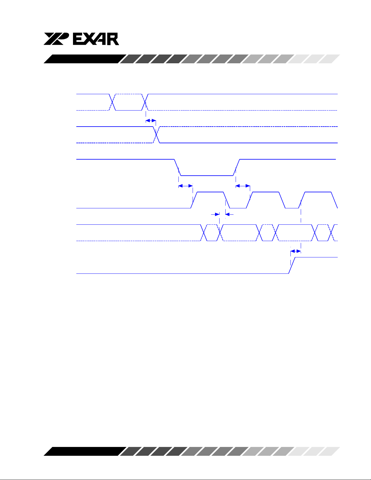
ST16C450
-IOW
IOW
-RTS
-DTR
-CD
-CTS
-DSR
INT
-IOR
IOR
-RI
Active
Change of state
T17d
Change of state
Change of state
T18d T18d
Active Active
T19d
Active
Change of state
Active
Active Active
T18d
Change of state
Rev. 4.20
X450-MD-1
Modem input/output timing
23
Page 24
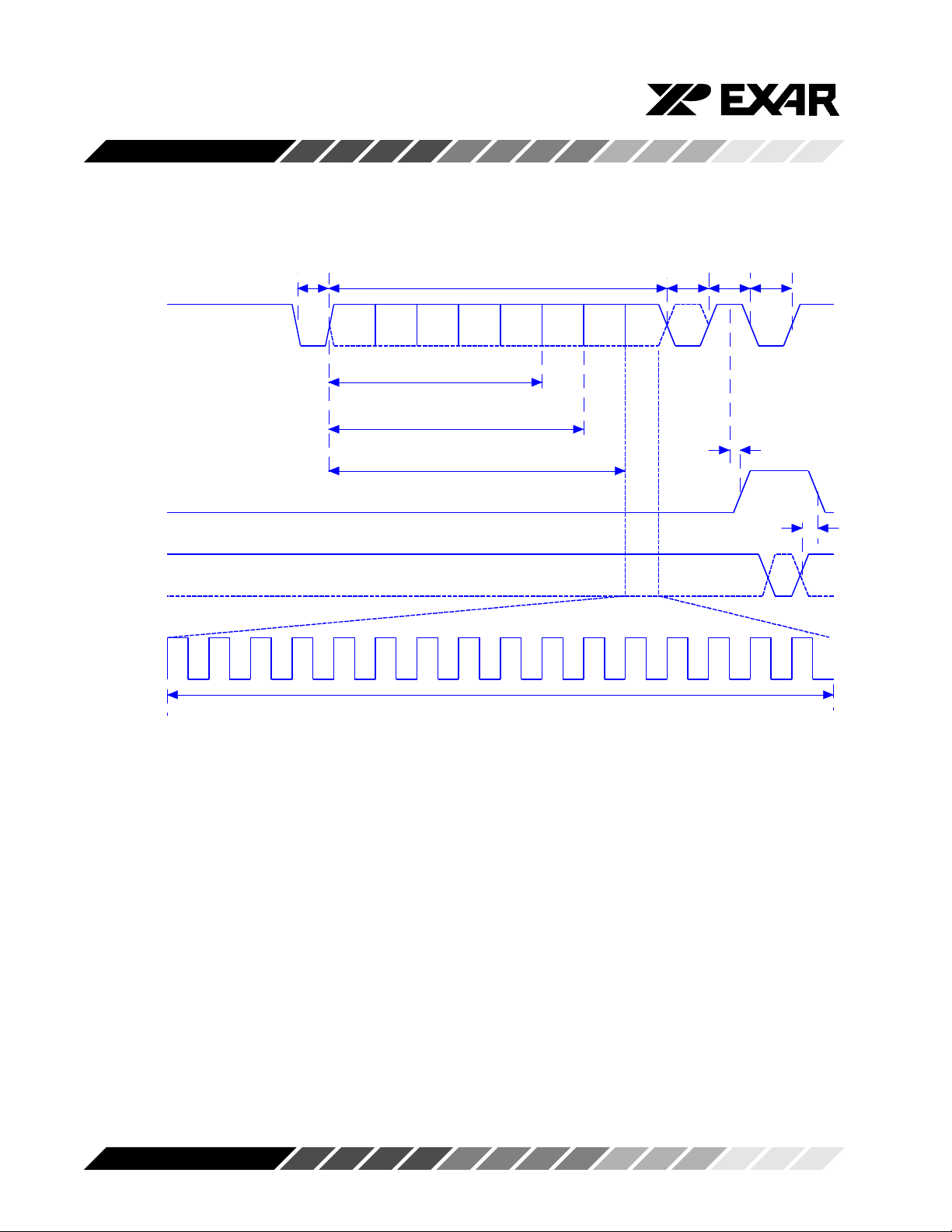
ST16C450
RX
INT
-IOR
IOR
START
BIT
DATA BITS (5-8)
D0 D1 D2 D3 D4 D5 D6 D7
5 DATA BITS
6 DATA BITS
7 DATA BITS
PARITY
BIT
STOP
BIT
NEXT
DATA
START
BIT
T20d
Active
T21d
Rev. 4.20
16 BAUD RATE CLOCK
Receive timing
X450-RX-1
24
Page 25
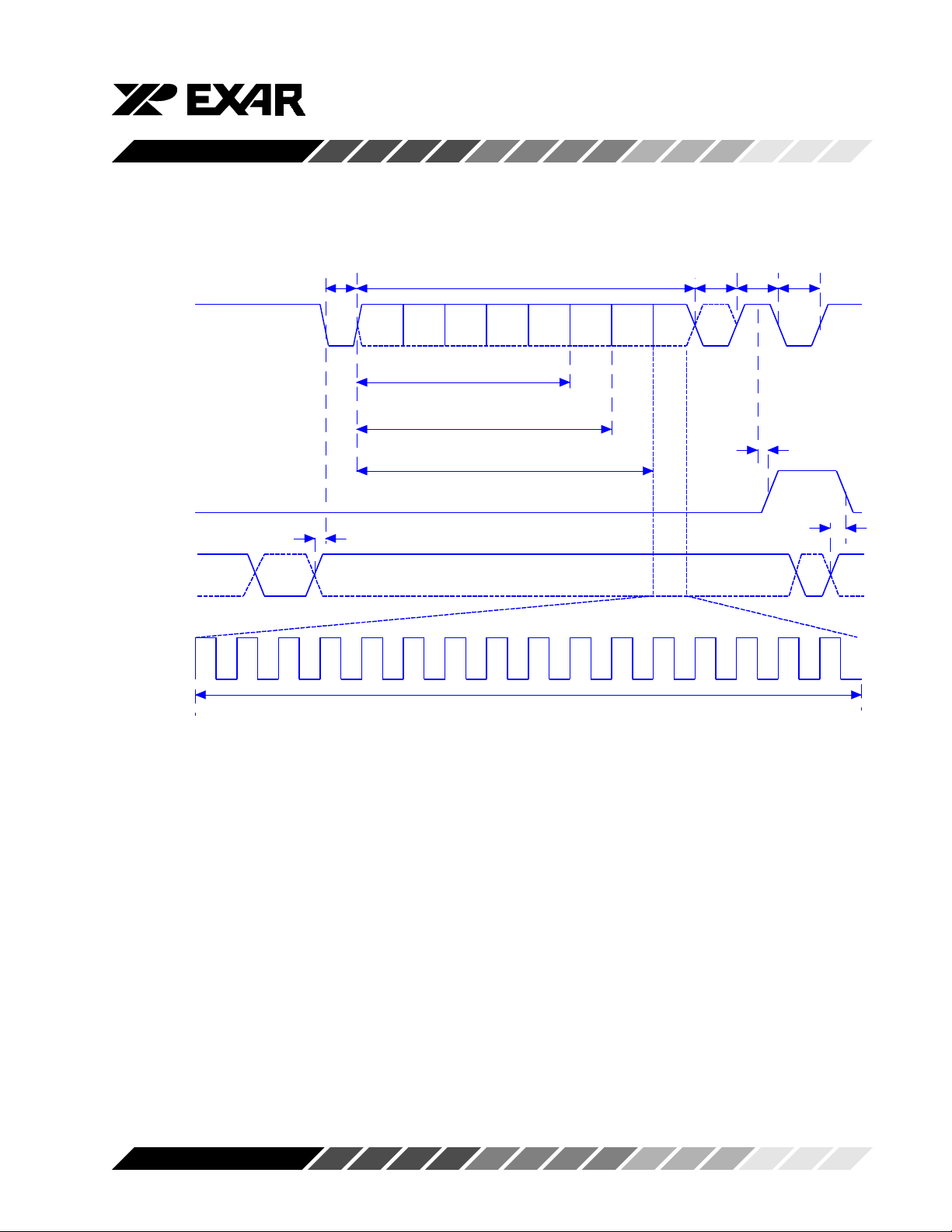
ST16C450
TX
INT
-IOW
IOW
Active
START
BIT
DATA BITS (5-8)
D0 D1 D2 D3 D4 D5 D6 D7
5 DATA BITS
6 DATA BITS
7 DATA BITS
T23d
PARITY
BIT
STOP
BIT
NEXT
DATA
START
BIT
T22d
Active
Tx Ready
T24d
Active
Rev. 4.20
16 BAUD RATE CLOCK
Transmit timing
X450-TX-1
25
Page 26
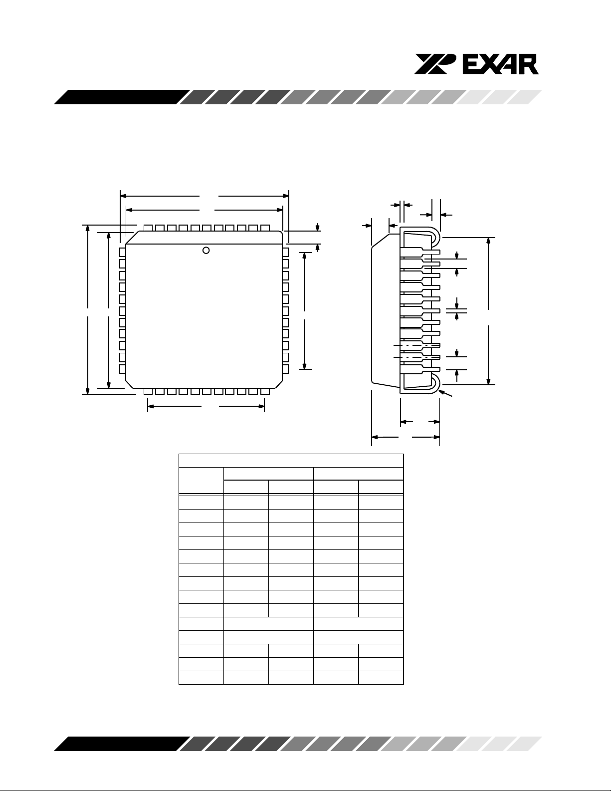
ST16C450
PACKAGE OUTLINE DRAWING
D D
44LEAD PLASTIC LEADED CHIP CARRIER
(PLCC)
D
D
1
1
244
1
D
3
D
3
45° x H
45° x H
2
C
1
A
A
1
Seating Plane
A
2
B
1
B
e
R
D
2
Note: The control dimension is the inch column
SYMBOL
A
A
1
A
2
B
B
1
C
D
D
1
D
2
D
3
e
H
1
H
2
R
INCHES MILLIMETERS
MIN MAX MIN MAX
0.165
0.090
0.020
0.013
0.026
0.008
0.685
0.650
0.590
0.042
0.042
0.025
0.500 typ
0.50 BSC
0.180
0.120
-----
0.021
0.032
0.013
0.695
0.656
0.630
0.056
0.048
0.045
4.19
2.29
0.51
0.33
0.66
0.19
17.40
16.51
14.99
12.70 typ
1.27BSC
1.07
1.07
0.64
4.57
3.05
------
0.53
0.81
0.32
17.65
16.66
16.00
1.42
1.22
1.14
Rev. 4.20
26
Page 27
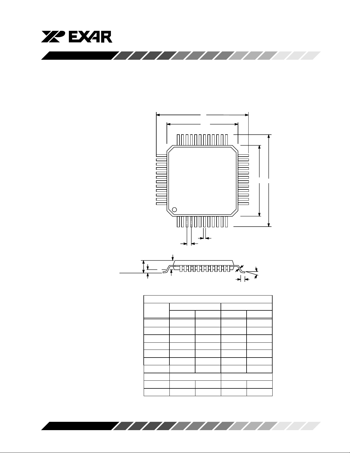
PACKAGE OUTLINE DRAWING
48 LEAD THIN QUAD FLAT PACK
(TQFP)
D
D
36 25
1
ST16C450
Seating
Plane
37
48
1
B
e
A
2
A
A
1
1
2
Note: The control dimension is the millimeter column
SYMBOL
A
A
1
A
2
B
C
D
D
1
e
L
α
INCHES MILLIMETERS
MIN MAX MIN MAX
0.039
0.002
0.037
0.007
0.004
0.346
0.272
0.047
0.006
0.041
0.011
0.008
0.362
0.280
1.00
0.05
0.95
0.17
0.09
8.80
6.90
0.20 BSC
0.018
0°
0.030
7°
0.45
0°
C
L
0.50BSC
24
13
D
1.20
0.15
1.05
0.27
0.20
9.20
7.10
0.75
7°
D
1
α
Rev. 4.20
27
Page 28
ST16C450
EXPLANATION OF DATA SHEET REVISIONS:
FROM TO CHANGES DATE
4.10 4.20 Added revision history. Added Device Status to front page. Sept 2003
NOTICE
EXAR Corporation reserves the right to make changes to the products contained in this publication in order to
improve design, performance or reliability. EXAR Corporation assumes no responsibility for the use of any circuits
described herein, conveys no license under any patent or other right, and makes no representation that the circuits
are free of patent infringement. Charts and schedules contained here in are only for illustration purposes and may
vary depending upon a user's specific application. While the information in this publication has been carefully
checked; no responsibility, however, is assumed for inaccuracies.
EXAR Corporation does not recommend the use of any of its products in life support applications where the failure
of the product can reasonably be expected to cause failure of the life support system or to significantly affect its
safety or effectiveness. Products are not authorized for use in such applications unless EXAR Corporation receives,
in writing, assurances to its satisfaction that: (a) the risk of injury or damage has been minimized; (b) the user
assumes all such risks; (c) potential liability of EXAR Corporation is adequately protected under the circumstances.
Copyright 2003 EXAR Corporation
Datasheet September 2003
Send your UART technical inquiry with technical details to hotline:
Reproduction, in part or whole, without prior written consent of EXAR Corporation is prohibited.
Rev. 4.20
28
 Loading...