

SA12B5
Application SpecificDiscretes
A.S.D.
MAINAPPLICATIONS
Any electronic equipment where suitable bus
termination is required to avoid signal reflections
anddistortions:
PCs
Workstations
High frequencyprocessorboards
Dataline interface
DESCRIPTION
Dedicatedto bus termination,the Schottkyarrays
SA12B5, SA16B3 and SA16B6 minimise stray
emissions from PCB tracks. Theyprovide suitable
termination by avoiding signal reflexions and
distortions.
FEATURES
12-BIT (SA12) OR 16-BIT (SA16) DUAL
SCHOTTKYDIODE ARRAYS
REVERSEVOLTAGE: V
FORWARDVOLTAGEV
TM
RRM
< 1.3V
F
=7.5 V
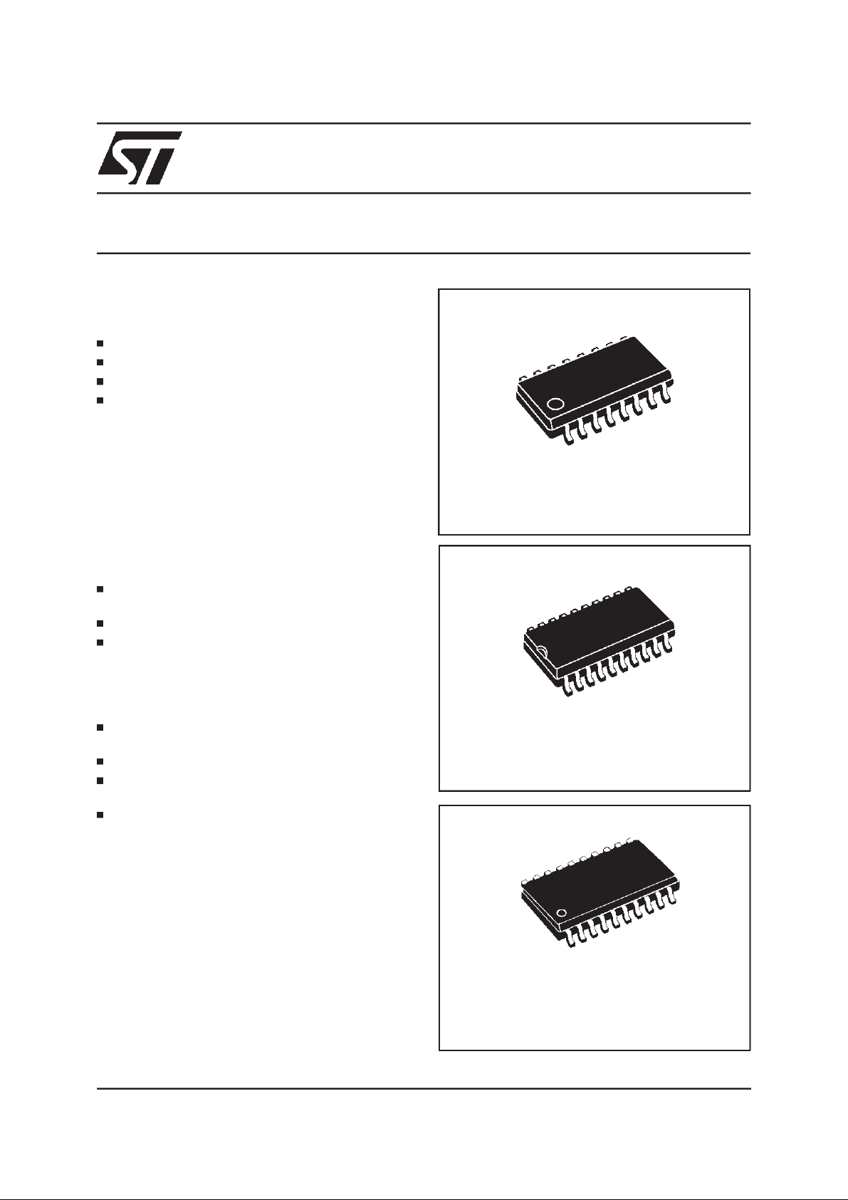
SA16B3 / SA16B6
SCHOTTKYARRAYS
SO-16
BENEFITS
Provides impedance matching, and minimizes
distortion.
LowersEMI /RFI radiation.
Eliminates negative voltage : minimizes risk of
latch-upfor sensitiveICs.
Savesvaluable spaceon board.
COMPLIESWITH FOLLOWINGSTANDARD:
-MIL STD 883C - Method3015-6 - class3
-IEC1000-4-2 level 4
April 1999 - Ed:1
SO-20
SSOP20
1/5
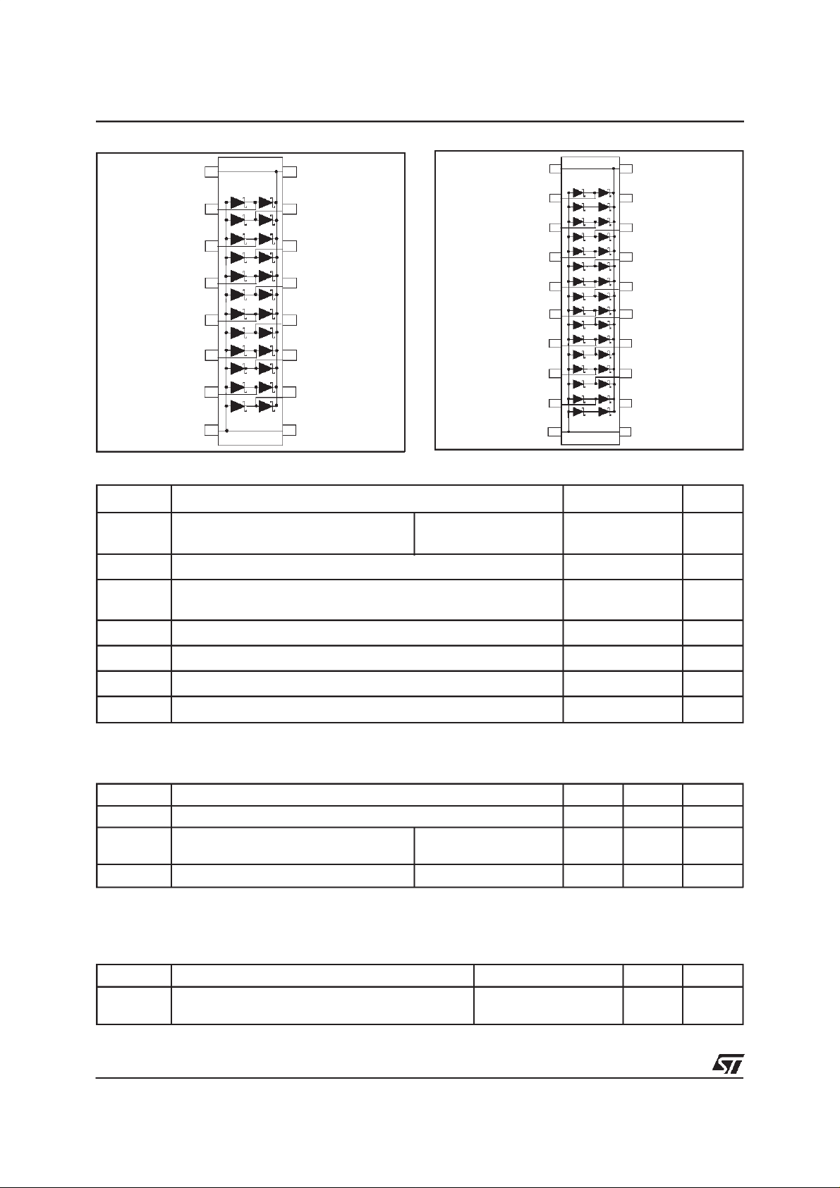
SA12B5 / SA16B3 / SA16B6
FUNCTIONAL DIAGRAM
(SO-16)
FUNCTIONALDIAGRAM
(SO-20and SSOP20)
1
V
CC
2
3
4
5
6
7
8
V
SS
V
16
CC
15
14
13
12
11
10
V
9
SS
ABSOLUTE MAXIMUMRATINGS(T
amb
=25°C)
V
CC
120
2
3
4
5
615
7
8
912
V
SS
10
V
CC
19
18
17
16
14
13
V
11
SS
Symbol Parameterand test conditions Value Unit
P Powerdissipation SO-20
SO-16and SSOP20
V
OP
V
PP
Maximumoperatingvoltage(VCC-VSS)
Maximumelectrostatic discharge
1250
mW
850
7.5 V
8kV
MILSTD 883C- Method3015-6/ IEC1000-4-2contact
T
op
T
stg
T
L
T
Note1: withintheToprange,the SAxxkeepon operating.Theimpactsoftheambienttemperaturearegivenbyderatingcurveson thefollowingpage.
Operatingtemperaturerange (seenote 1)
Storagetemperaturerange
Maximumlead temperaturefor solderingduring 10s
j
Maximumjunction temperature
-40to +85 °C
-55 to+150 °C
260 °C
150 °C
ELECTRICALCHARACTERISTICS (T
amb
=25°C)
Symbol Parameterand test conditions Typ. Max. Unit
I
R
V
F
Leakagecurrent@ V
Forwardvoltage
(seenote 2)
C
d
Note 2: for both pull-up and pull-down schottydiodes.
Capacitance V
RRM
= 7.5V
5
IPP= 18 mA
I
=50mA
PP
=0V, F =1MHz 16 pF
bias
1.05
1.3
THERMAL RESISTANCE
Symbol Parameter Packages Value Unit
2/5
R
th(j-a)
Junctionto ambient SO-16and SSOP20
SO-20
140
100
µ
A
V
°C/W

Fig1-1:
Clamping forward voltage versus peak
pulse current(typical values,lowlevel).
SA12B5 / SA16B3 / SA16B6
Fig1-2:
pulsecurrent (typical values,highlevel).
Clamping forward voltage versus peak
Ipp(A)
1E+0
tp=2.5µs
Tj=25°C
1E-1
1E-2
Tj=85°C
1E-3
Tj=-40°C
Vcl(V)
1E-4
0.0 0.2 0.4 0.6 0.8 1.0 1.2 1.4 1.6 1.8 2.0
Fig 2: Leakage current versus junction temperature(typicalvalues).
IR(µA)
1E+2
VR=7.5V
1E+1
1E+0
Ipp(A)
5.0
Tj=25°C
tp=2.5µs
1.0
Vcl(V)
0.1
01234567
Fig 3: Non repetitive surge peak forward current
versuspulseduration (rectangularwaveform).
IFSM(A)
10
5
Tj initial =25°C
1E-1
1E-2
0 25 50 75 100 125
Fig 4:
Non repetitive surge peak forward current
Tj(°C)
versusinitialjunctiontemperature.
IFSM[Tj] / IFSM[Tj=25°C]
1.2
1.0
0.8
0.6
0.4
0.2
0.0
0 25 50 75 100 125
Tj(°C)
2
tp(µs)
1
1 10 100 1000
Fig 5:
Capacitance between input or output and
groundversusapplied voltage (typical values).
Ci/o(pF)
30
Vcc=5V
F=1MHz
28
Vosc=30mV
26
24
22
20
18
16
0.0 0.5 1.0 1.5 2.0 2.5 3.0 3.5 4.0 4.5 5.0 5.5 6.0
Vi/o-gnd(V)
3/5

SA12B5 / SA16B3 / SA16B6
TYPICALAPPLICATION
VCC
SAxxBx
µP
Bus
MARKING
Type Package Marking
SA12B5 SO16 SA12B5
SA16B3 SO20 SA16B3
SA16B6 SSOP20 SA16B6
PACKAGE MECHANICALDATA
SO-16
L
Aa2
b
e3
D (1)
16
e
9
81
S
M
F (1)
Weight: 0.160g
G
c1
C
a1
E
(1) Do not include mold
flash or protrusions. Mold
flash or protrusions shall
not exceed0.15mm
(0.006inches)
High speed
memory
DIMENSIONS
REF.
Millimeters Inches
Min. Typ. Max. Min. Typ. Max.
A 1.75 0.069
b1
a1 0.1 0.20 0.004 0.008
a2 1.6 0.063
b 0.35 0.46 0.014 0.018
b1 0.19 0.25 0.007 0.010
C 0.5 0.020
c1 45°(typ.)
D 9.8 10 0.386 0.394
E 5.8 6.2 0.228 0.244
e 1.27 0.050
e3 8.89 0.350
F 3.8 4.0 0.150 0.158
G 4.6 5.3 0.181 0.209
L 0.5 1.27 0.020 0.050
M 0.75 0.030
S8°(typ.)
4/5

PACKAGEMECHANICAL DATA
SO-20
Weight: 0.520g
SSOP20
SA12B5 / SA16B3 / SA16B6
DIMENSIONS
REF.
A 2.35 2.65 0.092 0.104
A1 0.10 0.20 0.004 0.008
B 0.33 0.51 0.013 0.020
C 0.23 0.32 0.009 0.013
D 12.6 13.0 0.484 0.512
E 7.40 7.60 0.291 0.299
e 1.27 0.050
H 10.0 10.65 0.394 0.419
h 0.25 0.75 0.010 0.029
L 0.50 1.27 0.020 0.050
K8°(max)
Millimeters Inches
Min. Typ. Max. Min. Typ. Max.
DIMENSIONS
L
REF.
Millimeters Inches
Min. Typ. Max. Min. Typ. Max.
Aa2
b
D
e
S
a1
E
b1
A 2.00 0.079
A1 0.25 0.010
A2 1.51 2.00 0.059 0.079
b 0.25 0.30 0.35 0.010 0.012 0.014
c 0.10 0.35 0.004 0.014
20
11
F
101
D 7.05 8.05 0.278 0.317
E 7.60 8.70 0.299 0.343
E1 5.02 6.10 6.22 0.198 0.240 0.245
e 0.65 0.026
k0° 10° 0° 10°
L 0.25 0.50 0.80 0.010 0.020 0.031
Weight: 0.180g
Informationfurnishedis believedto be accurate and reliable. However, STMicroelectronics assumes no responsibilityfor the consequences of
use of suchinformation norforany infringementof patents or otherrights of thirdparties which may resultfromits use. No license isgranted by
implication or otherwise under any patent or patent rights of STMicroelectronics. Specifications mentioned in thispublication are subject to
change without notice. This publication supersedes andreplaces allinformationpreviouslysupplied.
STMicroelectronics products are not authorized for use as criticalcomponents in life support devices orsystems withoutexpress written approval of STMicroelectronics.
The ST logo isa registered trademark of STMicroelectronics
1999 STMicroelectronics- Printedin Italy- All rights reserved.
STMicroelectronics GROUP OF COMPANIES
Australia - Brazil - Canada - China -France - Germany - Italy -Japan - Korea - Malaysia - Malta - Mexico -Morocco -
The Netherlands - Singapore - Spain - Sweden - Switzerland - Taiwan - Thailand - United Kingdom -U.S.A.
http://www.st.com
5/5
 Loading...