

SGS Thomson Microelectronics PSD935G2, PSD935G2V Datasheet
1/3
PRELIMINARY DATA
January 2002
This is preliminary information on a new product now in development or undergoing evaluation. Details are subject to change without notice.
PSD935G2
Confi gurabl e Memory Syst em on a C hi p
for 8-Bit Microcontrollers
FEATURES SUMMARY
■ 5 V±10% Single Supply Voltage:
■ Up to 4 Mbit of Primary Flash Memory (8
uniform sectors)
■ 256Kbit Secondary Flash Memory (4 uniform
sectors)
■ Up to 64 Kbit SRAM
■ Over 3,000 Gates of PLD: DPLD
■ 52 Reconfigurable I/O ports
■ Enhanced JTAG Serial Port
■ Programmable power management
■ High Endurance:
– 100,000 Erase/Write Cycles of Flash Memory
– 1,000 Erase/Write Cycles of PLD
Figure 1. Packages
TQFP80 (U)
1
1.0
Introduction
PSD9XX Family
PSD935G2
Configurable Memory System on a Chip
for 8-Bit Microcontrollers
The PSD9XX series of Programmable Microcontroller (MCU) Peripherals brings
In-System-Programmability (ISP) to Flash memory and programmable logic. The result is a
simple and flexible solution for embedded designs. PSD9XX devices combine many of the
peripheral functions found in MCU based applications:
• 4 Mbit of Flash memory
• A secondary Flash memory for boot or data
• Over 3,000 gates of Flash programmable logic
• 64 Kbit SRAM
• Reconfigurable I/O ports
• Programmable power management.

PSD9XX Family PSD935G2
2
1.0
Introduction
(Cont.)
Please refer to the revision block at the end of this
document for updated information.
The PSD935G2 device offers two methods to program PSD Flash memory while the PSD
is soldered to a circuit board.
❏ In-System Programming (ISP) via JTAG
An IEEE 1149.1 compliant JTAG-ISP interface is included on the PSD enabling the
entire device (both flash memories, the PLD, and all configuration) to be rapidly
programmed while soldered to the circuit board. This requires no MCU participation,
which means the PSD can be programmed anytime, even while completely blank.
The innovative JTAG interface to flash memories is an industry first, solving key
problems faced by designers and manufacturing houses, such as:
• First time programming – How do I get firmware into the flash the very first time?
JTAG is the answer, program the PSD while blank with no MCU involvement.
• Inventory build-up of pre-programmed devices – How do I maintain an accurate
count of pre-programmed flash memory and PLD devices based on customer
demand? How many and what version? JTAG is the answer, build your hardware
with blank PSDs soldered directly to the board and then custom program just before
they are shipped to customer. No more labels on chips and no more wasted
inventory.
• Expensive sockets – How do I eliminate the need for expensive and unreliable
sockets? JTAG is the answer. Solder the PSD directly to the circuit board. Program
first time and subsequent times with JTAG. No need to handle devices and bend the
fragile leads.
❏ In-Application re-Programming (IAP)
Two independent flash memory arrays are included so the MCU can execute code
from one memory while erasing and programming the other. Robust product firmware
updates in the field are possible over any communication channel (CAN, Ethernet,
UART, J1850, etc) using this unique architecture. Designers are relieved of these
problems:
• Simultaneous read and write to flash memory – How can the MCU program the
same memory from which it is executing code? It cannot. The PSD allows the MCU
to operate the two flash memories concurrently, reading code from one while erasing
and programming the other during IAP.
• Complex memory mapping – How can I map these two memories efficiently?
A Programmable Decode PLD is embedded in the PSD. The concurrent PSD
memories can be mapped anywhere in MCU address space, segment by segment
with extremely high address resolution. As an option, the secondary flash memory
can be swapped out of the system memory map when IAP is complete. A built-in
page register breaks the MCU address limit.
• Separate program and data space – How can I write to flash memory while it
resides in “program” space during field firmware updates, my 80C51 won’t allow it
The flash PSD provides means to “reclassify” flash memory as “data” space during
IAP, then back to “program” space when complete.
PSDsoft – ST’s software development tool – guides you through the design
process step-by-step making it possible to complete an embedded MCU design
capable of ISP/IAP in just hours. Select your MCU and PSDsoft will take you through
the remainder of the design with point and click entry, covering...PSD selection, pin
definitions, programmable logic inputs and outputs, MCU memory map definition, ANSI C
code generation for your MCU, and merging your MCU firmware with the PSD design.
When complete, two different device programmers are supported directly from PSDsoft –
FlashLINK (JTAG) and PSDpro.
The PSD935G2 is available in an 80-pin TQFP package.

PSD935G2 PSD9XX Family
❏ A simple interface to 8-bit microcontrollers that use either multiplexed or
non-multiplexed busses. The bus interface logic uses the control signals generated by
the microcontroller automatically when the address is decoded and a read or write is
performed. A partial list of the MCU families supported include:
• Intel 8031, 80196, 80188, 80C251
• Motorola 68HC11 and 68HC16
• Philips 8031 and 80C51XA
• Zilog Z80, Z8 and Z180
• Infineon C500 family
❏ 4 Mbit Flash memory. This is the main Flash memory. It is divided into eight
equal-sized blocks that can be accessed with user-specified addresses.
❏ Internal secondary 256 Kbit Flash boot memory. It is divided into four equal-sized
blocks that can be accessed with user-specified addresses. This secondary memory
brings the ability to execute code and update the main Flash concurrently.
❏ 64 Kbit SRAM. The SRAM’s contents can be protected from a power failure by
connecting an external battery.
❏ General Purpose PLD (GPLD) with 24 outputs. The GPLD may be used to implement
external chip selects or combinatorial logic function.
❏ Decode PLD (DPLD) that decodes address for selection of internal memory blocks.
❏ 52 individually configurable I/O port pins that can be used for the following functions:
• MCU I/Os
• PLD I/Os
• Latched MCU address output
• Special function I/Os.
• I/O ports may be configured as open-drain outputs.
❏ Standby current as low as 50 µA for 5 V devices.
❏ Built-in JTAG compliant serial port allows full-chip In-System Programmability (ISP).
With it, you can program a blank device or reprogram a device in the factory or the field.
❏ Internal page register that can be used to expand the microcontroller address space
by a factor of 256.
❏ Internal programmable Power Management Unit (PMU) that supports a low power
mode called Power Down Mode. The PMU can automatically detect a lack of
microcontroller activity and put the PSD9XX into Power Down Mode.
❏ Erase/Write cycles:
• Flash memory – 100,000 minimum
• PLD – 1,000 minimum
2.0
Key Features
3
3.0 PSD9XX
Series
Part # Flash
Flash Main Boot
Serial ISP Memory Memory
PSD9XX I/O PLD Input Output PLD JTAG/ISP Kbit Kbit SRAM Supply
Series Device Pins Inputs Macrocells Macrocells Outputs Port 8 Sectors (4 Sectors) Kbit Voltage
PSD935G2 52 66 24 Yes 4096 256 64 5V
PSD9XX PSD913G2 27 57 19 Yes 1024 256 16 5V
PSD934F2 27 57 19 Yes 2048 256 64 5V
Table 1. PSD9XX Product Matrix
PSD9XX Family PSD935G2
4
PROG.
MCU BUS
INTRF.
ADIO
PORT
CNTL0,
CNTL1,
CNTL2
AD0 – AD15
*
PLD
INPUT
BUS
PROG.
PORT
PORT
A
PROG.
PORT
PORT
B
POWER
MANGMT
UNIT
4 MBIT MAIN FLASH
MEMORY
8 SECTORS
VSTDBY
PA0 – PA7
PROG.
PORT
PORT
F
PROG.
PORT
PORT
G
PROG.
PORT
PORT
E
PB0 – PB7
PROG.
PORT
PORT
C
PROG.
PORT
PORT
D
PF0 – PF7
PG0 – PG7
PE0 – PE7
PC0 – PC7
PD0 – PD3
ADDRESS/DATA/CONTROL BUS
66
66
256 KBIT SECONDARY
FLASH MEMORY
(BOOT OR DATA)
4 SECTORS
64 KBIT BATTERY
BACKUP SRAM
RUNTIME CONTROL
AND I/O REGISTERS
SRAM SELECT
GPLD OUTPUT
GPLD OUTPUT
GPLD OUTPUT
I/O PORT PLD INPUT
CSIOP
FLASH ISP PLD
(GPLD)
FLASH DECODE
PLD (DPLD
)
PLD, CONFIGURATION
& FLASH MEMORY
LOADER
JTAG
SERIAL
CHANNEL
(
PE6
)
PAGE
REGISTER
EMBEDDED
ALGORITHM
SECTOR
SELECTS
SECTOR
SELECTS
GLOBAL
CONFIG. &
SECURITY
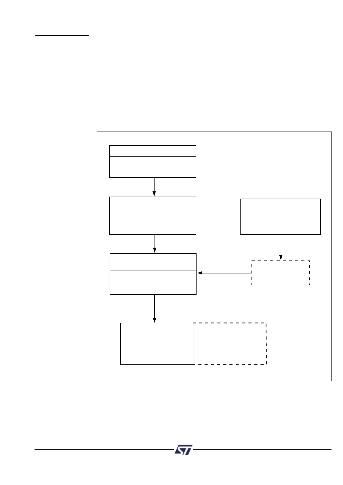
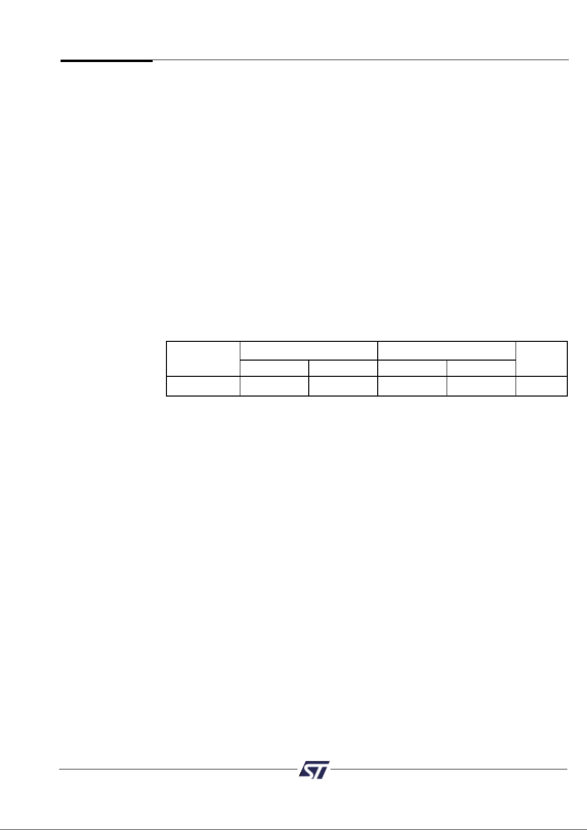
Figure 1. PSD935G2 Block Diagram
*Additional address lines can be brought into PSD via Port A, B, C, D, or F.

PSD935G2 PSD9XX Family
5
PSD9XX devices contain several major functional blocks. Figure 1 on page 3 shows the
architecture of the PSD9XX device family. The functions of each block are described
briefly in the following sections. Many of the blocks perform multiple functions and are user
configurable.
4.1 Memory
The PSD935G2 contains the following memories:
• 4 Mbit Flash
• A secondary 256 Kbit Flash memory for boot or data
• 64 Kbit SRAM.
Each of the memories is briefly discussed in the following paragraphs. A more detailed
discussion can be found in section 9.
The 4 Mbit Flash is the main memory of the PSD935G2. It is divided into eight
equally-sized sectors that are individually selectable.
The 256 Kbit secondary Flash memory is divided into four equally-sized sectors. Each
sector is individually selectable.
The 64 Kbit SRAM is intended for use as a scratchpad memory or as an extension to the
microcontroller SRAM. If an external battery is connected to the PSD9XX’s Vstby pin, data
will be retained in the event of a power failure.
Each block of memory can be located in a different address space as defined by the user.
The access times for all memory types includes the address latching and DPLD decoding
time.
4.2 PLDs
The device contains two PLD blocks, each optimized for a different function, as shown in
Table 2. The functional partitioning of the PLDs reduces power consumption, optimizes
cost/performance, and eases design entry.
The Decode PLD (DPLD) is used to decode addresses and generate chip selects for
the PSD935G2 internal memory and registers. The General Purpose PLD (GPLD) can
implement user-defined external chip selects and logic functions. The PLDs receive their
inputs from the PLD Input Bus and are differentiated by their output destinations, number
of Product Terms.
The PLDs consume minimal power by using Zero-Power design techniques. The speed
and power consumption of the PLD is controlled by the Turbo Bit in the PMMR0 register
and other bits in the PMMR2 registers. These registers are set by the microcontroller at
runtime. There is a slight penalty to PLD propagation time when invoking the non-Turbo
bit.
4.3 I/O Ports
The PSD935G2 has 52 I/O pins divided among seven ports (Port A, B, C, D, E, F and G).
Each I/O pin can be individually configured for different functions. Ports can be configured
as standard MCU I/O ports, PLD I/O, or latched address outputs for microcontrollers using
multiplexed address/data busses.
The JTAG pins can be enabled on Port E for In-System Programming (ISP). Ports F and
G can also be configured as a data port for a non-multiplexed bus.
4.4 Microcontroller Bus Interface
The PSD935G2 easily interfaces with most 8-bit microcontrollers that have either
multiplexed or non-multiplexed address/data busses. The device is configured to respond
to the microcontroller’s control signals, which are also used as inputs to the PLDs. Section
9.3.5 contains microcontroller interface examples.
4.0
PSD9XX
Architectural
Overview
Name Abbreviation Inputs Outputs Product Terms
Decode PLD DPLD 66 15 40
General PLD GPLD 66 24 136
Table 2. PLD I/O Table
PSD9XX
Architectural
Overview
(cont.)
4.5 ISP via JTAG Port
In-System Programming can be performed through the JTAG pins on Port E. This serial
interface allows complete programming of the entire PSD935G2 device. A blank device
can be completely programmed. The JTAG signals (TMS, TCK, TSTAT, TERR, TDI, TDO)
can be multiplexed with other functions on Port E. Table 3 indicates the JTAG signals pin
assignments.
4.6 In-System Programming (ISP)
Using the JTAG signals on Port E, the entire PSD935G2 (memory, logic, configuration)
device can be programmed or erased without the use of the microcontroller.
Port E Pins JTAG Signal
PE0 TMS
PE1 TCK
PE2 TDI
PE3 TDO
PE4 TSTAT
PE5 TERR
Table 3. JTAG Signals on Port E
PSD9XX Family PSD935G2
6
4.7 In-Application re-Programming (IAP)
The main Flash memory can also be programmed in-system by the microcontroller
executing the programming algorithms out of the secondary Flash memory, or SRAM.
Since this is a sizable separate block, the application can also continue to operate. The
secondary Flash boot memory can be programmed the same way by executing out of the
main Flash memory. Table 4 indicates which programming methods can program different
functional blocks of the PSD9XX.
Device
Functional Block JTAG-ISP Programmer IAP
Main Flash memory Yes Yes Yes
Flash Boot memory Yes Yes Yes
PLD Array (DPLD and GPLD) Yes Yes No
PSD Configuration Yes Yes No
Table 4. Methods of Programming Different Functional Blocks of the PSD935G2
4.8 Page Register
The eight-bit Page Register expands the address range of the microcontroller by up to
256 times.The paged address can be used as part of the address space to access
external memory and peripherals or internal memory and I/O. The Page Register can also
be used to change the address mapping of blocks of Flash memory into different memory
spaces for IAP.
4.9 Power Management Unit
The Power Management Unit (PMU) in the PSD935G2 gives the user control of the
power consumption on selected functional blocks based on system requirements. The
PMU includes an Automatic Power Down unit (APD) that will turn off device functions due
to microcontroller inactivity. The APD unit has a Power Down Mode that helps reduce
power consumption.
The PSD935G2 also has some bits that are configured at run-time by the MCU to reduce
power consumption of the GPLD. The turbo bit in the PMMR0 register can be turned off
and the GPLD will latch its outputs and go to standby until the next transition on its inputs.
Additionally, bits in the PMMR2 register can be set by the MCU to block signals from
entering the GPLD to reduce power consumption. See section 9.5.
PSD935G2 PSD9XX Family
7
Merge MCU Firmware
with PSD Configuration
ST
PSD Programmer
*.OBJ FILE
Define PSD Pin and
Node functions
Point and click definition of
PSD pin functions, internal nodes,
and MCU system memory map.
Choose MCU and PSD
Automatically Configures MCU
bus interface and other PSD
attributes.
PSDPro or
FlashLink (JTAG)
A composite object file is created
containing MCU firmware and
PSD configuration.
C Code Generation
Generate C Code
Specific to PSD
Functions
User's choice of
Microcontroller
Compiler/Linker
*.OBJ file
available
for 3rd party
programmers
(Conventional or JTAG-ISP)
MCU Firmware
Hex or S-Record
format
Figure 2. PSDsoft Development Tool
5.0
Development
System
The PSD9XX series is supported by PSDsoft a Windows-based (95, 98, NT) software
development tool. A PSD design is quickly and easily produced in a point and click
environment. The designer does not need to enter Hardware Definition Language (HDL)
equations (unless desired) to define PSD pin functions and memory map information. The
general design flow is shown in Figure 2 below. PSDsoft is available from our web site
(www.st.com/psm) or other distribution channels.
PSDsoft directly supports two low cost device programmers from ST. PSDpro
and FlashLINK (JTAG). Both of these programmers may be purchased through your local
rep/distributor, or directly from our web site using a credit card. The PSD9XX is also
supported by third party device programmers, see web site for current list.
PSD9XX Family PSD935G2
8
The following table describes the pin names and pin functions of the PSD935G2. Pins that
have multiple names and/or functions are defined using PSD Configuration.
6.0
Table 5.
PSD935G2
Pin
Descriptions
Pin*
(TQFP
Pin Name Pkg.) Type Description
ADIO0-7 3-7 I/O This is the lower Address/Data port. Connect your MCU
10-12 address or address/data bus according to the following rules:
1. If your MCU has a multiplexed address/data bus where the
data is multiplexed with the lower address bits, connect
AD[0:7] to this port.
2. If your MCU does not have a multiplexed address/data bus,
connect A[0:7] to this port.
3. If you are using an 80C51XA in burst mode, connect
A4/D0 through A11/D7 to this port.
ALE or AS latches the address. The PSD drives data out only
if the read signal is active and one of the PSD functional blocks
was selected. The addresses on this port are passed to the
PLDs.
ADIO8-15 13-20 I/O This is the upper Address/Data port. Connect your MCU
address or address/data bus according to the following rules:
1. If your MCU has a multiplexed address/data bus where the
data is multiplexed with the lower address bits, connect
A[8:15 ] to this port.
2. If your MCU does not have a multiplexed address/data bus,
connect A[8:15 ] to this port.
3. If you are using an 80C251 in page mode, connect AD[8:15]
to this port
4. If you are using an 80C51XA in burst mode, connect
A[12:19] to this port.
ALE or AS latches the address. The PSD drives data out only
if the read signal is active and one of the PSD functional
blocks was selected. The addresses on this port are passed
to the PLDs.
CNTL0 59 I The following control signals can be connected to this port,
based on your MCU:
1. WR — active-low write input.
2. R_W — active-high read/active low write input.
This pin is connected to the PLDs. Therefore, these signals can
be used in decode and other logic equations.
CNTL1 60 I The following control signals can be connected to this port,
based on your MCU:
1. RD — active-low read input.
2. E — E clock input.
3. DS — active-low data strobe input.
4. PSEN — connect PSEN to this port when it is being used as
an active-low read signal. For example, when the 80C251
outputs more than 16 address bits, PSEN is actually the read
signal.
This pin is connected to the PLDs. Therefore, these signals can
be used in decode and other logic equations.
CNTL2 40 I This pin can be used to input the PSEN (Program Select
Enable) signal from any MCU that uses this signal for code
exclusively. If your MCU does not output a Program Select
Enable signal, this port can be used as a generic input. This
port is connected to the PLD as input.
Reset 39 I Active low input. Resets I/O Ports, PLD Micro
⇔Cells, some of
the configuration registers and JTAG registers. Must be active
at power up. Reset also aborts the Flash programming/erase
cycle that is in progress.
PSD935G2 PSD9XX Family
Pin*
(TQFP
Pin Name Pkg.) Type Description
PA0-PA7 51-58 I/O Port A, PA0-7. This port is pin configurable and has multiple
CMOS functions:
or Open 1. MCU I/O — standard output or input port
Drain 2. GPLD output.
3. Input to the PLD.
PB0-PB7 61-68 I/O Port B, PB0-7. This port is pin configurable and has multiple
CMOS functions:
or Open 1. MCU I/O — standard output or input port.
Drain 2. GPLD output.
3. Input to the PLD.
PC0-PC7 41-48 I/O Port C, PC0-7. This port is pin configurable and has multiple
CMOS functions:
or Slew 1. MCU I/O — standard output or input port.
Rate 2. External chip select (ECS0-7) output.
3. Input to the PLD.
PD0 79 I/O Port D pin PD0 can be configured as:
CMOS 1. ALE or AS input — latches addresses on ADIO0-15 pins
or Open 2. AS input — latches addresses on ADIO0-15 pins on the
Drain rising edge.
3. Input to the PLD.
4. Transparent PLD input.
PD1 80 I/O Port D pin PD1 can be configured as:
CMOS 1. MCU I/O
or Open 2. Input to the PLD.
Drain 3. CLKIN clock input — clock input to the GPLD
Micro⇔Cells, the APD power down counter and GPLD
AND Array.
PD2 1 I/O Port D pin PD2 can be configured as:
CMOS 1. MCU I/O
or Open 2. Input to the PLD.
Drain 3. CSI input — chip select input. When low, the CSI enables
the internal PSD memories and I/O. When high, the
internal memories are disabled to conserve power. CSI
trailing edge can get the part out of power-down mode.
PD3 2 I/O
Port D pin PD3 can be configured as:
CMOS
1. MCU I/O
or Open
2. Input to the PLD.
Drain
PE0 71 I/O Port E, PE0. This port is pin configurable and has multiple
CMOS functions:
or Open 1. MCU I/O — standard output or input port.
Drain 2. Latched address output.
3. TMS input for JTAG/ISP interface.
PE1 72 I/O Port E, PE1. This port is pin configurable and has multiple
CMOS functions:
or Open 1. MCU I/O — standard output or input port.
Drain 2. Latched address output.
3. TCK input for JTAG/ISP interface (Schmidt Trigger).
PE2 73 I/O Port E, PE2. This port is pin configurable and has multiple
CMOS functions:
or Open 1. MCU I/O — standard output or input port.
Drain 2. Latched address output.
3. TDI input for JTAG/ISP interface.
Table 5.
PSD935G2
Pin
Descriptions
(cont.)
9
PSD9XX Family PSD935G2
10
Pin*
(TQFP
Pin Name Pkg.) Type Description
PE3 74 I/O Port E, PE3. This port is pin configurable and has multiple
CMOS functions:
or Open 1. MCU I/O — standard output or input port.
Drain 2. Latched address output.
3. TDO output for JTAG/ISP interface.
PE4 75 I/O Port E, PE4. This port is pin configurable and has multiple
CMOS functions:
or Open 1. MCU I/O — standard output or input port.
Drain 2. Latched address output.
3. TSTAT output for the ISP interface.
4. Rdy/Bsy — for in-circuit Parallel Programming.
PE5 76 I/O Port E, PE5. This port is pin configurable and has multiple
CMOS functions:
or Open 1. MCU I/O — standard output or input port.
Drain 2. Latched address output.
3. TERR active low output for ISP interface.
PE6 77 I/O Port E, PE6. This port is pin configurable and has multiple
CMOS functions:
or Open 1. MCU I/O — standard output or input port.
Drain 2. Latched address output.
3. Vstby — SRAM standby voltage input for battery
backup SRAM
PE7 78 I/O Port E, PE7. This port is pin configurable and has multiple
CMOS functions:
or Open 1. MCU I/O — standard output or input port.
Drain 2. Latched address output.
3. Vbaton — battery backup indicator output. Goes high when
power is drawn from an external battery.
PF0-PF7 31-38 I/O Port F, PF0-7. This port is pin configurable and has multiple
CMOS functions:
or Open 1. MCU I/O — standard output or input port.
Drain 2. Input to the PLD.
3. Latched address outputs.
4. As address A0-3 inputs in 80C51XA mode
5. As data bus port (D0-7) in non-multiplexed bus configuration
PG0-PG7 21-28 I/O Port G, PG0-7. This port is pin configurable and has multiple
CMOS functions:
or Open 1. MCU I/O — standard output or input port.
Drain 2. Latched address outputs.
GND 8,30,
49,50,
70
V
CC
9,29,
69
Table 5.
PSD935G2
Pin
Descriptions
(cont.)
PSD935G2 PSD9XX Family
11
Table 6 shows the offset addresses to the PSD935G2 registers relative to the CSIOP base
address. The CSIOP space is the 256 bytes of address that is allocated by the user to the
internal PSD935G2 registers. Table 6 provides brief descriptions of the registers in CSIOP
space. For a more detailed description, refer to section 9.
7.0 PSD935G2
Register
Description and
Address Offset
Register Name Port A Port B Port C Port D Port E Port F Port G Other* Description
Data In 00 01 10 11 30 40 41
Reads Port pin as input,
MCU I/O input mode
Control 32 42 43
Selects mode between
MCU I/O or Address Out
Stores data for output
Data Out 04 05 14 15 34 44 45 to Port pins, MCU I/O
output mode
Direction 06 07 16 17 36 46 47
Configures Port pin as
input or output
Configures Port pins as
either CMOS or Open
Drive Select 08 09 18 19 38 49 Drain on some pins, while
selecting high slew rate
on other pins.
Flash Protection
C0 Read only – Flash Sector
Protection
Flash Boot
Read only – PSD Security
Protection
C2 and Flash Boot Sector
Protection
PMMR0 B0
Power Management
Register 0
PMMR2 B4
Power Management
Register 2
Page E0 Page Register
Places PSD memory
VM E2
areas in Program and/or
Data space on an
individual basis.
Memory_ID0 F0
Read only – Flash and
SRAM size
Memory_ID1 F1
Read only – Boot type
and size
Table 6. Register Address Offset
PSD9XX Family PSD935G2
12
Bit 7 Bit 6 Bit 5 Bit 4 Bit 3 Bit 2 Bit 1 Bit 0
Port Pin 7 Port Pin 6 Port Pin 5 Port Pin 4 Port Pin 3 Port Pin 2 Port Pin 1 Port Pin 0
Data In Registers – Port A, B, C, D, E, F and G
8.0
Register Bit
Definition
All the registers in the PSD935G2 are included here for reference. Detail description of the
registers are found in the Functional Block section of the Data Sheet.
Bit definitions:
Read only registers, read Port pin status when Port is in MCU I/O input Mode.
Bit 7 Bit 6 Bit 5 Bit 4 Bit 3 Bit 2 Bit 1 Bit 0
Port Pin 7 Port Pin 6 Port Pin 5 Port Pin 4 Port Pin 3 Port Pin 2 Port Pin 1 Port Pin 0
Data Out Registers – Port A, B, C, D, E, F and G
Bit definitions:
Latched data for output to Port pin when pin is configured in MCU I/O output mode.
Bit 7 Bit 6 Bit 5 Bit 4 Bit 3 Bit 2 Bit 1 Bit 0
Port Pin 7 Port Pin 6 Port Pin 5 Port Pin 4 Port Pin 3 Port Pin 2 Port Pin 1 Port Pin 0
Direction Registers – Port A, B, C, D, E, F and G
Bit definitions:
Set Register Bit to 0 = configure corresponding Port pin in Input mode (default).
Set Register Bit to 1 = configure corresponding Port pin in Output mode.
Bit 7 Bit 6 Bit 5 Bit 4 Bit 3 Bit 2 Bit 1 Bit 0
Port Pin 7 Port Pin 6 Port Pin 5 Port Pin 4 Port Pin 3 Port Pin 2 Port Pin 1 Port Pin 0
Control Registers – Ports E, F and G
Bit definitions:
Set Register Bit to 0 = configure corresponding Port pin in MCU I/O mode (default).
Set Register Bit to 1 = configure corresponding Port pin in Latched Address Out mode.
Bit 7 Bit 6 Bit 5 Bit 4 Bit 3 Bit 2 Bit 1 Bit 0
Port Pin 7 Port Pin 6 Port Pin 5 Port Pin 4 Port Pin 3 Port Pin 2 Port Pin 1 Port Pin 0
Drive Registers – Ports A, B, D, E, and G
Bit definitions:
Set Register Bit to 0 = configure corresponding Port pin in CMOS output driver (default).
Set Register Bit to 1 = configure corresponding Port pin in Open Drain output driver.
Bit 7 Bit 6 Bit 5 Bit 4 Bit 3 Bit 2 Bit 1 Bit 0
Port Pin 7 Port Pin 6 Port Pin 5 Port Pin 4 Port Pin 3 Port Pin 2 Port Pin 1 Port Pin 0
Drive Registers – Ports C and F
Bit definitions:
Set Register Bit to 0 = configure corresponding Port pin as CMOS output driver (default).
Set Register Bit to 1 = configure corresponding Port pin in Slew Rate mode.
Bit 7 Bit 6 Bit 5 Bit 4 Bit 3 Bit 2 Bit 1 Bit 0
Sec7_Prot Sec6_Prot Sec5_Prot Sec4_Prot Sec3_Prot Sec2_Prot Sec1_Prot Sec0_Prot
Flash Protection Register
Bit definitions: Read Only Register
Sec<i>_Prot 1 = Flash Sector <i> is write protected.
Sec<i>_Prot 0 = Flash Sector <i> is not write protected.
PSD935G2 PSD9XX Family
13
8.0
Register Bit
Definition
(cont.)
Bit 7 Bit 6 Bit 5 Bit 4 Bit 3 Bit 2 Bit 1 Bit 0
Security_Bit
***
Sec3_Prot Sec2_Prot Sec1_Prot Sec0_Prot
Flash Boot Protection Register
Bit definitions:
Sec<i>_Prot 1 = Boot Block Sector <i> is write protected.
Sec<i>_Prot 0 = Boot Block Sector <i> is not write protected.
Security_Bit 0 = Security Bit in device has not been set.
1 = Security Bit in device has been set.
Bit 7 Bit 6 Bit 5 Bit 4 Bit 3 Bit 2 Bit 1 Bit 0
Pgr7 Pgr6 Pgr5 Pgr4 Pgr3 Pgr2 Pgr1 Pgr0
Page Register
Bit definitions:
Configure Page input to PLD. Default Pgr[7:0] = 00.
Bit 7 Bit 6 Bit 5 Bit 4 Bit 3 Bit 2 Bit 1 Bit 0
**
PLD PLD PLD
*
APD
*
Mcells clk array-clk Turbo enable
PMMR0 Register
Bit definitions: (default is 0)
Bit 1 0 = Automatic Power Down (APD) is disabled.
1 = Automatic Power Down (APD) is enabled.
Bit 3 0 = PLD Turbo is on.
1 = PLD Turbo is off, saving power.
Bit 4 0 = CLKIN input to the PLD AND array is connected.
Every CLKIN change will power up the PLD when Turbo bit is off.
1 = CLKIN input to PLD AND array is disconnected, saving power.
Bit 5 0 = CLKIN input to the PLD Micro⇔Cells is connected.
1 = CLKIN input to the PLD Micro ⇔Cells is disconnected, saving power.
*Not used bit should be set to zero.
Bit 7 Bit 6 Bit 5 Bit 4 Bit 3 Bit 2 Bit 1 Bit 0
*
PLD PLD PLD PLD PLD
*
PLD
array DBE array Ale array Cntl2 array Cntl1 array Cntl0 array addr
PMMR2 Register
Bit definitions (defauld is 0):
Bit 0 0 = Address A[7:0] are connected into the PLD array.
1 = Address A[7:0] are blocked from the PLD array, saving power.
Note: in XA mode, A3-0 come from PF3-0 and A7-4 come from ADIO7-4.
Bit 2 0 = Cntl0 input to the PLD AND array is connected.
1 = Cntl0 input to the PLD AND array is disconnected, saving power.
Bit 3 0 = Cntl1 input to the PLD AND array is connected.
1 = Cntl1 input to the PLD AND array is disconnected, saving power.
Bit 4 0 = Cntl2 input to the PLD AND array is connected.
1 = Cntl2 input to the PLD AND array is disconnected, saving power.
Bit 5 0 = Ale input to the PLD AND array is connected.
1 = Ale input to the PLD AND array is disconnected, saving power.
Bit 6 0 = DBE input to the PLD AND array is connected.
1 = DBE input to the PLD AND array is disconnected, saving power.
*Not used bit should be set to zero.
PSD9XX Family PSD935G2
14
8.0
Register Bit
Definition
(cont.)
Bit 7 Bit 6 Bit 5 Bit 4 Bit 3 Bit 2 Bit 1 Bit 0
***
FL_data Boot_data FL_code Boot_code SR_code
VM Register
Bit definitions:
Bit 0 0 = PSEN can’t access SRAM in 80C51XA modes.
1 = PSEN can access SRAM in 80C51XA modes.
Bit 1 0 = PSEN can’t access Boot in 80C51XA modes.
1 = PSEN can access Boot in 80C51XA modes.
Bit 2 0 = PSEN can’t access main Flash in 80C51XA modes.
1 = PSEN can access main Flash in 80C51XA modes.
Bit 3 0 = RD can’t access Boot in 80C51XA modes.
1 = RD can access Boot in 80C51XA modes.
Bit 4 0 = RD can’t access main Flash in 80C51XA modes.
1 = RD can access main Flash in 80C51XA modes.
Note: Upon reset, Bit1-Bit4 are loaded to configurations selected by the user in PSDsoft. Bit 0 is always cleared
by reset. Bit 0 to Bit 4 are active only when the device is configured in Philips 80C51XA mode. Not used
bit should be set to zero.
Bit 7 Bit 6 Bit 5 Bit 4 Bit 3 Bit 2 Bit 1 Bit 0
S_size 3 S_size 2 S_size 1 S_size 0 F_size 3 F_size 2 F_size 1 F_size 0
Memory_ID0 Register
Bit definitions:
F_size[3:0] = 4h, main Flash size is 2M bit.
F_size[3:0] = 5h, main Flash size is 8M bit.
S_size[3:0] = 0h, SRAM size is 0K bit.
S_size[3:0] = 1h, SRAM size is 16K bit.
S_size[3:0] = 3h, SRAM size is 64K bit.
Bit 7 Bit 6 Bit 5 Bit 4 Bit 3 Bit 2 Bit 1 Bit 0
**
B_type 1 B_type 0 B_size 3 B_size 2 B_size 1 B_size 0
Memory_ID1 Register
Bit definitions:
B_size[3:0] = 0h, Boot block size is 0K bit.
B_size[3:0] = 2h, Boot block size is 256K bit.
B_type[1:0] = 0h, Boot block is Flash memory.
*Not used bit should be set to zero.
PSD935G2 PSD9XX Family
15
9.0
The
PSD935G2
Functional
Blocks
As shown in Figure 1, the PSD935G2 consists of six major types of functional blocks:
❏ Memory Blocks
❏ PLD Blocks
❏ Bus Interface
❏ I/O Ports
❏ Power Management Unit
❏ JTAG-ISP Interface
The functions of each block are described in the following sections. Many of the blocks
perform multiple functions, and are user configurable.
9.1 Memory Blocks
The PSD935G2 has the following memory blocks:
• The main Flash memory
• Secondary Flash memory
• SRAM.
The memory select signals for these blocks originate from the Decode PLD (DPLD) and
are user-defined in PSDsoft.
Table 7 summarizes which versions of the PSD935G2 contain which memory blocks.
Main Flash Secondary Flash
Device Flash Size Sector Size Block Size Sector Size SRAM
PSD935G2 512KB 64KB 32KB 8KB 8KB
Table 7. Memor y Blocks
9.1.1 Main Flash and Secondary Flash Memory Description
The main Flash memory block is divided evenly into eight sectors. The secondary Flash
memory is divided into four sectors of eight Kbytes each. Each sector of either memory
can be separately protected from program and erase operations.
Flash memory may be erased on a sector-by-sector basis and programmed word-by-word.
Flash sector erasure may be suspended while data is read from other sectors of memory
and then resumed after reading.
During a program or erase of Flash, the status can be output on the Rdy/Bsy pin of Port
PE4. This pin is set up using PSDsoft.
9.1.1.1 Memory Block Selects
The decode PLD in the PSD935G2 generates the chip selects for all the internal memory
blocks (refer to the PLD section). Each of the eight Flash memory sectors have a
Flash Select signal (FS0 -FS7) which can contain up to three product terms. Each of the
four Secondary Flash memory sectors have a Select signal (CSBOOT0-3) which can
contain up to three product terms. Having three product terms for each sector select signal
allows a given sector to be mapped in different areas of system memory. When using a
microcontroller (80C51) with separate Program and Data space, these flexible select
signals allow dynamic re-mapping of sectors from one space to the other before and after
IAP.
PSD9XX Family PSD935G2
16
9.1.1.2 Upper and Lower Block IN MAIN FLASH SECTOR
The PSD935G2’s main Flash has eight 64K bytes sector. The 64K byte sector size may
cause some difficulty in code mapping for an 8-bit MCU with only 64K byte address space.
To resolve this mapping issue, the PSD935G2 provides additional logic (Figure 3) for the
user to split the 8 sectors such that each sector has a lower and upper 32K byte block, and
the two blocks can reside in different pages but in the same address range.
If your design works with 64KB sectors, you don’t need to configure this logic. If the design
requires 32KB blocks in each sector, you need to define a “FA15” PLD equation in
PSDsoft as the A15 address input to the main Flash module. FA15 consists of 3 product
terms and will control whether the MCU is accessing the lower or upper 32KB in the
selected sector. Below is an example for Flash sector chip select FS0. A typical equation
is FA15 = pgr4 of the Page Register. When pgr4 is 0 (page 00), the lower 32KB is
selected. When Pgr4 is switched to 1 by the user, the upper 32KB is selected. PSDsoft will
automatically generate the PLD equations shown, based on your point and click
selections.
page = [pgr7...pgr0]; “Page Register output
“Sector Chip Select Equation
FS0 = ((0000h <= address <= 7FFFh) & page = 00h) # “select first 32KB block
((0000h <= address <= 7FFFh) & page = 10h); “select second 32KB block
FA15 = pgr4; “as address A15 input to the main Flash
If no FA15 equation is defined in PSDsoft, the A15 that comes from the MCU address bus
will be routed as input to the main Flash instead of FA15. The FA15 equation has no
impact in the Sector Erase operation. Note: FA15 affects all eight sectors of the main Flash
simultaneously, you cannot direct FA15 to a particular Flash sector only.
9.1.1.3 The Ready/Busy Pin (PE4)
Pin PE4 can be used to output the Ready/Busy status of the PSD935G2. The output on
the pin will be a ‘0’ (Busy) when Flash memory blocks are being written to, or when the
Flash memory block is being erased. The output will be a ‘1’ (Ready) when no write or
erase operation is in progress.
The
PSD935G2
Functional
Blocks
(cont.)
DPLD
ARRAY
FA15
A15
* Set by PSDsoft
FLASH CHIP SELECTS FS0-7
MUX
NVM CONTROL BIT
*
MAIN
FLASH
SECTOR
ADDR A15
A [14:0]
Figure 3. Selecting the Upper or Lower Block in a Main Flash Sector

PSD935G2 PSD9XX Family
9.1.1.4 Memory Operation
The main Flash and secondary Flash memories are addressed through the microcontroller
interface on the PSD935G2 device. The microcontroller can access these memories in one
of two ways:
❏ The microcontroller can execute a typical bus write or read operation just as it would
if accessing a RAM or ROM device using standard bus cycles.
❏ The microcontroller can execute a specific instruction that consists of several write
and read operations. This involves writing specific data patterns to special addresses
within the Flash to invoke an embedded algorithm. These instructions are summarized
in Table 8.
Typically, Flash memory can be read by the microcontroller using read operations, just
as it would read a ROM device. However, Flash memory can only be erased and
programmed with specific instructions. For example, the microcontroller cannot write a
single byte directly to Flash memory as one would write a byte to RAM. To program a byte
into Flash memory, the microcontroller must execute a program instruction sequence, then
test the status of the programming event. This status test is achieved by a read
operation or polling the Rdy/Busy pin (PE4).
The Flash memory can also be read by using special instructions to retrieve particular
Flash device information (sector protect status and ID).
9.1.1.4.1 Instructions
An instruction is defined as a sequence of specific operations. Each received byte is
sequentially decoded by the PSD and not executed as a standard write operation. The
instruction is executed when the correct number of bytes are properly received and the
time between two consecutive bytes is shorter than the time-out value. Some instructions
are structured to include read operations after the initial write operations.
The sequencing of any instruction must be followed exactly. Any invalid combination of
instruction bytes or time-out between two consecutive bytes while addressing Flash
memory will reset the device logic into a read array mode (Flash memory reads like a
ROM device).
The PSD935G2 main Flash and secondary Flash support these instructions (see Table 8):
❏ Erase memory by chip or sector
❏ Suspend or resume sector erase
❏ Program a byte
❏ Reset to read array mode
❏ Read Main Flash Identifier value
❏ Read sector protection status
❏ Bypass Instruction
These instructions are detailed in Table 8. For efficient decoding of the instructions, the
first two bytes of an instruction are the coded cycles and are followed by a command byte
or confirmation byte. The coded cycles consist of writing the data AAh to address X555h
during the first cycle and data 55h to address XAAAh during the second cycle (unless the
Bypass Instruction feature is used. See 9.1.1.7). Address lines A15-A12 are don’t care
during the instruction write cycles. However, the appropriate sector select signal (FSi or
CSBOOTi) must be selected.
The main Flash and the secondary Flash Block have the same set of instructions (except
Read main Flash ID). The chip selects of the Flash memory will determine which Flash will
receive and execute the instruction. The main Flash is selected if any one of the FS0-7 is
active, and the secondary Flash Block is selected if any one of the CSBOOT0-3 is active.
The
PSD935G2
Functional
Blocks
(cont.)
17
PSD9XX Family PSD935G2
18
The
PSD935G2
Functional
Blocks
(cont.)
FS0-7
or
Instruction CSBOOT0-3 Cycle 1 Cycle 2 Cycle 3 Cycle 4 Cycle5 Cycle 6 Cycle 7
Read (Note 5) 1 “Read”
RA RD
Read Main Flash ID 1 AAh 55h 90h “Read”
(Notes 6,13) @555h @AAAh @555h ID
@x01h
Read Sector Protection 1 AAh 55h 90h “Read”
(Notes 6,8,13) @555h @AAAh @555h 00h or 01h
@x02h
Program a Flash Byte 1 AAh 55h A0h PD@PA
@555h @AAAh @555h
Erase One Flash Sector 1 AAh 55h 80h AAh 55h 30h 30h
@555h @AAAh @555h @555h @AAAh @SA @next SA
(Note 7)
Erase Flash Block 1 AAh 55h 80h AAh 55h 10h
(Bulk Erase) @555h @AAAh @555h @555h @AAAh @555h
Suspend Sector Erase 1 B0h
(Note 11) @xxxh
Resume Sector Erase 1 30h
(Note 12) @xxxh
Reset (Note 6) 1 F0 @ any
address
Unlock Bypass 1 AAh 55h 20h
@555h @AAAh @555h
Unlock Bypass Program 1 A0h PD@PA
(Note 9) @xxxh
Unlock Bypass Reset 1 90h 00h
(Note 10) @xxxh @xxxh
Table 9. Instructions
X = Don’t Care.
RA = Address of the memory location to be read.
RD = Data read from location RA during read operation.
PA = Address of the memory location to be programmed. Addresses are latched on the falling edge of the WR#
(CNTL0) pulse.
PD = Data to be programmed at location PA. Data is latched o the rising edge of WR# (CNTL0) pulse.
SA = Address of the sector to be erased or verified. The chip select (FS0-7 or CSBOOT0-3) of the sector to be
erased must be active (high).
NOTES:
1. All bus cycles are write bus cycle except the ones with the “read” label.
2. All values are in hexadecimal.
3. FS0-7 and CSBOOT0-3 are active high and are defined in PSDsoft.
4. Only Address bits A11-A0 are used in Instruction decoding. A15-12 (or A16-A12) are don’t care.
5. No unlock or command cycles required when device is in read mode.
6. The Reset command is required to return to the read mode after reading the Flash ID, Sector Protect status
or if DQ5 (error flag) goes high.
7. Additional sectors to be erased must be entered within 80µs.
8. The data is 00h for an unprotected sector and 01h for a protected sector. In the fourth cycle, the sector chip
select is active and (A1 = 1, A0 = 0).
9. The Unlock Bypass command is required prior to the Unlock Bypass Program command.
10. The Unlock Bypass Reset command is required to return to reading array data when the device is in the
Unlock Bypass mode.
11. The system may read and program functions in non-erasing sectors, read the Flash ID or read the Sector
Protect status, when in the Erase Suspend mode. The erase Suspend command is valid only during a sector
erase operation.
12. The Erase Resume command is valid only during the Erase Suspend mode.
13. The MCU cannot invoke these instructions while executing code from the same Flash memory for which the
instruction is intended. The MCU must fetch, for example, codes from the secondary block when reading the
Sector Protection Status of the main Flash.
PSD935G2 PSD9XX Family
19
The
PSD935G2
Functional
Blocks
(cont.)
9.1.1.5 Power-Up Condition
The PSD935G2 internal logic is reset upon power-up to the read array mode. The FSi and
CSBOOTi select signals, along with the write strobe signal, must be in the false state
during power-up for maximum security of the data contents and to remove the possibility of
data being written on the first edge of a write strobe signal. Any write cycle initiation is
locked when VCCis below VLKO.
9.1.1.6 Read
Under typical conditions, the microcontroller may read the Flash, or secondary Flash
memories using read operations just as it would a ROM or RAM device. Alternately, the
microcontoller may use read operations to obtain status information about a program or
erase operation in progress. Lastly, the microcontroller may use instructions to read
special data from these memories. The following sections describe these read functions.
9.1.1.6.1 Read the Contents of Memory
Main Flash and secodary Flash memories are placed in the read array mode after
power-up, chip reset, or a Reset Flash instruction (see Table 8). The microcontroller can
read the memory contents of main Flash or secondary Flash by using read operations any
time the read operation is not part of an instruction sequence.
9.1.1.6.2 Read the Main Flash Memory Identifier
The main Flash memory identifier is read with an instruction composed of 4 operations:
3 specific write operations and a read operation (see Table 8). The PSD935G2 main Flash
memory ID is E8h.
9.1.1.6.3 Read the Flash Memory Sector Protection Status
The Flash memory sector protection status is read with an instruction composed of 4
operations: 3 specific write operations and a read operation (see Table 8). The read
operation will produce 01h if the Flash sector is protected, or 00h if the sector is not
protected.
The sector protection status for all NVM blocks (main Flash or secondary Flash) can also
be read by the microcontroller accessing the Flash Protection and Flash Boot Protection
registers in PSD I/O space. See section 9.1.1.9.1 for register definitions.
9.1.1.6.4 Read the Erase/Program Status Bits
The PSD935G2 provides several status bits to be used by the microcontroller to confirm
the completion of an erase or programming instruction of Flash memory. These status bits
minimize the time that the microcontroller spends performing these tasks and are defined
in Table 9. The status bits can be read as many times as needed.
FSi/
CSBOOTi DQ7 DQ6 DQ5 DQ4 DQ3 DQ2 DQ1 DQ0
Data Toggle Error
Erase
Flash V
IH
Polling Flag Flag
X Time- X X X
out
Table 9. Status Bits
NOTES: 1. X = Not guaranteed value, can be read either 1 or 0.
2. DQ7-DQ0 represent the Data Bus bits, D7-D0.
3. FSi/CSBOOTi are active high.
For Flash memory, the microcontroller can perform a read operation to obtain these status
bits while an erase or program instruction is being executed by the embedded algorithm.
See section 9.1.1.7 for details.

PSD9XX Family PSD935G2
20
The
PSD935G2
Functional
Blocks
(cont.)
9.1.1.6.5 Data Polling Flag DQ7
When Erasing or Programming the Flash memory bit DQ7 outputs the complement of the
bit being entered for Programming/Writing on DQ7. Once the Program instruction or the
Write operation is completed, the true logic value is read on DQ7 (in a Read operation).
Flash memory specific features:
❏ Data Polling is effective after the fourth Write pulse (for programming) or after the
sixth Write pulse (for Erase). It must be performed at the address being programmed
or at an address within the Flash sector being erased.
❏ During an Erase instruction, DQ7 outputs a ‘0’. After completion of the instruction,
DQ7 will output the last bit programmed (it is a ‘1’ after erasing).
❏ If the location to be programmed is in a protected Flash sector, the instruction is
ignored.
❏ If all the Flash sectors to be erased are protected, DQ7 will be set to ‘0’ for
about 100 µs, and then return to the previous addressed location. No erasure will be
performed.
9.1.1.6.6 Toggle Flag DQ6
The PSD935G2 offers another way for determining when the Flash memory Program
instruction is completed. During the internal Write operation and when either the FSi or
CSBOOTi is true, the DQ6 will toggle from ‘0’ to ‘1’ and ‘1’ to ‘0’ on subsequent attempts to
read any byte of the memory.
When the internal cycle is complete, the toggling will stop and the data read on the
Data Bus D0-7 is the addressed memory location. The device is now accessible for a new
Read or Write operation. The operation is finished when two successive reads yield the
same output data. Flash memory specific features:
❏ The Toggle bit is effective after the fourth Write pulse (for programming) or after the
sixth Write pulse (for Erase).
❏ If the location to be programmed belongs to a protected Flash sector, the instruction
is ignored.
❏ If all the Flash sectors selected for erasure are protected, DQ6 will toggle to ‘0’ for
about 100 µs and then return to the previous addressed location.
9.1.1.6.7 Error Flag DQ5
During a correct Program or Erase, the Error bit will set to ‘0’. This bit is set to ‘1’ when
there is a failure during Flash programming, Sector erase, or Bulk Erase.
In the case of Flash programming, the Error Bit indicates the attempt to program a Flash
bit(s) from the programmed state (0) to the erased state (1), which is not a valid operation.
The Error bit may also indicate a timeout condition while attempting to program a byte.
In case of an error in Flash sector erase or byte program, the Flash sector in which the
error occurred or to which the programmed location belongs must no longer be used.
Other Flash sectors may still be used. The Error bit resets after the Reset instruction.
9.1.1.6.8 Erase Time-out Flag DQ3
The Erase Timer bit reflects the time-out period allowed between two consecutive Sector
Erase instructions. The Erase timer bit is set to ‘0’ after a Sector Erase instruction for a
time period of 100 µs + 20% unless an additional Sector Erase instruction is decoded.
After this time period or when the additional Sector Erase instruction is decoded, DQ3 is
set to ‘1’.

PSD935G2 PSD9XX Family
21
9.1.1.7 Programming Flash Memory
Flash memory must be erased prior to being programmed. The MCU may erase Flash
memory all at once or by-sector. Flash memory sector erases to all logic ones (FF hex),
and its bits are programmed to logic zeros. Although erasing Flash memory occurs on a
sector basis, programming Flash memory occurs on a word basis.
The PSD935G2 main Flash and secondary Flash memories require the MCU to send an
instruction to program a word or perform an erase function (see Table 8).
Once the MCU issues a Flash memory program or erase instruction, it must check for the
status of completion. The embedded algorithms that are invoked inside the PSD935G2
support several means to provide status to the MCU. Status may be checked using any of
three methods: Data Polling, Data Toggle, or the Ready/Busy output pin.
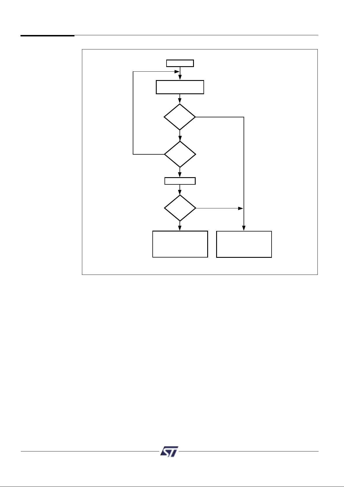
9.1.1.7.1 Data Polling
Polling on DQ7 is a method of checking whether a Program or Erase instruction is in
progress or has completed. Figure 4 shows the Data Polling algorithm.
When the MCU issues a programming instruction, the embedded algorithm within the
PSD935G2 begins. The MCU then reads the location of the word to be programmed in
Flash to check status. Data bit DQ7 of this location becomes the compliment of data
bit 7of the original data word to be programmed. The MCU continues to poll this location,
comparing DQ7 and monitoring the Error bit on DQ5. When the DQ7 matches data bit 7 of
the original data, and the Error bit at DQ5 remains ‘0’, then the embedded algorithm is
complete. If the Error bit at DQ5 is ‘1’, the MCU should test DQ7 again since DQ7 may
have changed simultaneously with DQ5 (see Figure 4).
The Error bit at DQ5 will be set if either an internal timeout occurred while the embedded
algorithm attempted to program the location or if the MCU attempted to program a ‘1’ to a
bit that was not erased (not erased is logic ‘0’).
It is suggested (as with all Flash memories) to read the location again after the embedded
programming algorithm has completed to compare the word that was written to Flash with
the word that was intended to be written.
When using the Data Polling method after an erase instruction, Figure 4 still applies.
However, DQ7 will be ‘0’ until the erase operation is complete. A ‘1’ on DQ5 will indicate
a timeout failure of the erase operation, a ‘0’ indicates no error. The MCU can read any
location within the sector being erased to get DQ7 and DQ5.
PSDsoft generates ANSI C code functions which implement these Data Polling
algorithms.
The
PSD935G2
Functional
Blocks
(cont.)
PSD9XX Family PSD935G2
22
Figure 4. Data Polling Flow Chart
START
READ DQ5 & DQ7
at VALID ADDRESS
YES
YES
YES
NO
NO
NO
DQ7
=
DATA7
DQ5
=1
DQ7
=
DATA
READ DQ7
FAIL
Program/Erase
Operation Failed
Issue Reset Instruction
PASS
Program/Erase
Operation is
Completed
The
PSD935G2
Functional
Blocks
(cont.)
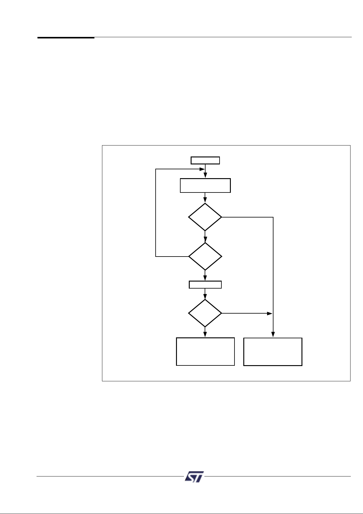
9.1.1.7.2 Data Toggle
Checking the Data Toggle bit on DQ6 is a method of determining whether a Program or
Erase instruction is in progress or has completed. Figure 5 shows the Data Toggle
algorithm.
When the MCU issues a programming instruction, the embedded algorithm within the
PSD935G2 begins. The MCU then reads the location to be programmed in Flash to check
status. Data bit DQ6 of this location will toggle each time the MCU reads this location until
the embedded algorithm is complete. The MCU continues to read this location, checking
DQ6 and monitoring the Error bit on DQ5. When DQ6 stops toggling (two consecutive
reads yield the same value), and the Error bit on DQ5 remains ‘0’, then the embedded
algorithm is complete. If the Error bit on DQ5 is ‘1’, the MCU should test DQ6 again, since
DQ6 may have changed simultaneously with DQ5 (see Figure 5).
The Error bit at DQ5 will be set if either an internal timeout occurred while the embedded
algorithm attempted to program, or if the MCU attempted to program a ‘1’ to a bit that was
not erased (not erased is logic ‘0’).
PSD935G2 PSD9XX Family
23
9.1.1.7.2 Data Toggle (cont.)
It is suggested (as with all Flash memories) to read the location again after the embedded
programming algorithm has completed to compare the word that was written to Flash with
the word that was intended to be written.
When using the Data Toggle method after an erase instructin, Figure 5 still applies. DQ6
will toggle until the erase operation is complete. A ‘1’ on DQ5 will indicate a timeout failure
of the erase operation, a ‘0’ indicates no error. The MCU can read any even location within
the sector being erased to get DQ6 and DQ5.
PSDsoft generates ANSI C code functions which implement these Data Toggling
algorithms.
The
PSD935G2
Functional
Blocks
(cont.)
Figure 5. Data Toggle Flow Chart
START
READ
DQ5 & DQ6
NO
YES
NO
YES
YES
NO
DQ6
=
TOGGLE
DQ5
=1
DQ6
=
TOGGLE
READ DQ6
FAIL
Program/Erase
Operation Failed
Issue Reset Instruction
PASS
Program/Erase
Operation is
Completed

PSD9XX Family PSD935G2
24
The
PSD935G2
Functional
Blocks
(cont.)
9.1.1.8 Unlock Bypass Instruction
The unlock bypass feature allows the system to program words to the flash memories
faster than using the standard program instruction. The unlock bypass instruction is
initiated by first writing two unlock cycles. This is followed by a third write cycle containing
the unlock bypass command, 20h (see Table 8). The flash memory then enters the unlock
bypass mode. A two-cycle Unlock Bypass Program instruction is all that is required to
program in this mode. The first cycle in this instruction contains the unlock bypass
programm command, A0h; the second cycle contains the program address and data.
Additional data is programmed in the same manner. This mode dispenses with the initial
two unlock cycles required in the standard program instruction, resulting in faster total
programming time. During the unlock bypass mode, only the Unlock Bypass Program and
Unlock Bypass Reset instructions are valid. To exit the unlock bypass mode, the system
must issue the two-cycle unlock bypass reset instruction. The first cycle must contain the
data 90h; the second cycle the data 00h. Addresses are don’t care for both cycles. The
Flash memory then returns to reading array data mode.
9.1.1.9 Erasing Flash Memory
9.1.1.9.1. Flash Bulk Erase Instruction
The Flash Bulk Erase instruction uses six write operations followed by a Read operation of
the status register, as described in Table 8. If any byte of the Bulk Erase instruction is
wrong, the Bulk Erase instruction aborts and the device is reset to the Read Flash memory
status.
During a Bulk Erase, the memory status may be checked by reading status bits DQ5, DQ6,
and DQ7, as detailed in section 9.1.1.7. The Error bit (DQ5) returns a ‘1’ if there has been
an Erase Failure (maximum number of erase cycles have been executed).
It is not necessary to program the array with 00h because the PSD935G2 will automatically
do this before erasing to 0FFh.
During execution of the Bulk Erase instruction, the Flash memory will not accept any
instructions.
9.1.1.9.2 Flash Sector Erase Instruction
The Sector Erase instruction uses six write operations, as described in Table 8. Additional
Flash Sector Erase confirm commands and Flash sector addresses can be written
subsequently to erase other Flash sectors in parallel, without further coded cycles, if the
additional instruction is transmitted in a shorter time than the timeout period of about
100 µs. The input of a new Sector Erase instruction will restart the time-out period.
The status of the internal timer can be monitored through the level of DQ3 (Erase time-out
bit). If DQ3 is ‘0’, the Sector Erase instruction has been received and the timeout is
counting. If DQ3 is ‘1’, the timeout has expired and the PSD935G2 is busy erasing the
Flash sector(s). Before and during Erase timeout, any instruction other than Erase suspend
and Erase Resume will abort the instruction and reset the device to Read Array mode.
It is not necessary to program the Flash sector with 00h as the PSD935G2 will do this
automatically before erasing.
During a Sector Erase, the memory status may be checked by reading status bits DQ5,
DQ6, and DQ7, as detailed in section 9.1.1.7.
During execution of the erase instruction, the Flash block logic accepts only Reset and
Erase Suspend instructions. Erasure of one Flash sector may be suspended, in order to
read data from another Flash sector, and then resumed.

PSD935G2 PSD9XX Family
25
The
PSD935G2
Functional
Blocks
(cont.)
9.1.1.9.3 Flash Erase Suspend Instruction
When a Flash Sector Erase operation is in progress, the Erase Suspend instruction will
suspend the operation by writing 0B0h to any even address when an appropriate Chip
Select (FSi or CSBOOTi) is true. (See Table 8). This allows reading of data from another
Flash sector after the Erase operation has been suspended. Erase suspend is accepted
only during the Flash Sector Erase instruction execution and defaults to read array
mode. An Erase Suspend instruction executed during an Erase timeout will, in addition to
suspending the erase, terminate the time out.
The Toggle Bit DQ6 stops toggling when the PSD935G2 internal logic is suspended. The
toggle Bit status must be monitored at an address within the Flash sector being erased.
The Toggle Bit will stop toggling between 0.1 µs and 15 µs after the Erase Suspend
instruction has been executed. The PSD935G2 will then automatically be set to Read
Flash Block Memory Array mode.
If an Erase Suspend instruction was executed, the following rules apply:
• Attempting to read from a Flash sector that was being erased will output invalid data.
• Reading from a Flash sector that was not being erased is valid.
• The Flash memory cannot be programmed, and will only respond to Erase Resume
and Reset instructions (read is an operation and is OK).
• If a Reset instruction is received, data in the Flash sector that was being erased will
be invalid.
9.1.1.9.4 Flash Erase Resume Instruction
If an Erase Suspend instruction was previously executed, the erase operation may be
resumed by this instruction. The Erase Resume instruction consists of writing 030h to any
even address while an appropriate Chip Select (FSi or CSBOOTi) is true. (See Table 8.)
9.1.1.10 Specific Features
9.1.1.10.1 Main Flash and Secondary Flash Sector Protect
Each sector of main Flash and secondary Flash memory can be separately protected
against Program and Erase functions. Sector Protection provides additional data
security because it disables all program or erase operations. This mode can be activated
(or deactivated) through the JTAG-ISP Port or a Device Programmer.
Sector protection can be selected for each sector using the PSDsoft program. This will
automatically protect selected sectors when the device is programmed through the JTAG
Port or a Device Programmer. Flash sectors can be unprotected to allow updating of their
contents using the JTAG Port or a Device Programmer. The microcontroller can read (but
cannot change) the sector protection bits.
Any attempt to program or erase a protected Flash sector will be ignored by the device.
The Verify operation will result in a read of the protected data. This allows a guarantee of
the retention of the Protection status.
The sector protection status can either be read by the MCU through the Flash protection
and secondary Flash protection registers (CSIOP) or use the read sector protection
instruction (Table 8).

PSD9XX Family PSD935G2
26
The
PSD935G2
Functional
Blocks
(cont.)
Bit 7 Bit 6 Bit 5 Bit 4 Bit 3 Bit 2 Bit 1 Bit 0
Sec7_Prot Sec6_Prot Sec5_Prot Sec4_Prot Sec3_Prot Sec2_Prot Sec1_Prot Sec0_Prot
Flash Protection Register
9.1.1.10.2 Reset Instruction
The Reset instruction consists of one write cycle (see Table 8). It can also be optionally
preceded by the standard two write decoding cycles (writing AAh to AAAh and 55h to
554h).
The Reset instruction must be executed after:
1. Reading the Flash Protection status or Flash ID using the Flash instruction.
2. When an error condition occurs (DQ5 goes high) during a Flash programming or erase
cycle.
The Reset instruction will reset the Flash to normal Read Mode immediately. However, if
there is an error condition (DQ5 goes high), the Flash memory will return to the Read
Mode in 25 µSeconds after the Reset instruction is issued.
The Reset instruction is ignored when it is issued during a Flash programming or Bulk
Erase cycle. The Reset instruction will abort the on going sector erase cycle and return the
Flash memory to normal Read Mode in 25 µSeconds.
9.1.1.10.3 Reset Pin Input
The reset pulse input from the pin will abort any operation in progress and reset the Flash
memory to Read Mode. When the reset occurs during a programming or erase cycle, the
Flash memory will take up to 25 µSeconds to return to Read Mode. It is recommended that
the reset pulse (except power on reset, see Reset Section) be at least 25 µSeconds such
that the Flash memory will always be ready for the MCU to fetch the boot code after reset
is over.
Bit Definitions:
Sec<i>_Prot 1 = Main Flash Sector <i> is write protected.
Sec<i>_Prot 0 = Main Flash Sector <i> is not write protected.
Bit 7 Bit 6 Bit 5 Bit 4 Bit 3 Bit 2 Bit 1 Bit 0
Security_
***
Sec3_Prot Sec2_Prot Sec1_Prot Sec0_Prot
Bit
Flash Boot Protection Register
Bit Definitions:
Sec<i>_Prot 1 = Flash Boot Sector <i> is write protected.
Sec<i>_Prot 0 = Flash Boot Sector <i> is not write protected.
Security_Bit 0 = Security Bit in device has not been set.
1 = Security Bit in device has been set.
Table 10. Sector Protection/Security Bit Definition
*: Not used.

PSD935G2 PSD9XX Family
27
The
PSD935G2
Functional
Blocks
(cont.)
9.1.2 SRAM
The SRAM is enabled when RS0 —the SRAM chip select output from the DPLD —is high.
RS0 can contain up to three product terms, allowing flexible memory mapping.
The SRAM can be backed up using an external battery. The external battery should be
connected to the Vstby pin (PE6). If you have an external battery connected to the
PSD935G2, the contents of the SRAM will be retained in the event of a power loss. The
contents of the SRAM will be retained so long as the battery voltage remains at 2V or
greater. If the supply voltage falls below the battery voltage, an internal power switchover
to the battery occurs.
Pin PE7 can be configured as an output that indicates when power is being drawn from the
external battery. This Vbaton signal will be high with the supply voltage falls below the battery voltage and the battery on PE6 is supplying power to the internal SRAM.
The chip select signal (RS0) for the SRAM, Vstby, and Vbaton are all configured using
PSDsoft.
9.1.3 Memory Select Signals
The main Flash (FSi), secondary Flash (CSBOOTi), and SRAM (RS0) memory select
signals are all outputs of the DPLD. They are defined using PSDsoft. The following rules
apply to the equations for the internal chip select signals:
1. Main Flash memory and secondary Flash memory sector select signals must not be
larger than the physical sector size.
2. Any main Flash memory sector must not be mapped in the same memory space as
another Main Flash sector.
3. A secondary Flash memory sector must not be mapped in the same memory space as
another Flash Boot sector.
4. SRAM and I/O spaces must not overlap.
5. A secondary Flash memory sector may overlap a main Flash memory sector. In case of
overlap, priority will be given to the Flash Boot sector.
6. SRAM and I/O spaces may overlap any other memory sector. Priority will be given to
the SRAM and I/O.
Example
FS0 is valid when the address is in the range of 8000h to BFFFh, CSBOOT0 is valid from
8000h to 9FFFh, and RS0 is valid from 8000h to 87FFh. Any address in the range of RS0
will always access the SRAM. Any address in the range of CSBOOT0 greater than 87FFh
(and less than 9FFFh) will automatically address Boot memory segment 0. Any address
greater than 9FFFh will access the Flash memory segment 0. You can see that half of the
Flash memory segment 0 and one-fourth of Boot segment 0 can not be accessed in this
example. Also note that an equation that defined FS1 to anywhere in the range of 8000h to
BFFFh would not be valid.
Figure 6 shows the priority levels for all memory components. Any component on a higher
level can overlap and has priority over any component on a lower level. Components on
the same level must not overlap. Level one has the highest priority and level 3 has the
lowest.
 Loading...